Note: Descriptions are shown in the official language in which they were submitted.
CA 03234840 2024-04-08
WO 2023/064034 PCT/US2022/040975
EMF SHIELD
CROSS-REFERENCE TO RELATED APPLICATIONS
[0001] This application claims benefit of priority with U.S. Provisional
Application Serial
No. 63/256,350, filed October 15, 2021; this application further claims
benefit of priority with
U.S. Provisional Application Serial No. 63/256,559 filed October 16, 2021; the
entire contents of
each are hereby incorporated by reference.
TECHNICAL FIELD
[0002] This invention relates to EMF shields; more particularly, ElVIF
shields configured
to scatter, disperse, and reflect an EMF signal.
BACKGROUND ART
[0003] The World Health Organization has classified radiofrequency
electromagnetic field
(E1VIF) signals as possibly carcinogenic to humans (Group 2B). Negative health
effects due to ElVIF
signals are only increased when devices such as wireless earbuds, virtual
reality headsets, and
wearable computer glasses are held in close proximity to a user's head for a
prolonged period of
time while constantly emitting EMF signals.
SUMMARY OF INVENTION
Technical Problem
[0004] Conventional ElVIF shields exist which either reflects or absorbs
the ElVIF signal.
However, shields which purely reflect the ElVIF signal usually redirect the
signal back to the user,
or alternatively to others nearby. Many reflective shields that are
commercially available provide
little to no SAR reduction to the user.
[0005] ElVIF shields which are designed to absorb and trap the ElVIF
signal are less
desirable due to the shield containing the ElVIF signal in close proximity to
the user's head for an
extended period of time. Maintaining the absorbed ElVIF signal when in close
proximity to the
user's head can also cause significant negative health effects. Furthermore,
energy absorbed by
-1-
CA 03234840 2024-04-08
WO 2023/064034 PCT/US2022/040975
an ElVIF shield increases in temperature and can cause irritation to the user
wearing the ElVIF shield
in close proximity to the user's skin.
Solution to Problem
[0006] An EMF shield is disclosed. The ElVIF shield comprises a
scattering layer and a
reflective layer having an exterior surface and an interior surface opposite
the exterior surface. The
scattering layer includes a metal coating disposed at the exterior surface.
The reflective layer
includes a first side and a second side opposite the first side, the first
side of the reflective layer
being coupled to the interior surface of the scattering layer, wherein the
reflective layer comprises
a dielectric material. The metal coating includes an adhesive coating for
coupling to an electronic
device.
[0007] The EMF shield is configured to scatter and reflect the ElVIF
signal as opposed to
purely reflecting or absorbing the signal. Based on position of the scattering
layer and the reflective
layer, the EMF signal will initially contact the scattering layer prior to
contacting the reflective
layer. The metal coating initially causes the ElVIF signal to disperse and
scatter. The scattered ElVIF
signal has a lower energy density and therefore becomes less harmful as
compared to the initial,
more concentrated signal. After the ElVIF signal is initially scattered by the
metal coating, the
reflective layer causes the ElVIF signal to reflect.
Advantageous Effects of Invention
[0008] By reflecting the already scattered signal, the ElVIF signal is
more easily broken up.
Harmful signals are not sent back to the user or others as is done by
conventional reflection shields.
[0009] Further, harmful signals are not absorbed and retained in near
proximity to users as
is done by conventional absorption shields. This can be especially dangerous
with newer
electronics which are designed to be in constant close proximity to a user's
head or face such as
VR headsets, wireless earbuds, wearable computer glasses, and the like.
[0010] The EMF shield comprises little to no absorption and therefore
does not increase in
temperature and irritate the user's skin.
BRIEF DESCRIPTION OF THE DRAWINGS
[0011] Other features, combinations, and embodiments will be appreciated
by one having
the ordinary level of skill in the art of antennas and accessories upon a
thorough review of the
following details and descriptions, particularly when reviewed in conjunction
with the drawings,
-2-
CA 03234840 2024-04-08
WO 2023/064034 PCT/US2022/040975
wherein:
[0012] FIG.1 shows a perspective view of an ElVIF shield in accordance
with a first
illustrated embodiment;
[0013] FIG.2 shows a side view of the ElVIF shield according to the first
illustrated
embodiment;
[0014] FIG.3 shows a perspective view of the ElVIF shield in accordance
with a second
illustrated embodiment;
[0015] FIG.4 shows a side view of the ElVIF shield according to the
second illustrated
embodiment;
[0016] FIG.5A-5D show various holographic patterns;
[0017] FIG.6 shows an ElVIF-reduced system comprising an ElVIF shield and
a wireless
earbud in accordance with a third illustrated embodiment;
[0018] FIG.7 shows an ElVIF-reduced system comprising an ElVIF shield and
wearable
computer glasses in accordance with a fourth illustrated embodiment; and
[0019] FIG.8 shows an ElVIF-reduced system comprising an ElVIF shield and
a virtual
reality (VR) headset in accordance with a fifth illustrated embodiment.
DETAILED DESCRIPTION
[0020] For purposes of explanation and not limitation, details and
descriptions of certain
preferred embodiments are hereinafter provided such that one having ordinary
skill in the art may
be enabled to make and use the invention. These details and descriptions are
representative only
of certain preferred embodiments, however, a myriad of other embodiments which
will not be
expressly described will be readily understood by one having skill in the art
upon a thorough
review of the instant disclosure. Accordingly, any reviewer of the instant
disclosure should
interpret the scope of the invention only by the claims, as such scope is not
intended to be limited
by the embodiments described and illustrated herein.
[0021] For purposes herein, the term "opaque" means a material which
allows no light to
pass through.
[0022] The term "EMF-absorbing material" means materials known to absorb
an ElVIF
signal including silver-nickel, carbon-steel, zinc, graphite, or other
materials known to one having
skill in the art to absorb ElVIF signals.
-3-
CA 03234840 2024-04-08
WO 2023/064034 PCT/US2022/040975
[0023] Unless explicitly defined herein, terms are to be construed in
accordance with the
plain and ordinary meaning as would be appreciated by one having skill in the
art.
General Description of Embodiments
[0024] In one embodiment, an EMF shield is disclosed. The ElVif shield
comprises a
scattering layer having an exterior surface and an interior surface opposite
the exterior surface, the
scattering layer comprising a metal coating disposed at the exterior surface,
a reflective layer
having a first side and a second side opposite the first side, the first side
of the reflective layer
coupled to the interior surface of the scattering layer, wherein the
reflective layer comprises a
dielectric material, and an adhesive coating coupled to the metal coating.
[0025] In some embodiments, the scattering layer may further comprise a
dielectric
substrate disposed between the metal coating and the reflective layer. The
dielectric substrate may
comprise a thermoplastic polymer. The thermoplastic polymer may comprise
polyester.
[0026] In some embodiments, the scattering layer may be opaque.
[0027] In some embodiments, the scattering may comprise metallized
polyethylene
terephthalate (PET).
[0028] In some embodiments, the metal coating may comprise aluminum.
[0029] In some embodiments, the metal coating may comprise a holographic
pattern. The
holographic pattern may comprise a prism-style holographic pattern.
[0030] In some embodiments, the dielectric material may comprise a
thermoplastic
polymer. The thermoplastic polymer may comprise polyester. The thermoplastic
polymer may
comprise polyethylene terephthalate.
[0031] In some embodiments, the reflective layer may be opaque.
[0032] In some embodiments, the ElVif shield may further comprise a
protective layer
coupled to the second side of the reflective layer. The protective layer may
comprise a
thermoplastic polymer. The thermoplastic polymer may comprise biaxially-
oriented
polypropylene
[0033] In some embodiments, the scattering layer and the reflective layer
may each be
devoid of ElVif -absorbing material.
[0034] In a second embodiment, an ElVif -reduced system is disclosed. The
ElVif -reduced
system comprises a wireless earbud and an ElVif shield. The wireless earbud
comprises an earbud
-4-
CA 03234840 2024-04-08
WO 2023/064034 PCT/US2022/040975
portion coupled to a stem portion, the stem portion having a stem-inner
surface and a stem-outer
surface opposite the stem-inner surface. The ElVif shield is coupled to the
stem-inner surface. The
EMF shield comprises a scattering layer having an exterior surface and an
interior surface opposite
the exterior surface, the scattering layer comprising a metal coating disposed
at the exterior surface,
a reflective layer having a first side and a second side opposite the first
side, the first side of the
reflective layer coupled to the interior surface of the scattering layer,
wherein the reflective layer
comprises a dielectric material, and an adhesive coating coupled to the metal
coating.
[0035] In some embodiments, at least a portion of the stem-outer surface
may be uncovered
by the EMF shield.
[0036] In a third embodiment, an ElVif -reduced system is disclosed. The
ElVif -reduced
system comprises a wearing computer glasses and an ElVif shield. The wearable
computer glasses
comprise lens disposed within a rim, a first temple coupled to the rim at a
first end piece, the first
temple including a first temple tip, and a second temple coupled to the rim at
a second end piece,
the second temple including a second temple tip. The ElVif shield is coupled
to an inner surface of
the first temple, the ElVif shield comprises a scattering layer having an
exterior surface and an
interior surface opposite the exterior surface, the scattering layer
comprising a metal coating
disposed at the exterior surface, a reflective layer having a first side and a
second side opposite the
first side, the first side of the reflective layer coupled to the interior
surface of the scattering layer,
wherein the reflective layer comprises a dielectric material, and an adhesive
coating coupled to the
metal coating.
[0037] In some embodiments, the ElVif shield may be disposed between the
first end piece
and the first temple tip.
[0038] In some embodiments, the ElVif -reduced system may further
comprise a secondary
EMF shield coupled to an inner surface of the second temple.
[0039] In a fourth embodiment, an ElVif -reduced system is disclosed. The
ElVif -reduced
system comprises a virtual reality headset and an ElVif shield. The virtual
reality headset
comprises a housing with a facial-interfacing surface, the facial interfacing
surface including a first
lens, a second lens, a forehead portion disposed above the first and second
lens, a first temple
portion disposed to a side of the first lens, a second temple portion disposed
to the side of the
second lens, and a nose portion disposed between the first and second lens.
The ElVif shield is
coupled to the forehead portion. The ElVif shield comprises a scattering layer
having an exterior
-5-
CA 03234840 2024-04-08
WO 2023/064034 PCT/US2022/040975
surface and an interior surface opposite the exterior surface, the scattering
layer comprising a metal
coating disposed at the exterior surface, a reflective layer having a first
side and a second side
opposite the first side, the first side of the reflective layer coupled to the
interior surface of the
scattering layer, wherein the reflective layer comprises a dielectric
material, and an adhesive
coating coupled to the metal coating.
[0040] In some embodiments, the ElVif shield may extend beyond each of
the first lens
and the second lens.
[0041] In some embodiments, the ElVif shield may comprise a plurality of
shield portions.
Manufacturing
[0042] The scattering layer may comprise metallized polyethylene
terephthalate (PET)
wherein the metallized PET comprises a dielectric substrate being PET and a
metal coating
disposed on one side of the PET substrate, such as aluminum. Thickness of the
PET substrate may
be 0.04mm. Other thicknesses may also be utilized. Thickness of the metal
coating is relatively
thin and may be between and inclusive of 5-30nm.
[0043] The reflective layer may comprise a thermoplastic polymer having
excellent
electro-insulating properties along with good mechanical strength and thermal
resistance. One
example may include PET. Thickness of the reflective layer can vary and in one
example may be
between 0.04mm-0.08mm, depending on thickness of the scattering layer. Other
thicknesses may
also be utilized as can be appreciated by one having skill in the art.
[0044] The protective layer preferably comprises a material resistant to
tear, oil, and water.
The protective layer may be a thermoplastic polymer such as polypropylene or
PVC. In one
example, the protective layer may be biaxially-oriented polypropylene (BOPP).
Other materials
may also be utilized. Color of the protective can vary and may be the same to
the electronic device
the ElVif shield is coupled with.
[0045] Each of the components of the ElVif shield and related system
described herein may
be manufactured and/or assembled in accordance with the conventional knowledge
and level of a
person having skill in the art.
[0046] While various details, features, combinations are described in the
illustrated
embodiments, one having skill in the art will appreciate a myriad of possible
alternative
combinations and arrangements of the features disclosed herein. As such, the
descriptions are
intended to be enabling only, and non-limiting. Instead, the spirit and scope
of the invention is set
-6-
CA 03234840 2024-04-08
WO 2023/064034 PCT/US2022/040975
forth in the appended claims.
First Illustrated Embodiment
[0047] Now turning to the drawings, FIG.1 shows a perspective view of an
ElVIF shield
(100) in accordance with a first illustrated embodiment. The ElVIF shield
comprises a plurality of
layers, namely, a scattering layer (110), a reflective layer (120), and a
protective layer (130). The
scattering layer comprises an exterior surface (111) configured to couple with
an electronic device,
and an interior surface (112) opposite the exterior surface. The interior
surface of the scattering
layer is coupled to a first side (121) of the reflective layer. A second side
(122) opposite the first
side is coupled to the protective layer (130). An adhesive coating (140) is
disposed on the exterior
surface for proper coupling to said electronic device.
[0048] The scattering layer (110) comprises a metal coating (113)
disposed on the exterior
surface (111). The metal coating comprises a thin layer, for example between
and inclusive of 3-
50nm. In a preferable embodiment, aluminum is used as the metal coating. Other
metals may be
utilized. The metal coating may comprise a holographic pattern to aid in
scattering an EMF signal.
The reflective layer (120) comprises a dielectric material configured to
reflect the ElVIF signal. The
EMF shield (100) is configured to scatter and reflect the ElVIF signal as
opposed to purely reflecting
or absorbing the signal. Based on position of the scattering layer and the
reflective layer, the ElVIF
signal will initially contact the scattering layer prior to contacting the
reflective layer. The metal
coating initially causes the ElVIF signal to disperse and scatter. The
scattered ElVIF signal has a
lower energy density and therefore becomes less harmful as compared to
initial, more concentrated
signal.
[0049] After the EMF signal is initially scattered by the metal coating
(113), the reflective
layer (120) causes the EMF signal to reflect. By reflecting the already
scattered signal, the EMF
signal is more easily broken up. Harmful signals are not sent back to the user
or others as is done
by conventional reflection shields. Further, harmful signals are not absorbed
and retained in near
proximity to users as is done by conventional absorption shields. This can be
especially dangerous
with newer electronics which are designed to be in constant close proximity to
a user's head or
face such as VR headsets, wireless earbuds, wearable computer glasses, and the
like.
[0050] The metal coating (113) is an important feature of the EMF shield
(100). If the
metal coating were not present to initially receive and scatter the EMF
signal, the EMF signal will
contact the dielectric material of the reflective layer (120) first, causing
the EMF signal to
-7-
CA 03234840 2024-04-08
WO 2023/064034 PCT/US2022/040975
undesirably return to the user. An initial scattering of the signal is an
important step to the ElVIF-
reduction process. The metal coating may comprise some or all of the
scattering layer.
[0051] In some embodiments, the scattering layer (110) and the reflective
layer (120) are
each devoid of any ElVIF-absorbing materials. In such embodiments devoid of
ElVIF-absorbing
material, there is no measurable increase in temperature during use. This
ensures all or virtually
all of the EMF signals are ultimately being reflected away from the user.
[0052] FIG.2 shows a side view of the ElVIF shield (100). according to
the first illustrated
embodiment. The ElVIF shield comprises a scattering layer (110), a protective
layer (130), and a
reflective layer (120) disposed therebetween. The scattering layer has an
exterior surface (111) and
an interior surface (112) opposite the exterior surface. The interior surface
is coupled to a first
side (121) of the reflective layer by an adhesive or other means of coupling
known to one having
skill in the art, such as a physical vapor deposition. Disposed on the
exterior surface is a metal
coating (113). Disposed on the metal coating is an adhesive coating (140) to
provide engagement
with an electronic device. As shown, all of the scattering layer is the metal
coating. In an alternative
embodiment, the metal coating comprises a portion of the scattering layer.
[0053] The reflective layer (120) comprises a dielectric material (123)
having insulative
properties to aid in reflection. Materials for the reflective layer may
include thermoplastic
polymers such as polyethylene terephthalate (PET). Other dielectric materials
may also be utilized
as can be appreciated by one having skill in the art. Thickness of the
reflective layer can vary.
Thicknesses between 0.04mm and 0.08mm have been shown to provide sufficient
reflective
properties to significantly reduce the ElVIF signal. In some embodiments,
sufficient thickness is
established by having the reflective layer be opaque. If the reflective layer
is not thick enough to
be opaque, then ElVIF-reduction is significantly reduced.
[0054] The protective layer (130) is coupled to a second side (122) of
the reflective layer
(120) to provide protective properties to the reflective layer and overall
ElVIF shield (100) such as
tear resistance, oil resistance, and water resistance.
Second Illustrated Embodiment
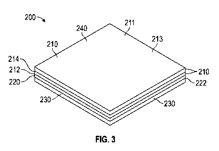
[0055] FIG.3 shows a perspective view of the ElVIF shield (200) in
accordance with a
second illustrated embodiment. The ElVIF shield comprises a scattering layer
(210) coupled to a
reflective (220). The reflective layer is further coupled to a protective
layer (230). The scattering
layer comprises a dielectric substrate (214) and a metal coating (213) coupled
to the dielectric
-8-
CA 03234840 2024-04-08
WO 2023/064034 PCT/US2022/040975
substrate. The metal coating is disposed on an exterior surface (211) of the
scattering layer wherein
the exterior surface comprises an adhesive coating (240) for coupling to an
electronic device. The
dielectric substrate is disposed at an interior surface (212) and is coupled
to the reflective layer.
The reflective layer, along with the dielectric substrate of the scattering
layer aid in the reflection
process of the ElVIF shield. An adhesive or other means of engagement is
disposed between the
scattering layer and the reflective layer, as well as the reflective layer and
the protective layer.
[0056] The scattering layer (210) having the metal coating (213) disposed
on the dielectric
substrate (214) allows for the manufacturing process to utilize conventional
materials, such as
metallized PET. However, unlike conventional metallized PET which is
transparent, the scattering
layer disclosed herein is opaque to ensure proper ElVIF-reduction. Increase of
the dielectric
substrate thickness of the scattering layer can allow for a decreased
reduction in thickness of the
reflective layer (220). In some embodiments, both the scattering layer and the
reflective layer are
individually opaque.
[0057] FIG.4 shows a side view of the ElVIF shield (200) according to the
second illustrated
embodiment. The ElVIF shield comprises a reflective layer (220) having a first
side (221) and a
second side (222) opposite the first side. A scattering layer (210) is coupled
to the first side and a
protective layer (230) is coupled to the second side. The scattering layer has
a metal coating (213)
disposed on an exterior surface (211) thereof. The scattering layer further
comprises a dielectric
substrate (214) such that the dielectric substrate is disposed between the
metal coating and the
reflective layer. The dielectric substate is coupled to the reflective layer
via adhesive or some
other means of coupling as can be appreciated by one having skill in the art.
The reflective layer
comprises a dielectric material (223). In some embodiments, the dielectric
material and the
dielectric substrate are a same material. In other embodiments, the dielectric
material and the
dielectric substrate are different materials.
[0058] The EMF shield (200) is configured to couple to an electronic
device at the exterior
surface (211) of the scattering layer (210). The metal coating (213) being
disposed on the exterior
surface ensures an ElVIF signal will initially contact the metal coating prior
to contacting any
insulative materials known to reflect an ElVIF signal, such as the dielectric
substrate (214) or the
reflective surface (220). The metal coating comprises an adhesive coating
(240) to allow the ElVIF
shield to properly couple to said electronic device.
[0059] Position of the metal coating (213) is important for proper EMF-
reduction. If the
-9-
CA 03234840 2024-04-08
WO 2023/064034 PCT/US2022/040975
metal coating was disposed at the interior surface (212) of the scattering
layer, as opposed to the
correct exterior surface (211), the ElVIF signal would initially contact the
dielectric substrate of the
scattering layer before it reached the metal coating. The dielectric substrate
would reflect most or
all of the ElVIF signal before it could be scattered and dispersed by the
metal coating, thereby
negatively impacting EMF reduction. In one experiment, the EMF shield (200)
was correctly
placed on a backside of a tablet and a laptop with a SAR reduction of 61% and
50% respectively.
When the ElVIF shield was reversed such that the ElVIF signal initially
contacted the protective
layer (230) and the reflective layer (220), the measured SAR reduction was
only 9% and 8%,
respectively.
[0060] FIG.5A-5D show various holographic patterns. The metal coating
(213) may
comprise a holographic pattern to aid in dispersion and scattering of the
ElVIF signal. The various
holographic patterns include a first holographic pattern (300), a second
holographic pattern (310),
a third holographic pattern (320), and a fourth holographic pattern (340). The
second holographic
pattern is characterized as having a cross-linked pattern. The third
holographic pattern is
characterized as having a dotted pattern. The fourth holographic pattern is
characterized as having
a mosaic pattern. The first holographic pattern comprises a prism-style
holographic with an even
distribution of the metal coating for an even dispersion and scattering of the
EMF signal.
Preferably, the metal coating of the ElVIF shield comprises the first
holographic pattern to provide
an even scattering of the ElVIF signal similar to visible light being evenly
scattered and divided
into the visible light's individual colors.
Third Illustrated Embodiment
[0061] FIG.6 shows an ElVIF-reduced system comprising an EMF shield (400)
and a
wireless earbud (450) in accordance with a third illustrated embodiment. The
wireless earbud
comprises an earbud portion (451) coupled to a stem portion (452). The stem
portion includes a
stem-inner surface (453) and a stem-outer surface (454) opposite the stem-
inner surface. When
the wireless earbud is worn by a user, the stem-inner surface is configured to
face the user's head
and may be configured to emit an ElVIF signal to a secondary wireless earbud
worn in the user's
other ear. The ElVIF shield is coupled to the wireless earbud at the stem-
inner surface. The ElVIF
shield comprises a scattering layer (410), a reflective layer (not shown), and
a protective layer
(430). The scattering layer comprises a metal coating (413) disposed on an
exterior surface (411)
thereof, wherein the metal coating comprises an adhesive coating (440) for
coupling to the wireless
-10-
CA 03234840 2024-04-08
WO 2023/064034 PCT/US2022/040975
earbud.
[0062] In some embodiments, at least a portion of the stem-outer surface
(454) is
uncovered by the ElVIF shield (400). If the ElVIF shield entirely surrounded
the stem portion (452)
including the stem-inner surface (453) and the stem-outer surface, some of the
ElVIF signal would
reflect back to the user's head.
Fourth Illustrated Embodiment
[0063] FIG.7 shows an ElVIF-reduced system comprising an EMF shield (500)
and
wearable computer glasses (550) in accordance with a fourth illustrated
embodiment. The wearable
computer glasses comprise a rim (551) with lens (552) coupled thereto along
with a bridge (553)
disposed between each of the lens. A first temple (554) is hingedly coupled to
the rim at a first
end piece (555). The first temple comprises a first inner side (556), a first
outer side (not shown),
and a first temple tip (557). A second temple (558) is hingedly coupled to the
rim at a second end
piece (559). The second temple comprises a second inner side (not shown), a
second outer side
(560), and a second temple tip (561). The ElVIF shield is coupled to the
wearable computer glasses
at the inner side of the first temple between the first temple tip and the
first end piece. Preferably,
the EMF shield is positioned at the first inner side prior to the where the
first temple begins to
taper due to the first temple tip.
[0064] In other embodiments, the ElVIF shield (500) is disposed at the
second inner side of
the second temple (558). In yet other embodiments, the ElVIF shield is coupled
to both the first
temple (554) and the second temple (558) at the first inner side (556) and the
second inner side,
respectively.
Fourth Illustrated Embodiment
[0065] FIG.8 shows an ElVIF-reduced system comprising an ElVIF shield
(600) and a virtual
reality (VR) headset (650) in accordance with a fifth illustrated embodiment.
The VR headset
comprises a housing (651) having a facial-interfacing surface (652). The
facial-interfacing surface
includes a first lens (657) and a second lens (658). Disposed above the first
and second lens is a
forehead portion (654) configured to contact a user's forehead. A nose portion
(653) is disposed
between the first and second lens wherein the nose portion is configured to
contact the user's nose.
A first temple portion (655) and a second temple portion (656) are positioned
on a side of the first
and second lens, respectively, and are each configured to position adjacent to
the user's temples
while earing the VR headset. A headband (659) is coupled to the housing. The
ElVIF shield is
-11-
CA 03234840 2024-04-08
WO 2023/064034 PCT/US2022/040975
coupled to the housing (651) at the forehead portion. In some embodiments, the
EMF shield
extends laterally beyond both the first lens and the second lens. The ElVif
shield may comprise a
single piece or may comprise a plurality of pieces to confirm to the curvature
of the facial-
interfacing surface.
-12-
CA 03234840 2024-04-08
WO 2023/064034
PCT/US2022/040975
Feature List
[0066] EMF shield (100; 200; 400; 500; 600)
[0067] scattering layer (110; 210; 410)
[0068] exterior surface (111; 211; 411)
[0069] interior surface (112; 212)
[0070] metal coating (113; 213; 413)
[0071] dielectric substrate (214)
[0072] reflective layer (120; 220)
[0073] first side (121; 221)
[0074] second side (122; 222)
[0075] dielectric material (123; 223)
[0076] protective layer (130; 230; 430; 530; 630)
[0077] adhesive coating (140; 240; 440)
[0078] first holographic pattern (300)
[0079] second holographic pattern (310)
[0080] third holographic pattern (320)
[0081] fourth holographic pattern (330)
[0082] wireless earbud (450)
[0083] earbud portion (451)
[0084] stem portion (452)
[0085] stem-inner surface (453)
[0086] stem-outer surface (454)
[0087] wearable computer glasses (550)
[0088] rim (551)
[0089] lens (552)
[0090] bridge (553)
[0091] first temple (554)
[0092] first end piece (555)
[0093] first inner side (556)
[0094] first temple tip (557)
[0095] second temple (558)
-13-
CA 03234840 2024-04-08
WO 2023/064034
PCT/US2022/040975
[0096] second end piece (559)
[0097] second outer side (560)
[0098] second temple tip (561)
[0099] virtual reality headset (650)
[0100] housing (651)
[0101] facial-interfacing surface (652)
[0102] nose portion (653)
[0103] forehead portion (654)
[0104] first temple portion (655)
[0105] second temple portion (656)
[0106] first lens (657)
[0107] second lens (658)
[0108] headband (659)
-14-