Note: Descriptions are shown in the official language in which they were submitted.
CA 03236738 2024-04-26
WO 2023/070215
PCT/CA2022/051592
INTEGRATED WIRELESS CHARGING BOOST RECTIFIER FOR
ELECTRIC VEHICLES
CROSS-REFERENCE
[0001] This application is a non-provisional of, and claims all priority
to, US Application No.
63/271,938, entitled "INTEGRATED WIRELESS CHARGING BOOST RECTIFIER FOR
ELECTRIC VEHICLES", filed 26-Oct-2021, incorporated herein by reference in its
entirety.
FIELD
[0002] Embodiments of the present disclosure generally relate to the
field of electric vehicle
charging, and more specifically, embodiments relate to devices, systems and
methods for
integrated wireless charging boost rectifier for electric vehicles.
INTRODUCTION
[0003] Wireless charging for electric vehicles is desirable as a
convenient alternative to
wired charging. In particular, a driver of an electric vehicle would be able
to park a vehicle
and couple to a charging pad disposed in a parking spot such that the vehicle
could then be
wirelessly charged.
[0004] However, specific electronic components may be required for
wireless charging so
that wireless charging can be effected, for example, at high frequencies, and
additional
electronic components add extra weight, volume, and cost, decreasing the
feasibility of electric
vehicles as an alternative to internal combustion engine vehicles as the
overall complexity and
range is increased.
[0005] Another deficiency of existing wireless charging mechanisms is that the
charging is
controlled only from the transmitter side, requiring a communication from the
vehicle to
indicate charge status.
[0006] This dependency can lead to additional requirements of the transmitter
and
additional complexity of the transmitter as the transmitter would then need
additional circuitry
to regulate power delivery. A transmitter manufacturer may also be able to
"lock in" electric
vehicles to specific proprietary standards, which may also be undesirable.
- 1 -
CA 03236738 2024-04-26
WO 2023/070215
PCT/CA2022/051592
SUMMARY
[0007] This application is directed to an approach for wireless /
contactless charging of
electric vehicles where, instead of using additional components or electrical
modules to
conduct the charging, the existing components (e.g., dual inverter drive) of
the vehicle are re-
purposed to support the wireless charging. While examples describe uses with a
dual inverter
drive, not all embodiments necessarily utilize a dual inverter drive.
[0008] In particular, the dual inverter drive (e.g., coupled with a
number of capacitors) can
be utilized as a high frequency (e.g., 85 kHz) rectifier for wireless
charging. A specific control
approach is also described that can be used to operate the dual-inverter as a
DC-DC converter
for regulating power delivery to the batteries. This approach is beneficial as
not only can there
be less electronic components, but power delivery control (e.g., duty-cycle
regulation) can
occur at the vehicle side (as opposed to other approaches only at the power
transmitter side).
[0009] In a first embodiment, an integrated on-board wireless charging
device for charging
an electric vehicle having a dual-inverter drivetrain during stand-still
operation of the electric
vehicle is proposed. The integrated on-board wireless charging device includes
a controller
circuit configured to control operation of at least four switches, Si, S2, S3,
and S4, Si and S2
coupled to a first capacitor of a compensated wireless coil and stacked in
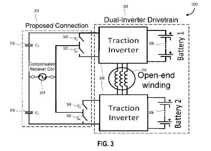
series to a first
traction stage of the dual inverter drive train having a first energy storage
and S3 and S4
coupled to a second capacitor of the compensated wireless coil and stacked in
series to a
second traction stage of the dual inverter drivetrain having a second energy
storage, Si and
S3, when operated, respectively cause a bypass of the first energy storage and
the second
energy storage, and S2 and S4, when operated, respectively connect the first
energy storage
and the second energy storage. The controller circuit controls operation of
the at least four
switches to selectively control interconnection between a wireless power
transmission system
delivering an input voltage Vdc and the first traction stage and the second
traction stage to
establish at least one of two modes of operation: a first active mode where
the first traction
stage and the second traction stage are used as a DC/DC converter to regulate
Vdc at a duty
cycle D when 0.5 < D < 1; a second active mode where the first traction stage
and the second
traction stage are used as a DC/DC converter to regulate Vdc at a duty cycle D
when 0 < D <
- 2 -
CA 03236738 2024-04-26
WO 2023/070215
PCT/CA2022/051592
0.5; wherein the at least four switches are utilized to establish conduction
paths through the
first traction stage and the second traction stage.
[0010] In some embodiments, a passive mode is provided for delivering
maximum charging
power where the first and second traction stage are not used as a DC/DC stage.
[0011] In some embodiments, the passive mode is utilized when regulation of
power
delivery by the integrated on-board wireless charging device is controlled by
transmitter-side
electronic devices operating in conjunction with a transmitter wireless coil,
and the at least two
modes of operation are utilized when regulation of the power delivery is to be
conducted on a
receiver side by controlling operation of the compensated wireless coil.
[0012] In some embodiments, during the passive mode, two conduction paths are
generated, a first conduction path during a positive half cycle, and a second
conduction path
during a negative half cycle, and the first conduction path includes
establishing a first set of
current loops by operating Si and S3 to bypass charging of the first energy
storage while
charging the second energy storage, and the second conduction path includes
establishing a
second set of current loops by operating S2 and S4 to charge the first energy
storage while
bypassing charging of the second energy storage.
[0013] In some embodiments, during the first active mode, two conduction
paths are
generated, a first conduction path during a positive half cycle by operating
S3 only that charges
the second energy storage while also increasing capacitor voltages with a DC
current, and a
second conduction path during a negative half cycle by operating S2 only that
charges the first
energy storage while also increasing capacitor voltages with the DC current;
and a conduction
path of the DC-DC stage serves to increase the capacitor voltages with the DC
current.
[0014] In some embodiments, during the second active mode, two conduction
paths are
generated, a first conduction path during a positive half cycle by operating
Si only that charges
the first capacitor while also increasing capacitor voltages with a DC
current, and a second
conduction path during a negative half cycle by operating S4 only that charges
the first energy
storage while also increasing capacitor voltages with the DC current; and
wherein a
- 3 -
CA 03236738 2024-04-26
WO 2023/070215
PCT/CA2022/051592
conduction path of the DC-DC stage serves to increase the capacitor voltages
with the DC
current.
[0015] In some embodiments, the controller circuit is adapted for
providing charge control
on receiver side power electronics.
[0016] In some embodiments, the controller circuit is adapted for providing
the charge
control through establishing three control loops adapted to regulate an
average current into
the first energy storage and the second energy storage.
[0017] In some embodiments, the device is configured for interoperation
with a conductive
charging system, the conductive charging system including four relays, R1, R2,
R3, and R4,
and two capacitors, Cl, and C2.
[0018] In some embodiments, the four relays are adapted to conduct
current in a receiver
coil and are free of requirements to switch under load.
[0019] In a variant embodiment, an integrated on-board wireless charging
device for
charging an electric vehicle having a dual-inverter drivetrain during stand-
still operation of the
electric vehicle is proposed. The integrated on-board wireless charging device
includes a
controller circuit configured to control operation of at least four switches,
Si, S2, S3, and S4,
Si and S2 coupled to a first capacitor of a compensated wireless coil and
stacked in series to
a first traction stage of the dual inverter drive train having a first energy
storage coupled to a
first capacitor C1 and a compensated wireless coil and S3 and S4 coupled to a
second energy
storage coupled to a second capacitor C2 and the compensated wireless coil, of
the
compensated wireless coil and stacked in series to a second traction stage of
the dual inverter
drivetrain having a second energy storage, Si and S3, when operated,
respectively cause a
bypass of the first energy storage and the second energy storage, and S2 and
S4, when
operated, respectively connect the first energy storage and the second energy
storage.
[0020] The controller circuit controls operation of the at least four
switches to selectively
control interconnection between of a wireless power transmission system
delivering an input
voltage Vdc to establish a passive mode of operation. In the passive mode, two
conduction
paths are generated, a first conduction path during a positive half cycle, and
a second
- 4 -
CA 03236738 2024-04-26
WO 2023/070215
PCT/CA2022/051592
conduction path during a negative half cycle, and the first conduction path
includes
establishing a first set of current loops by operating Si and S3 to bypass
charging of the first
energy storage while charging the second energy storage, and the second
conduction path
includes establishing a second set of current loops by operating S2 and S4 to
charge the first
energy storage while bypassing charging of the second energy storage.
[0021] In some embodiments, the integrated on-board wireless charging
device is
configured to operate in the passive mode when the device is delivering
maximum charging
power.
[0022] In some embodiments, the integrated on-board wireless charging
device is coupled
to a dual inverter drive train or an external power source, and the integrated
on-board wireless
charging device is configured to operate in an active mode in durations of
time when the
integrated on-board wireless charging device is not operating in the passive
mode.
[0023] In some embodiments, the integrated on-board wireless charging
device is
configured to operate in the passive mode when regulation of power delivery by
the integrated
on-board wireless charging device is controlled by transmitter-side electronic
devices
operating in conjunction with a transmitter wireless coil.
[0024] In some embodiments, the integrated on-board wireless charging
device is
configured to operate in an active mode in durations of time when the
integrated on-board
wireless charging device is not operating in the passive mode.
[0025] In some embodiments, during the active mode, two conduction paths are
generated,
a first conduction path during a positive half cycle by operating S3 only that
charges the second
energy storage while also increasing capacitor voltages with a DC current, and
a second
conduction path during a negative half cycle by operating S2 only that charges
the first energy
storage while also increasing capacitor voltages with the DC current; and
wherein a
conduction path of the DC-DC stage serves to increase the capacitor voltages
with the DC
current.
[0026] In some embodiments, during the active mode, two conduction paths are
generated,
a first conduction path during a positive half cycle by operating Si only that
charges the first
- 5 -
CA 03236738 2024-04-26
WO 2023/070215
PCT/CA2022/051592
capacitor while also increasing capacitor voltages with a DC current, and a
second conduction
path during a negative half cycle by operating S4 only that charges the first
energy storage
while also increasing capacitor voltages with the DC current; and wherein a
conduction path
of the DC-DC stage serves to increase the capacitor voltages with the DC
current.
[0027] In some embodiments, during the active mode, one of two active modes
are utilized:
a first active mode where the a first traction stage and the a second traction
stage are used
as a DC/DC converter to regulate Vdc at a duty cycle D when 0.5 < D < 1; and a
second active
mode where the first traction stage and the second traction stage are used as
a DC/DC
converter to regulate Vdc at a duty cycle D when 0 < D < 0.5.
[0028] In some embodiments, the integrated on-board wireless charging
device is
configured to operate in either the passive mode, the first active mode or the
second active
mode depending on a state of the duty cycle D, and the duty cycle D is
controllable.
[0029] In some embodiments, the integrated on-board wireless charging
device is
configured to operate in a passive mode and the voltage Vdc is regulated by a
converter.
[0030] In some embodiments, the duty cycle D is controllable.
[0031] Corresponding wireless charging methods and software / firmware program
products (e.g., non-transitory computer / machine readable media storing
machine
interpretable instruction sets for execution by a processor to carry out any
of the methods) are
contemplated.
DESCRIPTION OF THE FIGURES
[0032] In the figures, embodiments are illustrated by way of example. It
is to be expressly
understood that the description and figures are only for the purpose of
illustration and as an
aid to understanding.
[0033] Embodiments will now be described, by way of example only, with
reference to the
attached figures, wherein in the figures:
[0034] FIG. 1 is an example block schematic diagram of a wireless
charging solution.
- 6 -
CA 03236738 2024-04-26
WO 2023/070215
PCT/CA2022/051592
[0035] FIG. 2 is an example block schematic diagram of a system for a wireless
charging
solution.
[0036] FIG. 3 is a block schematic diagram of a system for a connection
of the wireless
receiver coil to an existing drivetrain, according to some embodiments.
[0037] FIG. 4 is a block schematic diagram of a system for an integrated
wireless charge
that leverages a dual-inverter drivetrain, according to some embodiments.
[0038] FIG. 5 is a block schematic diagram of a system for an integrated
wireless charger,
based on the integrated single phase charger, according to some embodiments.
[0039] FIG. 6 is an example block schematic diagram of a system for a wireless
power
transmission system, according to some embodiments. A wireless power
transmission system
is a non-limiting example of a conductive charging system.
[0040] FIG. 7A is an example block schematic diagram of a circuit during
passive operating
mode of the conductive path during positive half cycle (/õ > 0). As noted
herein, in some
embodiments, the dual inverter is not required for this operating mode. For
example, the
switches and the capacitors of the circuit can be used to charge dual energy
storage devices,
in another variant embodiment.
[0041] FIG. 7B is an example block schematic diagram of a circuit during
passive operating
mode of the conductive path during negative half cycle (/õ < 0). As noted
herein, in some
embodiments, the dual inverter is not required for this operating mode. For
example, the
switches and the capacitors of the circuit can be used to charge dual energy
storage devices,
in another variant embodiment.
[0042] FIG. 8A is an example block schematic diagram of a circuit during
active mode A
operation where 0.5 < D < 1, specifically of a conduction path during postive
half cycle (/õ >
0).
- 7 -
CA 03236738 2024-04-26
WO 2023/070215
PCT/CA2022/051592
[0043] FIG. 8B is an example block schematic diagram of a circuit during
active mode A
operation where 0.5 <D < 1, specifically of a conduction path during negative
half cycle (/õ <
0).
[0044] FIG. 9A is an example block schematic diagram of a circuit during
active mode B
operation where 0 < D < 0.5, specifically of a conduction path during positive
half cycle (/õ >
0).
[0045] FIG. 9B is an example block schematic diagram of a circuit during
active mode B
operation where 0 < D < 0.5, specifically of a conduction path during negative
half cycle (/õ <
0).
[0046] FIG. 10 is a plot of normalized charging power into the batteries
(Pchg) versus dc-dc
stage duty cycle (D).
[0047] FIG. 11 is an example block schematic diagram of a dc-dc stage
implemented using
the traction inverters and motor.
[0048] FIG. 12 is a plot of a normalized inductor current ripple as a
function of the duty cycle
(D).
[0049] FIG. 13A is a block schematic diagram of a control approach of an
integrated
charger, according to some embodiments.
[0050] FIG. 13B is a circuit diagram, according to some embodiments.
[0051] FIG. 14 is a schematic flowchart for the states of the wireless
transmitter and the
integrated charger.
[0052] FIG. 15 is an example of a simulation of a complete charging cycle,
where Vb*_õ9 =
360V and the coils are well-aligned.
[0053] FIG. 16 is an example of a simulation of complete charging cycle,
where irb _õ9 =
360V and the coils are misaligned.
- 8 -
CA 03236738 2024-04-26
WO 2023/070215
PCT/CA2022/051592
[0054] FIG. 17 is a depiction of the experimental setup showing the
system
[0055] FIG. 18 is a depiction of the dual inverter drive integrated
charger, along with the EV
machine.
[0056] FIG. 19 is a depiction of a system performance operating in
passive mode. The
inherent charge balancing is also shown by setting Vbi= 350V while Vb2=315V.
[0057] FIG. 20 is a depiction of a system performance operating in active mode
with D =
0.34.
[0058] FIG. 21 is a plot showing the experimentally measured charging
power into the
batteries ('N) versus the dc-dc duty cycle (D).
[0059] FIG. 22 is a depiction of a battery current step from 5A to 8A, with
the battery currents
offset.
[0060] FIG. 23 is a depiction of a set change in 6(0 from 0 to 0.1,
showing the ability of the
converter to set individual battery currents, at any speed, with no controller
interaction with the
CC/CV average controllers.
[0061] FIG. 24 is a plot of the overall system efficiency, measuring loss
('N) in three main
operating modes (aligned (passive), aligned (active, D = 0.5), and misaligned
(active, D =
0.337).
[0062] FIG. 25 is a block schematic of an example commercial implementation of
the
integrated charger, according to some embodiments.
[0063] FIG. 26 is a block schematic of another example commercial
implementation of the
integrated charger, according to some embodiments.
DETAILED DESCRIPTION
[0064] This application is directed to an approach for wireless /
contactless charging of
electric vehicles where, instead of using additional components or electrical
modules to
conduct the charging, the existing components (e.g., dual inverter drive) of
the vehicle are re-
- 9 -
CA 03236738 2024-04-26
WO 2023/070215
PCT/CA2022/051592
purposed to support the wireless charging. As noted herein, not all
embodiments necessarily
have a dual inverter drive. In a variant embodiment, the circuit topology can
be used such
that switches and the capacitors of the circuit can be used to charge dual
energy storage
devices. A number of different operating modes are proposed herein, including
a passive
.. mode and two active modes. The proposed circuit topology can include a
proposed wireless
connection that is a compensated wireless coil in conjunction with two
capacitors and four
switches, which can be coupled to a dual inverter drivetrain or a dual energy
storage devices
(e.g., dual batteries). In some embodiments, a system includes both the
proposed wireless
connection, and a dual inverter drivetrain or the dual energy storage devices.
[0065] The dual inverter drive (e.g., coupled with a number of capacitors)
can be utilized as
a high frequency (e.g., nominally at 85 kHz, but could vary, such as a range
from 80-90 kHz)
rectifier for wireless charging. Other frequencies are possible, for example,
as standards
change (e.g., 80-90 kHz may be selected due to other considerations such as
avoiding
interference with other types of signal propagation), and the proposed circuit
of various
embodiments can be adapted to different frequencies as well in view of device
requirements.
[0066] Being able to re-purpose existing components is useful to reduce
an overall weight,
volume, cost, and complexity of the electric vehicle while still providing
wireless / contactless
charging. While some embodiments are directed to wireless charging of electric
vehicles,
there may be non-electric vehicle operation for controlling power delivery to
other types of
circuits that have dual-inverter topologies, such as multi-port converters for
solar panels,
among others. In these variations, the motor of the electric vehicle could be
replaced with an
inductor.
[0067] A control approach is also described that can be used to regulate power
into storage
devices, such as batteries. For example, a specific control approach can be
used to operate
the dual-inverter as a DC-DC converter for regulating power into the
batteries. This approach
is beneficial as not only can there be less electronic components, but power
delivery control
(e.g., duty-cycle regulation) can occur at the vehicle side (as opposed to
other approaches at
the power transmitter side). In an embodiment, an approach is directed to the
reduced-
component rectifier described. In a variant embodiment, the approach is
directed to the
reduced component rectifier that is also controlled to provide power
regulation.
- 10-
CA 03236738 2024-04-26
WO 2023/070215
PCT/CA2022/051592
[0068] Integrated on-board charging has gained significant due to the
potential cost and
weight savings in the vehicle [1]-[5]. Integrated charging involves re-
purposing the existing
drivetrain components, namely the power electronics and motor, as part of the
charging
system. In doing so, this can eliminate additional power electronics and
magnetics (and their
associated cooling requirements, connectors, and enclosures) required for
charging from an
ac grid. Another advantage of integrated chargers are their high charging
power. As integrated
chargers use the high power traction power electronics and motor, they are
capable of
processing over 100 kW of power. Therefore, when used for charging, they allow
higher
charging currents, resulting in faster charging speeds.
[0069] Various integrated chargers have been proposed based on different
drivetrain
configurations. A solution proposed in [6] demonstrated ac charging from a
single phase grid
by connecting the grid through a diode bridge between the motor's neutral
point and the
negative dc terminal of the battery. In this case, the traction inverter was
operated as a three-
phase PFC boost converter.
[0070] Renault's commercially sold integrated charging solution involves
using a current
source converter front-end to interface the drivetrain to the grid [7], [8].
An topology based on
the dual-inverter drive architecture was introduced in [9], where a silicon
carbide (SiC) active
front end (AFE) was added to allow bidirectional ac charging at up to 19.2kW.
Peak efficiencies
of 97% were reported.
[0071] While conductive charging is the most common charging method today in
most EVs,
inductive/wireless charging has also been gaining popularity for its improved
convenience and
safety [10].
[0072] FIG. 1 is an example block schematic diagram of a wireless
charging solution.
System 100 includes a battery device coupled to a receiver power electronics
device is
coupled to some communication embodiments and some compensation network
embodiments. The receiver power electronics device is coupled, in some
embodiments, to a
transmitter power electronics device. The transmitter power electronics device
is coupled in
some embodiments to some communication embodiments and some compensation
network
embodiments.
-11 -
CA 03236738 2024-04-26
WO 2023/070215
PCT/CA2022/051592
[0073] While potentially not as efficient as conductive charging, some
applications benefit
greatly from wireless charging, such as transit vehicles, autonomous vehicles,
as well as
vehicles operating in harsh conditions [11]. Wireless charging can be more
convenient and
useful, especially in areas of limited real-estate, such as in city centers,
or in situations where
.. there is little time or labor available to connect devices for conductive
charging (e.g., where
turnaround time is short between scheduled vehicles). Transmissions efficiency
has improved
for wireless chargers, especially under mis-aligned cases [12]-[15]. In [15],
the losses
associated with transmitter-receiver coil misalignment were reduced by
employing field-
oriented control to direct the magnetic field toward the receiver.
[0074] However, wireless charging systems are usually very expensive and low
power
compared to even single-phase ac charging. That being said, advances have
enabled high
power wireless power transfer (20kW+) [16]. For example, in [17] a 50kW
wireless power
transfer was demonstrated. Aside from the wireless coils, wireless power
transfer also requires
power electronics. Requiring power electronics means that the higher the
power, the larger
and more expensive are the required power electronics on-board the vehicle.
[0075] In some instances, cost and weight savings on-board the car are made by
placing a
passive, rectifying converter on-board the car, and having the transmitter
power electronics
perform the necessary charge control. In this approach, the controller
feedback variables must
be transmitted form the vehicle using a form of wireless communication in real
time. This is a
technical deficiency and can pose a challenge for the robustness and security
of the
vehicle/charger [18].
[0076] In order to eliminate the need for wireless communication of
sensitive controller
feedback signals, [19]-[23] have implemented the control on the receiver (on-
board) side.
However, in all of these cases, the converters on-board the vehicle become
significantly more
complex and expensive, making it prohibitive to scale up the charging power.
[0077] The feasibility of an integrated wireless system is used in order to
simultaneously
address the high cost and low charging power of current wireless charging
solutions.
Specifically, re-purposing existing components on the vehicle used for the
drivetrain/charging
(eg, magnetics such as the motor), is proposed as a potential approach to
serve as part of the
- 12 -
CA 03236738 2024-04-26
WO 2023/070215
PCT/CA2022/051592
receiver-side power electronics in the car. This reduces the cost associated
with needing
discrete wireless charging power electronics, while enabling higher charging
power.
[0078] The approach in [24] re-purposed the vehicle's on-board single-phase
charger to
perform the majority of the receiver side charge control. This can be a large
cost savings,
however it still requires a traditional on-board single phase ac charger and
is limited to the
power of that charger (usually around 6.6kVV).
[0079] FIG. 2 is an example block schematic diagram of a system for a wireless
charging
solution.
[0080] In [25], better integration was achieved by connecting the
wireless receiver coil
through a diode bridge between the neutral point and the negative dc terminal
of the battery,
as shown in FIG. 2. System 200 builds on the integrated single phase charger
in [6].
[0081] However, this requires an additional diode bridge, and it still
requires traditional
transmitter side control. Furthermore, it requires that the drivetrain carry
high frequency
wireless charging currents, which will either substantially degrade
efficiency, or require costly
optimization of the drivetrain to limit high frequency losses.
[0082] This approach proposes an integrated wireless charger, as shown in FIG.
3.
[0083] FIG. 3 is a block schematic diagram of a system that can be used, for
example, for
a connection of the wireless receiver coil to an existing drivetrain detailed
in [9], according to
some embodiments. System 300 comprises several blocks; a dual inverter drive
302,
comprises of two traction inverters 304, two batteries (306 and 308), and an
open winding
machine 310, as well as the connection 312 to the compensated wireless
receiver coil 314 for
receiving power delivery from a corresponding transmitter coil. As noted
herein, while in FIG.
3 a dual inverter drivetrain is shown, it is important to note that in some
embodiments, the
proposed connection does not necessarily need to be connected to a dual
inverter or traction
.. inverters, but can be used instead to couple to different circuits, such as
a dual energy storage
device (e.g., dual batteries).
- 13-
CA 03236738 2024-04-26
WO 2023/070215
PCT/CA2022/051592
[0084] Compensation is added to the natural impedance of the coils themselves,
where at
high frequencies, the coil itself will behave as a high impedance device, and
the compensation
(e.g., by adding capacitors; a capacitor, an inductor, and a capacitor, a
capacitor and an
inductor) can cause cancellation of the impedance of the coil to increase an
ease of driving a
current through the coil. The proposed system could operate without
compensation of the
receiver coil, but the system would encounter high impedances. The proposed
connection
(e.g., circuit) requires at least 2 small capacitors (316 and 318) as well as
four switches (320,
322, 324, and 326). A detailed schematic is shown in FIG. 4.
[0085] FIG. 4 is a block schematic diagram of a system for an integrated
wireless charge
that leverages a dual-inverter drivetrain, according to some embodiments.
[0086] System 400 is comprised of a dual inverter drivetrain 402 coupled
to a wireless
connection 404. The dual inverter drivetrain 402 comprises of two inverters
(406 and 408), a
motor 410, as well as the connection 404 to the compensated wireless coil 412.
The proposed
wireless connection comprises of two capacitors (414 and 416), as well as four
switches (418,
420, 422, and 424).
[0087] Variations are possible and the components described are provided as a
non-
limiting, illustrative example. Switch 51, 418 and switch S2, 420, are stacked
in series where
the top of 51 and the bottom of S2 are connected across the battery, and the
midpoint between
51 and S2 is connected to the wireless coil.
[0088] When 51 or S2 are operated, a current loop is established that,
depending on the
operating mode, may direct current into capacitor Cl or battery Bl, depending
on the direction
of energy flow. 51 and S2 can be switched on intentionally by applying a
certain stimulus or
they can commutate naturally with the flow of current. The frequency of the
switching should
be at least equal to the fundamental frequency of the wireless receiver coil
current. 51 and S2
are operating so as to maintain a continuous flow of current from the wireless
coil, but can be
used to direct this flow of current into other components of the system, which
can result in a
different amount of power extracted from the wireless coil. 51 and S2 are
never switched on
together. An example of 51 switched on can be observed in FIG. 9A. An example
of S2
switched on can be observed in FIG. 8B.
- 14 -
CA 03236738 2024-04-26
WO 2023/070215
PCT/CA2022/051592
[0089] When S3 or S4 are operated, a current loop is established that,
depending on the
operating mode, may direct current into capacitor 02 or battery B2, depending
on the direction
of energy flow. S3 and S4 can be switched on intentionally by applying a
certain stimulus or
they can commutate naturally with the flow of current. The frequency of the
switching should
be at least equal to the fundamental frequency of the wireless receiver coil
current. S3 and S4
are operating so as to maintain a continuous flow of current from the wireless
coil, but can be
used to direct this flow of current into other components of the system, which
can result in a
different amount of power extracted from the wireless coil. S3 and S4 are
never switched on
together. An example of S3 switched on can be observed in FIG. 8A. An example
of S4
switched on can be observed in FIG. 9B.
[0090] The system 400 is shown as an example. Depending on a configuration
(e.g., Active
Mode B + Passive Mode Only), there may be less switches (e.g., only the
switches required
for a particular mode) required, and accordingly, the number of switches does
not necessarily
need to be four (e.g., switches shown that are never used for a particular
mode can simply not
.. be present). This occurs, for example, in example embodiments where the
circuit is to be
operated only active mode A, or only active mode B. If passive mode is to be
incorporated in
another embodiment (e.g., an ability to switch between passive mode and either
(or both) of
active modes A and B), then all four switches need to be present as all four
switches are used
in passive mode (see FIGS. 7A, 7B).
[0091] With respect to FIG. 4, the switches of the dual inverter drive
(labelled Sal, etc.)
can be operated in respect of a duty cycle D. The duty cycle D can be used to
control the
state of operation, for example, to swap between the passive mode of operation
and/or the
various active modes. In a first embodiment, the device is adapted to only
operate in the
passive mode. As noted above, the device operating in the passive mode does
not always
require the dual inverter drive or traction stages, and can instead, for
example, charge dual
batteries (e.g., the proposed wireless connection 404 can be coupled to other
types of circuits).
In a second embodiment, the device is adapted to operate in the passive mode
in addition to
the first active mode. In a third embodiment, the device is adapted to operate
in the passive
mode in addition to the second active mode. In a fourth embodiment, the device
is adapted
to operate in the passive mode in addition to both the first active mode and
the second active
- 15-
CA 03236738 2024-04-26
WO 2023/070215
PCT/CA2022/051592
mode depending on the value of D. In a fifth embodiment, the device is adapted
to operate in
the passive mode in addition to both the first active mode and the second
active mode and
the mode is controlled by a switch or controller circuit in respect of the
value of D.
[0092] This is effectively shown as a simplified representation in FIGS.
8A, 8B, 9A, 9B as
virtual voltage source having the voltage equal to the duty cycle multiplied
by the sum of the
battery voltages: D (Vb1 + Vb2). As noted in these figures, it provides an
additional current
loop, which can serve to control the voltage across the rectifying capacitors.
[0093] The proposed wireless connection 404 could be mounted onto the dual
inverter
drivetrain 402, and can be applied, for example, on a retrofit of an electric
vehicle to add
wireless charging capabilities (e.g., adding an additional connection stage),
or, in another
example, onto a build of an all new electric vehicle as an integrated part of
the drivetrain during
manufacturing.
[0094] One embodiment of FIG. 4 is to use the dual inverter drive with
integrated single
phase ac charging, as proposed in [9].
[0095] If a dual inverter drive with integrated single phase ac charging,
as proposed in [9]
is used, then the only additional components required will be two small
capacitors (and some
small relays for reconfiguration in order to maintain ac single phase ac
charging capability).
This detailed charger schematic is shown in FIG. 5.
[0096] FIG. 5 is a block schematic diagram of a system for an integrated
wireless charger,
based on the integrated single phase charger, according to some embodiments.
[0097] System 500 comprises an integrated AC charger 502 utilizing a dual
inverter
drivetrain 504 coupled to a wireless connection 506, in some embodiment. In
FIG. 5, the
switches S1-S4 are not only useful for wireless charging, but can be used for
other purposes,
such as AC charging, bringing additional flexibility of utilization (e.g.,
further justifying inclusion
of the switches). For AC charging, switches S1-S4 could be used as rectifier
to connect an
AC grid voltage to the dual inverter drive. For example, EVSE (electric
vehicle supply
equipment) would be a charging outlet for a connection for AC charging when
connected to
an AC grid.
- 16 -
CA 03236738 2024-04-26
WO 2023/070215
PCT/CA2022/051592
[0098] System 500 saves cost of the power electronic components themselves,
and also
on the secondary requirements (e.g., liquid cooling plates, controller board,
sensors,
protection, battery contactors, enclosures, connectors, etc.). The direct
connection to the
drivetrain allows for the charging of both isolated batteries in the dual
inverter drive from a
single receiver coil.
[0099] Current wireless charging technologies are not designed to charge
two isolated
batteries which would make them incompatible with dual-inverter drivetrains.
Furthermore, the
power electronics on the drivetrain can be leveraged to operate like a voltage
doubler. This
halves the voltage on the receiver coil, which in turn requires less flux from
the transmitter coil.
This improves wireless transmission efficiency as it results in a lower
current in the wireless
transmitter coil, which is often physically large with many turns, and
therefore subject to high
ohmic losses.
[00100] II. Proposed Topology
[00101] A challenge with using an integrated charger as the power electronics
for a wireless
system is the high frequency requirements of the wireless power transfer. The
standard for
wireless power transfer recommends a frequency of 85khz. Other frequencies are
possible.
[00102] From the drivetrain perspective, this high frequency current can
create significant
losses.
[00103] The large IGBT-based traction inverters cannot switch that fast due to
the large
device tail currents, and the motor magnetics may incur significant core loss.
The motor
windings will also incur significant resistive losses, due to the skin effect
phenomenon. As
such, the drivetrain operating frequency must be kept low, and within the
conventional
operating range.
[00104] The two grid stage half bridges introduced in [9] can be implemented
such that they
can handle higher frequency currents. It is advantageous to use SiC devices
for the grid stages
for ac charging, as it is the main contributor of switching loss and
determinate of the total
harmonic distortion (THD) of the system [9].
- 17-
CA 03236738 2024-04-26
WO 2023/070215
PCT/CA2022/051592
[00105] It would be desireable to leverage these fast switching devices to
rectify the high
frequency wireless currents.
[00106] In order to allow this system to perform either ac charging as
demonstrated in [9]
and wireless charging, relays R1-R4 must be closed during wireless charging,
and opened
during ac charging. In this case, the ac grid is only connected when the
Electric Vehicle Supple
Equipment (EVSE) is plugged into the vehicle and enabled (therefore no
additional contactors
are required on-board).
[00107] Relays R1-R4 and capacitors C1, C2 are the only additional components
required to
enable the integrated single-phase ac charger, to also serve as the power
electronics for the
.. wireless transmission system. As R1-R4 are only used for configuration of
the circuit; they do
not need to switch under load, and need only carry the current in the receiver
coil. R1-R4 are
distinct from switches S1-S4. For example, one could open all of R1-R4 for AC
charging, and
one could close all of R1-R4 for wireless charging (effectively acting as a
toggle between AC
and wireless charging).
[00108] Therefore, they are both small and inexpensive. If single phase ac
charging is not
desired, system 400 can be constructed, and the switches S1-S4 chosen
appropriately.
[00109] Cl and C2 are capacitors (e.g., a film capacitor but could be
implemented with other
capacitor technologies), and could be rated appropriately (e.g., as they only
carry a high
frequency component, they can have a small capacitance value). An example
capacitance
value could be 10 uF. Other values, as non-limiting examples, could be larger
values or
smaller values (but too small could impart unwanted noise).
[00110] A. Wireless Coil Topology
[00111] FIG. 6 is an example block schematic diagram of a system for a
wireless power
transmission system, according to some embodiments. It is important to note
that a wireless
power transmission system is a non-limiting example of a conductive charging
system, and
that embodiments are contemplated for operation with various types of
conductive charging
systems. A compensated wireless coil is shown, which can be used for insertion
into FIG. 7A,
FIG. 7B, FIG. 8A, FIG. 8B, FIG. 9A, FIG. 9B. Variations are possible.
- 18-
CA 03236738 2024-04-26
WO 2023/070215
PCT/CA2022/051592
[00112] In system 600, the coils are rectangular coils (602 and 604) which
have full series
compensation on the primary 602 and secondary 604 side. The transmitter coil
606 is excited
using a full bridge converter 608 that induces a voltage, over a gap 610, for
example, 200 mm
(other gaps are possible depending on a class of vehicle for example, as SUVs,
trucks may
have different ground clearances compared to sports cars), onto the receiver
coil 606. Finally,
the compensated receiver coil 612 is connected to the integrated wireless
charger 614. The
detailed parameters are described later in Table 2. The coils may have
geometries other than
rectangular coils as rectangular coils are used as a non-limiting example of a
sample topology.
Other geometries could be circular, 3D coils, among others.
[00113] In this embodiment, it is expected that the charge control of the
batteries is
performed by the receiver side power electronics. In the analysis below, it is
assumed that the
wireless receiver is compensated such that it behaves as a current source.
Details regarding
different compensation techniques can be found in [26].
[00114] The main relations / equations for the coils can be written as,
[VZi Z [ Itx]
[00115] o ¨ ZM Z2 lirrx (1)
[00116] Where (neglecting parasitic resistances),
1
= jcuLp ______________________________________________
jwCp (2)
Z2 = jalLs 1 RL
(3)
jwC,
[00117] Zm = jcuM
(4)
[00118] Resistance RL represents the equivalent load of the integrated
charger. Choosing
Cp and Cs. for full compensation yields,
0
(5)
[00119] Z2 0
(6)
- 19-
CA 03236738 2024-04-26
WO 2023/070215
PCT/CA2022/051592
[00120] Combining (1) with (5) and (6) yield approximated equations for the
currents in the
transmitter and receiver,
RLVtx
x
[00121] M
(7)
Vtx
1-rx
[00122] Zm
(8)
[00123] To maximize efficiency of the wireless transmission system, it is
desired to minimize
the transmitter current [27]. Considering (7), it appears that RL must be
reduced in order to
reduce the transmitter current, /tx. In this case, using the fundamental
frequency approach,
RL is,
8 v2
_____________________________________________ dc
72po 4
[00124] RL
(9)
[00125] Where P0 is the desired charging power into the batteries, and Vd, is
the rail-to-rail
voltage shown in FIG. 5.
[00126] Connecting the wireless receiver to the mid-point of capacitors C1, C2
yields a voltage
doubling effect, since the receiver only sees half of Vdc. This effectively
reduces the resistance
(RL) seen by the receiver coil by a factor of four, compared to a conventional
full-bridge
rectifier. This immediately means the transmitter current will be reduced by a
factor of four,
according to (7). In addition, Vdc can be reduced by operating traction
inverter as a dc-dc
converter. This is the main mechanism for controlling the power delivered to
the batteries,
from the wireless transfer system.
[00127] While the embodiment considers the use of this specific wireless
transmission
topology, it can be used with other systems. For example, if improved coil-to-
coil efficiency
under misalignment is desired, the described bipolar transmitter coil topology
described in [28]
is used. The only requirement from the wireless transmission system is that
the receiver must
be compensated to behave as a current source and must have only two terminals.
- 20 -
CA 03236738 2024-04-26
WO 2023/070215
PCT/CA2022/051592
[00128] B. Principle of Operation
[00129] The integrated charger will have three main modes of operation:
Passive mode,
Active mode A and Active mode B.
[00130] 1) Passive Mode: Passive mode is enabled by not utilizing the traction
inverters as
a dc/dc stage. This mode of operation is used when the charging controllers
request the
maximum possible charging power, or when charge control will be done solely
from the
transmitter side. This is an advantageous operating mode, as it eliminates all
the losses
associated with the switching of the traction inverters and the motor. In some
embodiments,
this type of mode can also be employed without the traction inverter or motors
present. A
schematic version of the passive mode, ignoring these components, is shown in
FIG. 7A and
FIG. 7B. While in a first embodiment, the circuit of FIG. 7A and FIG. 7B
include the traction
stages and dual-inverter drivetrain, this is not necessarily present in all
embodiments. In a
second embodiment, the approach of FIG. 7A and FIG. 7B is directed to an
energy storage
device charger that charges, for example, two battery packs through the
control of switches
Si, S2, S3, and S4 and operating Capacitors Cl. Switches S1-S4 are shown as
720, 722,
724, and 726. The capacitors are shown as 728, and 730.
[00131] FIG. 7A is an example block schematic diagram 700A of a circuit during
passive
operating mode of the conductive path during positive half cycle (/õ > 0). 51
is on, S2 is off,
S3 is on, and S4 is off. Essentially, C1 is being charged while battery 2 is
being charged. C2
.. is being discharged.
[00132] FIG. 7B is an example block schematic diagram 700B of a circuit during
passive
operating mode of the conductive path during negative half cycle (/õ <0). 51
is off, S2 is on,
S3 is off, S4 is on. Essentially, C2 is being charged while battery 1 is being
charged. C1 is
being discharged.
[00133] When the receiver current is positive (/õ > 0), conduction paths "A"
and "B" are both
feasible conduction paths. Using KVL, the back-emf voltage required to forward
bias the diode
in each path can be determined as
- 21 -
CA 03236738 2024-04-26
WO 2023/070215
PCT/CA2022/051592
Vci Path "A"
vrx ¨
Vb2 VC2 Path "B"
[00134]
(10)
[00135] When the current is positive, the back-emf voltage will be
[00136] Vrx = Mi71,(Vci,Vb2 17c2) for Iõ > 0
(11)
[00137] When the current is negative (/õ.x < 0), the back-emf can be derived
as
{ Vci ¨ Vbi Path "C"
Vrx
(12)
.. [00138]
VC2 Path "D"
[00139] Vrx = ¨Min(Vc2,Vbi ¨ Vc1) for I, <0
(13)
[00140] The series connection of the two identical capacitors results in,
[00141] VC1 ¨ VC2 ¨ Vdc/2
(14)
[00142] Balancing/bleed resistors (with high ohmic value) are added to ensure
this as well.
[00143] Using (14), equations (11), (13) can be re-written as,
[00144] Vrx ¨ Mill(VdcI2,Vb2 Vdc12) for /rx > 0
(15)
[00145] Vrx = ¨Min(Vdc12,Vbi ¨ Vdc12) for /, < 0
(16)
[00146] During passive mode, the output voltage Vdc is defined by (11) and
(13). During
each cycle of the current, Vdc is when the terms in (11) and (13) are equal,
Vdc/2 = Vb2 ¨ Vdc12 for /, > 0
(17)
[00147] Vdc/2 = Vbi ¨ Vdc/2 for /,,
<0 (18)
Simplifying yields,
Vb 2 if irx > 0
Vd¨
IVb1 if /rx < 0
(19)
[00148]
- 22 -
CA 03236738 2024-04-26
WO 2023/070215
PCT/CA2022/051592
[00149] Assuming the smoothing capacitors C1, C1 are large such that the
ripple on Vdc is
small at the frequency of the reciever current, this means that the steady
state voltage will be,
[00150] Vdc = Min(Vbi,Vb2)
(20)
[00151] Finally, the back-emf on the receiver coil can be determined by
substituting (20) into
(15) and (16)
Min (Min (Vbi Vb2)/2. Vb2 ¨ = Vb2)/2) if /, > 0
[00152] ¨Min (31in( Vb1, 1/7b2)/2, Vi ¨ Min(Vbi, Vb2)/2) if /r, <0
(21)
[00153] Vdc will be naturally set such that it ensures a symmetrical back-emf
voltage during
the positive and negative cycle of the receiver current. If it happens that
the battery voltages
are unequal, then the Vdc that is set enforces the conduction path that serves
to charge the
battery with the lower voltage. While this inherent capability is good, a
specific value of Vdc
cannot be chosen arbitrarily, thus there is no ability to control the charging
rate of the batteries
under passive operation.
[00154] 2) Active mode A: To control the charging rate of the batteries, the
traction inverters
are activated and used as a dc/dc converter to regulate the voltage Vdc. In
order to create a
simplified model for analysis, assume that three phases of the traction
inverters are switched
identically.
[00155] If the duty cycle of the dc-dc stage is defined as D, then the duty
cycle applied to
each switch can be defined as:
Sa,1 ¨ Sb,1 = Sc,1 = D
(22)
[00156] Sa,2 = Sb,2 = Se,2 = D
[00157] Please note that equation (22) is not a mandatory requirement operate
the dc-dc
stage, rather a simplified example. Using (22), the traction inverter and
motor is simplified
down to a dc voltage source which sets the voltage Vdc as a function of the
battery voltages
and the duty cycle,
- 23 -
CA 03236738 2024-04-26
WO 2023/070215
PCT/CA2022/051592
[00158] Vdc = D (Vbi Vb2)
(23)
[00159] The operation of this dc-dc stage is expanded in detail in a further
section.
[00160] Active mode A is defined when when 0.5 <D < 1. The simplified circuit
is shown in
FIG. 8A and FIG. 8B.
[00161] FIG. 8A is an example block schematic diagram 800A of a circuit during
active mode
A operation where 0.5 < D < 1, specifically of a conduction path during
postive half cycle (/õ
>0).
[00162] FIG. 8B is an example block schematic diagram 800B of a circuit during
active mode
A operation where 0.5 < D < 1, specifically of a conduction path during
negative half cycle (/õ
<0).
[00163] In active mode A, the conduction path for the positive and negative
half cycle is
traced as shown in 800A and 800B respectively. It is important to note that in
a variant
embodiment of FIG. 8A and FIG. 8B, active mode can be operated by providing an
external
power signal or source instead of necessarily using the dual inverter drive to
provide D(Vb1 +
Vb2). Rather, D(Vb1 + Vb2) can be replaced by an external signal, for example,
from an
additional converter.
[00164] The conduction path during the positive half cycle is established by
having S3 on,
all others off (Si, S2, S4 off). 02 is discharging into B2. There are two
things happening at
the same time ¨ the wireless charging system is charging B2, and the dual
inverter is creating
conduction path E, which is serving to charge C1 and 02 from batteries B1 and
B2 (e.g., at
D(Vb1 + Vb2), to maintain a specific voltage on C1 and 02. The voltage is
essentially used
to control the charging power from the wireless coil. The wireless coil acts
as a current source
and the power out of the current source depends on the voltage across the
current source,
determined by the voltage across capacitors C1 and 02. This can be used to
control the rate
of flow. This mode of operation is particularly useful when used to keep the
charging power
within the required limits (e.g., to prevent overcharging of the batteries
and/or to prevent pulling
too much power from the wireless coil). The power delivery limits for the
wireless coil can be
- 24 -
CA 03236738 2024-04-26
WO 2023/070215
PCT/CA2022/051592
based on limitations of the transmitter side, and in some embodiments, this
limitation can be
built into a controller or in another embodiment, the limitation can be
transmitted to the
controller.
[00165] The voltage source shown as D(Vb1 + Vb2) is a simplification of the
contribution by
the connection of the dual inverter (there is no actual voltage source).
[00166] If one refers to FIG. 4, the voltage source shown as D(Vb1 + Vb2) is
actually from
the connection across the motor windings 410 and the three phase switches of
the dual
inverter (for example, Sal, Sb,1, Sc,1, etc.).
[00167] The back-emf voltage on the reciever is determined to be
Vb2 ¨ VC2 if /roc > 0
Vrx ¨
(24)
Vci ¨ Vbi if irx <0
[00168]
[00169] The back-emf on the receiver is changed by changing the capacitor
voltages 17c1,
17c2. Since these capacitors are related to Vdc, the voltages on these
capacitors (and the back-
emf voltage) is set by controlling the duty cycle D. Under this mode of
operation the conduction
path of the dc-dc stage (conduction loop "E" 800A) serves to increase the
capacitor voltages
with a dc current.
[00170] The back-emf can be written as a function of the duty as,
Vb2 D(vbi+vb2) =
Trx > 0
Vrx D(Vbi+Vb2) 2
2 Vbi if _Trx <0
(25)
[00171]
[00172] where,
[00173] 0.5 < D < 1 (26)
- 25 -
CA 03236738 2024-04-26
WO 2023/070215
PCT/CA2022/051592
[00174] In this mode of operation, the batteries are charged directly with
high frequency
receiver current, as visible by the conduction loops "F" 800A and "H" 800B.
The dc-link
capacitors still serve to significantly reduce any ripple current into the
batteries.
[00175] 3) Active mode B: This operating mode is similar to the previous
active mode,
however it is defined for 0 < D < 0.5. The main distinction from active mode A
is that the
conduction paths are different. The simplified model is derived as before and
shown in FIG.
9A and FIG. 9B. In mode B, there are two conduction paths during the positive
and negative
half cycles, respectively.
[00176] A circuit does not necessarily need to be operable in both Active
Modes A and B. In
a first embodiment, the circuit operates only in Active Mode A. In a second
embodiment, the
circuit operates only in Active Mode B. In variations of the first and second
embodiment, the
circuit operates in Active Mode A or B in conjunction with the passive mode.
[00177] FIG. 9A is an example block schematic diagram 900A of a circuit during
active mode
B operation where 0 <D < 0.5, specifically of a conduction path during
positive half cycle (/õ
> 0). During the positive half cycle, Cl is being charged by the wireless
coil, and dual inverter
D(Vb1+Vb2) is discharging Cl and charging Vb1+Vb2. Si is on, S2-4 are off.
[00178] FIG. 9B is an example block schematic diagram 900B of a circuit during
active mode
B operation where 0 < D < 0.5, specifically of a conduction path during
negative half cycle (/õ
<0). During the negative half cycle, 02 is being charged by the wireless coil,
and dual inverter
D(Vb1+Vb2) is discharging 02 and charging Vb1+Vb2. S4 is on, 51, S2, S3 are
off.
[00179] Active mode A and B are similar from a charging perspective, but
Active mode B can
be advantageous to Active mode A from a practical perspective. The voltage Vdc
which shows
up across the capacitors Cl and 02 goes between 0 and the average battery
voltage, whereas
in active mode A, it goes from average battery voltage all the way to the sum
of the battery
voltages.
[00180] If one operates in Active mode A, there is a higher voltage across the
capacitors,
which means one needs higher voltage rated capacitors which are more expensive
and larger
in size. If one operates in Active mode B, lower rated capacitors can be used.
For example,
- 26 -
CA 03236738 2024-04-26
WO 2023/070215
PCT/CA2022/051592
the system can be operated only using a combination of the passive mode and
active mode
B (not using active mode A at all).
[00181] Passive mode would be used for full power charging (e.g.,
uncontrolled), and active
mode B would be used for controlled charging. Active mode B could be toggled
on, for
example, when there is risk of overcharging the batteries or the wireless
transmitter has
reached (or is nearing) its power delivery limits. To remain in Active mode B,
one could control
the duty cycle accordingly.
[00182] In active mode B, as the capacitor voltages 17c1, 17c2 are less than
the corresponding
battery voltages Vbi, Vb2, the high frequency coil current directly charges
the capacitors. This
can be seen from the conduction paths shown in 900A and 900B.
[00183] In this case, the back-emf is simply derived to be,
Vc if /rx > 0
[00184] Vrx ¨
¨Vc2 if /rx <0
(27)
[00185] As the receiver voltage is a function of the capacitor voltages, this
means the back-
emf can be controlled by the duty cycle of the dc-dc stage. Re-writing (27) as
a function of the
duty cycle,
D(vbi+vb2) if /Tx > 0
TI 2
Vrx D(Vbi+Vb2) if I 0
irx
2
(28)
[00186]
[00187] where,
[00188] 0 < D < 0.5
(29)
[00189] The back-emf is symmetrical during both cycles of the wireless ac
current. This is
.. advantageous because any mismatch in battery voltages will not introduce a
dc offset in the
back-emf seen by the wireless receiver coil. The charging power is controlled
by adjusting the
- 27 -
CA 03236738 2024-04-26
WO 2023/070215
PCT/CA2022/051592
duty cycle of the dc-dc stage. This mode of operation will be used to control
the charging rate
of the batteries.
[00190] This mode of operation limits Vdc. to be at most equal to the average
voltage of the
two batteries Vbi, Vb2.
[00191] In turn, the voltage applied to the capacitors voltages 17c1, 17c2
will be smaller then
active mode A, thereby reducing the size of the capacitors required.
[00192] FIG. 10 is a plot of normalized charging power into the batteries
(Pchg) versus dc-dc
stage duty cycle (D).
[00193] In plot 1000, at D = 0.5, the plot is symmetrical which indicates that
both active mode
A and active mode B are similar in terms of charging power control. Operating
using either
active mode is sufficient. Active mode B will be used in the system because it
applies a
symmetrical back-emf, as well as a lower overall voltage, Vdc.
[00194] It is important to note that one can operate purely in active mode A
or B and there
does not necessarily need to be both present in an embodiment. In a variant
embodiment,
the duty cycle D can be controllable and used to switch between different
modes, for example,
being controlled by a controller circuit. This can be used in embodiments
where the proposed
wireless connection 404 operates alongside the dual inverter / traction
inverter, where a
combination of active and/or passive modes can be employed.
[00195] C) Traction Inverter dc-dc Stage
[00196] The dual inverter drive has been shown to be able to operate as an
integrated dc
fast charger in [29], when connected to a voltage source (i.e., a dc grid), by
regulating the
current. In this embodiment, the traction inverters are operated such that
they can connect to
a current source (i.e., wireless receiver coil).
[00197] In this system, the traction inverter regulates the charging power by
regulating the
voltage (which appears across the wireless receiver).
- 28 -
CA 03236738 2024-04-26
WO 2023/070215
PCT/CA2022/051592
[00198] A duty cycle D sent to switches Sat,
Sc,1 and Sa,2, Sb,2, Sc,2 will result in an output
voltage as determined by (23). For S1-S4, the operation is determined by the
current in the
transmitter coil (e.g., they could be diodes that switch at the frequency of
voltage provided by
the transmitter coil, and do not experience the duty cycle D).
[00199] Referring to FIG. 4, when gating signal (used to establish the duty
cycle) is on, one
would turn on switches Sal, Sb,1, and Sc,1, as well as Sa,2, Sb,2, and Sc2.
When the gating
signal is off, then one would turn on the complementary switches, which are
the switches that
are not labelled.
[00200] An important constraint when using the motor during stand-still
charging is that it
must not produce any torque. In this case, if each phase receives the same
duty cycle, the
result is the same current in each phase. Based on Clark's transform, the same
current in
each phase equates to a zero sequence current, which cannot produce torque.
This type of
operation has been exploited in integrated chargers, such as [30].
[00201] While the constraint to conduct only zero-sequence current in the
machine means
that the total duty cycle applied to each phase must be equal, there is a
degree of freedom to
choose the carrier phase shifts associated with each switch.
[00202] Following the analysis presented in [29], it is optimal to phase shift
the carrier for
each phase by 120 (phase-phase interleaving) and phase shift the carrier of
all switches in
the top traction inverter from the bottom traction inverter by 180 (top-
bottom interleaving).
The net result of these phase shifts is that ripple on the motor windings is
halved, while the
ripple going into the battery is reduced by a factor of three.
[00203] FIG. 11 is an example block schematic diagram 1100 of a dc-dc stage
implemented
using the traction inverters and motor.
[00204] As with other multi-phase dc-dc converters, the total output current
'dc is the sum of
the phase currents,
[00205] idc = Isa Isb Isc
(30)
- 29 -
CA 03236738 2024-04-26
WO 2023/070215
PCT/CA2022/051592
[00206] Therefore, by spacing out the ripple components of the three phase
currents equally
(120 ), the ripple seen on 'dc appears at three times the ripple frequency of
the individual
phases, or three times fsw. This ripple is important for sizing the rectifying
capacitors, C1, and
C2, as well as reducing losses in the battery.
[00207] Kirchoff's Voltage Law (KVL) is applied to understand the ripple
across the motor
inductance.
[00208] Neglecting parasitic resistances, and considering phase as an example,
the voltage
across the inductor is written as,
[00209] vL(t) = Vde ¨ Vbi (Sal ¨ Vb2 (S
a2)
(31)
[00210] From (31), all the possible inductor voltages can be determined and
are shown in
TABLE 1.
TABLE 1 (De-De State Switching States)
State Sal Sa2 VL
a 0 0 Vdc
0 1 Vdc Vb2
1 0 Vdc Vbl
1 1 Vdc Vbl Vb2
[00211] If the top and bottom gating signals Sat and Sa2 are shifted from each
other by 180 ,
then states 'b' and 'c' are also utilized, which applies a reduced voltage
across the inductor,
compared to being just restricted to state 'd' and 'a'.
[00212] Using TABLE 1, the inductor ripple is determined for the system under
two operating
modes:
- 30 -
CA 03236738 2024-04-26
WO 2023/070215
PCT/CA2022/051592
(Vde¨VOD if 0 < D <0.5
[00213]
AiL(t) = (vdfest)(1-D) if 0.5 < D < 1 (32)
fsw L
[00214] where Ls is the inductance of the motor.
[00215] FIG. 12 is a plot of a normalized inductor current ripple as a
function of the duty
cycle (D).
[00216] According to (32) the inductor current ripple (iL(t)) changes as Vdc
is changed.
Using active mode B (0 < D < 0.5) as an example, ripple decreases as the duty
cycle
approaches either 0 or 0.5 1200.
[00217] Operating at a duty cycle of zero implies zero power into the
batteries, since Vdc =
0. A duty cycle of 0.5 implies maximum power into the batteries 1000.
[00218] This is important because the wireless transfer system can be
optimized such that
the dc/dc stage can operate at or near a duty cycle D= 0.5 during the majority
of the charging
period. This reduces losses in the machine, as well as the switches. Operating
at D = 0.5
results in the same charging power as the passive mode of operation described
herein, such
that switching can be disabled on the dc-dc stage, further reducing losses.
[00219] Additional benefits can be obtained by not adhering to (22). For
example, different
duty cycles can be applied to each of the phases of the traction inverter in
order to control the
split of current within the motor phases.
[00220] 1) Standby Mode: While operating at a duty cycle of zero does not
charge the
batteries, it is still useful. This can be used to draw no power from the
wireless receiver,
effectively puts zero voltage across the wireless receiver by shorting it. One
reason for doing
this would be to stop charging the batteries by entering standby mode. This
can be useful
because the receiver coil is being used as a current source as one cannot open
circuit it.
[00221] More specifically, this can be used during a start-up procedure while
the transmitter
side is being initialized, at the beginning of the charge. The circuit could
go into standby mode,
wait for the transmitter to get ready to put a current into the coil at the
rated value, at which
- 31 -
CA 03236738 2024-04-26
WO 2023/070215
PCT/CA2022/051592
time it could enter passive mode and then one of the active modes. For
example, the receiver
could have a sensor that is adapted to track that the current is at the rated
value (or that it is
stable enough), but in another variation, the transmitter could indicate that
it is ready.
Accordingly, standby mode is a useful safety feature.
[00222] Specifically if,
Sa,1 Sb,1 Sc,1 0
[00223] Sa,2 ¨ -S -S ¨ Sc,2 ¨ 0
(33)
[00224] Vdc = 0 the wireless receiver coil is effectively shorted. This mode
of operation is a
useful operating mode for the system when supplied from a wireless charging
coil. The
integrated charger can wait for the transmitter to establish the required
current within the
receiver, prior to beginning the charging process. It can also be used once
the charging
process is finished, while waiting on the transmitter to ramp down and stop
the induction of
current in the receiver. As the receiver is compensated to behave as a current
source, it must
never be open-circuited.
[00225] III. Control Approaches
[00226] Charging control can be performed on-board the vehicle, as described
in the
embodiment below.
[00227] As the vehicle drivetrain has been repurposed to serve as the power
electronics of
the wireless receiver, its associated digital signal processor (DSP) and
sensors can be used
to perform this control.
[00228] The proposed control approaches in this section using the circuit
above are more
robust compared to traditional control approaches, as it does not require
transmitting sensitive
controller feedback signals wirelessly to the transmitter. This also makes the
charging process
more ubiquitous, as it may eliminate or reduce proprietary communications
protocols.
However, the approach is not trivial and requires specific gating signals to
be generated as
.. well as specific control approaches for the operation of the circuits to
regulate and control a
- 32 -
CA 03236738 2024-04-26
WO 2023/070215
PCT/CA2022/051592
flow of power from either (1) only the vehicle side, or (2) the vehicle side
in combination with
the transmitter side.
[00229] Transmitter power electronics off-board the vehicle are not required
to regulate the
charging power of the batteries, and can operate at a fixed dc-bus voltage and
duty cycle.
They only require sensors for protective purposes (e.g., transmitter coil over-
current, etc.). The
charging of the batteries is fully controlled by the proposed integrated
charger, and uses the
control approach / mechanism shown in FIG. 13A.
[00230] FIG. 13A is a block schematic diagram of a control approach of an
integrated charger
as shown in FIG. 13B.
[00231] The controller uses three control loops, implemented using
Proportional Integral (PI)
compensators (PI controllers are described as an example but other controllers
are possible,
such as a PID controller, other more advanced controllers such as non-linear
controllers) in
order to achieve CC, CV, and energy balancing between the batteries. Gpi_cc is
the PI
controller which sets the charging current into the batteries.
[00232] As there are two batteries in the system 1300, the PI controllers
control the average
current into the batteries, 4_õ9, where:
Ib_avg =
[00233] 2
(34)
[00234] The reference charging current, avg'is set by the CV compensator,
GpLcv. During
CC operation, avgis saturated to the value allowable by the battery management
system
(BMS), or the maximum charging power allowed from the transmitter (TX),
[00235] ib*_õ9,mõ = Min(lb _ay g (BMS),Ib_avg(TX))
(35)
[00236] Limiting the charging current is required in order to prevent damage
to the batteries
and to not exceed the power rating of the wireless power transmission system.
This limit could
be a fixed value, for example, stored in onboard memory, or a received value
as obtained from
a data receiver or other signal as received from the transmitter (e.g., a
dynamically set value).
- 33 -
CA 03236738 2024-04-26
WO 2023/070215
PCT/CA2022/051592
[00237] The system enters CV operation mode when /b*_õ9 < õ9,114õ. Here, the
CV
compensator sets the average battery voltage based on the reference voltage,
V'bK õg, set by
the BMS. The average battery voltage is defined as,
[00238] vbl-Fvb2
Vb_avg = 2
(36)
[00239] The last controller, Gpi_d, is used to balance the energy of the
batteries individually.
This is required as the CC/CV controllers only control the average values of
the current and
voltage into the batteries. Therefore, Gpi_d is a very slow controller that
ensures that,
[00240] Vbl = Vb2 = Vb_avg
(37)
[00241] The controllers can operate simultaneously, in a first embodiment as
shown in the
top portion of FIG. 13A. In another embodiment, a subset of the controllers
can be utilized,
but other features may be required to handle the consequences of the missing
control. For
example, if there is no energy balance controller, it can be difficult to
balance the voltage on
the batteries if there is a mismatch. If one does not have a current
controller or a voltage
controller, the control can be performed via the transmitter side, otherwise
it may lead to
inappropriate charging of the batteries which can result in damage.
[00242] In a system employing two identical batteries, this controller is only
required to
compensate for small parasitic differences, such as manufacturing tolerances,
which may
otherwise cause deviations from (37). Gpi_d works by modifying the charging
distribution of the
batteries by adding a small duty cycle 6(0 to the modulation of the battery
with a lower voltage
and subtracting the same 6(0 from the modulation of the battery with a higher
voltage battery.
In some variations, there can be different batteries. While batteries are
described in various
embodiments herein, it should be noted that other energy storage media are
contemplated,
such as super capacitors. Furthermore, mixed energy storage media may be
utilized (e.g., a
super capacitor and a battery).
[00243] FIG. 14 is a schematic flowchart for the states of the wireless
transmitter and the
integrated charger. This approach can be used to charge batteries ¨ CC is
constant current
and CV is constant voltage. The goal is to avoid exceeding the voltage of the
battery, as at
- 34 -
CA 03236738 2024-04-26
WO 2023/070215
PCT/CA2022/051592
some point one must lower the current of the charging to ensure that the
battery remains below
a rated voltage. A constant current mode is used to establish a constant
current that gives
maximum power to the batteries. This is also limited by the limits previously
described earlier.
[00244] In the CC mode, the system could be partially in passive mode and
partially in active
mode (either A or B, or both). Passive mode would be used to deliver maximum
power. Active
mode would be toggled on whenever, for example, the system needs to control
the charging
current to not exceed a limit on the system.
[00245] In the CV mode, the system must be in one of the two active modes.
[00246] Once charging is complete, the system can enter into standby mode. If
there is
discharging after some time, the system can start charging again, stop, etc.
Other intelligent
charging approaches and protocols are contemplated. The charging system does
not operate
during drive mode.
[00247] The transmitter is only required to (i) detect vehicle, (ii) power up,
(iii) detect when
the charging is completed and finally (iv) power down. The integrated charger
enables its
CC/CV controller after it detects that its receiver coil has coupled to a
powered transmitter and
regulates the charging of the batteries using the control approach in 1300.
The operational
requirements imposed on the transmitter can allow for a ubiquitous deployment
of wireless
charging stations.
[00248] As described herein, during different charge states, the duty cycle
can be controlled
by a control circuit to control charging characteristics. The duty cycle being
utilized can control
which mode the circuit can operate in, and in some embodiments, that can
include either active
mode (when D is greater or less than D = 0.5; in some embodiments just one
active mode can
be used, in another embodiment, both active modes can be available) or the
passive mode
(e.g., at D = 0.5). The value of D can depend on the charging point, and for
example, can be
used to ramp up charging until maximum charge rate is achieved, and then D can
be kept at
D = 0.5. In some embodiments, the further the deviation from the midpoint D =
0.5, the more
power flow to the batteries is reduced. When max power is reached and D is
maintained at D
= 0.5, in some embodiments, the traction inverters and drivetrain can be
disconnected or
- 35 -
CA 03236738 2024-04-26
WO 2023/070215
PCT/CA2022/051592
disengaged (e.g., to reduce wear and tear or unnecessary use). After max power
is no longer
desirable, the D levels can then be changed such that it is charges at a lower
power (e.g., to
slowly charge to "top off" the battery levels, among others. Prior to
switching back to an active
mode, the traction inverts and drivetrain can be reconnected (or an external
voltage source
can be connected).
[00249] IV. Simulation Results
[00250] The proposed system is simulated in order to show the
principle(s) of operation.
The full switched model of the system was simulated in PLECS with the
parameters shown in
TABLE 2.
[00251] These parameters are extracted from the developed full-scale
experimental system.
The mutual inductance of the coils shown are for the well-aligned case (Ax =
0,4 = 0), and
for the worst case misalignment (according to SAE J2954) of Ax = 75mm, ,Ay =
ioomm. In
this system, the vertical distance between the coils is fixed at z = 200mm.
This height was
chosen since a dual inverter drive would most likely be employed in a larger
vehicle or van.
[00252] Misalignment causes a change in coupling between the transmitter and
the receiver,
and the current of the receiver changes. Because of misalignment, the current
in the receiver
increases, and in order to maintain a same power limit, one might have to
reduce the voltage
across the receiver coil (e.g., requiring a switching from passive mode to
active mode, or if
already in active mode, a changing of the duty cycle to accommodate for the
misalignment).
[00253] As noted in the simulation cases, one is aligned and one is
misaligned. One test,
the charging process is started during misalignment, and as shown the system
immediately
enters active mode and does not enter passive mode.
- 36 -
CA 03236738 2024-04-26
WO 2023/070215
PCT/CA2022/051592
[00254] TABLE 2 (Simulation and Experimental Parameters)
Integrated Charger Parameters Symbol Value
Machine phase resistance R., 45 TRQ
Machine leakage inductance Ls 0.5 mH
Battery voltages (nominal) Vi.Vb 2 350V
Rectifier Capacitors CI, C2 20 11.F
Traction inverter switching frequency 10kHz
Wireless Parameters Symbol Value
Transmitter DC link VT Ai 640V
Transmitter full bridge switching frequency fTx 85 kHz
Transmitter Self-inductance 5041/H
Transmitter Compensation Capacitor 6.8nF
Transmitter-Receiver Mutual inductance M 21.5 - 24.6 pH-
Receiver Self-inductance Ls 95.5icH
Receiver Compensation Capacitor C, 36.6r/F
Misalignment A.E., Ay 757nm, 100mm
Coil-to-Coil Distance z 200m 112
[00255] The wireless coils were sized considering the discussion above.
Specifically, the
coils were chosen such that under the perfect alignment, the traction inverter
dc-dc can
operate in passive mode (while in CC mode), thereby eliminating dc-dc
converter losses. The
wireless system delivers around 6.6kW under perfect alignment.
[00256] FIG. 15 is an example of a simulation of a complete charging cycle,
where irb _õ9 =
360V and the coils are well-aligned. Well-aligned means that the centre-to-
centre distance of
the wireless coils is zero (i.e. concentric). Mis-alignment is given as a
function of the x/y
distance between the centres of the two coils, with the maximum case defined
in SAE J2954
and used in the simulation and experiments (See Table 2). Vertical Offset is
given as coil-to-
coil distance which is determined by the vertical distance separating the two
coils. A number
of traces are shown, showing the Transmitter Voltage (from -500 to 500), the
Transmitter
Current (from -20 to 20), the Receiver Voltage (from -200 to 200), the
Receiver Current (from
-50 to 50), the Battery Voltages (from 340 to 360), the Battery Currents (from
-10 to 0), the
Phase Currents (from 0 to 400), and phase currents (from 0 to 10). The
independent variable
is Time, from 0 to past 25 seconds.
- 37 -
CA 03236738 2024-04-26
WO 2023/070215
PCT/CA2022/051592
[00257] The simulation of the system demonstrating a complete charging cycle
is shown in
simulation 1500. Therefore the experimental setup will be used to show example
details of the
operation, as well as system dynamics and efficiency for a practical
implementation.
[00258] The operation of the wireless system is observed where the wireless
system is
simply energized at t = 0.05s and turned off at t = 24.5s. The transmitter
current is relatively
low and therefore incurring low ohmic losses. As noted from (28), the
integrated dual inverter
charger applies a low back emf voltage onto the receiver (considering it is
charging an effective
battery voltage of 700V), requiring low flux levels and thus results in low
currents in the
transmitter.
[00259] The operating modes of the integrated charger is identified in
simulation 1500. The
charger initially starts in standby mode, where the wireless receiver coil is
shorted (i.e. standby
mode). At t = 0.5s, the controller described in FIG. 13A is enabled, and
immediately
transitions the system into CC mode. Also at this point, the dc-dc stage
operates in passive
mode, since the CC limit (ib_õ9,114õ) has not been reached. This mode of
operation incurs no
losses in the dc-dc stage, since there is no switching and no current in the
traction inverters.
[00260] At t = 11.9s, since the battery voltages have increased, the dc-dc can
no longer
operate in passive mode and must start switching to regulate the charging
power to be less
than the CC limit (in this case, this is chosen such that the charging power
is 6.6kVV). The
effect of the dc-dc converter switching can be seen in the phase currents,
where the current
becomes non-zero and starts to increase in ripple, according to (32).
[00261] At t = 20.9s, the battery reaches the CV voltage reference, Vb*_õ9 =
360V, and the
dc-dc stage transitions to CV mode of operation. In this mode, the dc-dc stage
is regulating
the voltage on batteries as opposed to the charging current, hence the
charging current starts
to decrease. The ripple in motor phases also becomes larger as the dc-dc
converter duty cycle
traverses from near D = 0.5 to D = 0. Interleaving of the dc-dc stage still
ensures small ripple
on the battery currents.
[00262] At t = 23.5s, the CV controller reaches the desired voltage on the
batteries and the
charging is completed, therefore the dc-dc stage enters standby mode once
again. Once the
- 38 -
CA 03236738 2024-04-26
WO 2023/070215
PCT/CA2022/051592
dc-dc detects the phase current is low (signaling the wireless system has
turned off), the dc-
dc stage turns off at t = 25s and is ready to enter drive mode.
[00263] FIG. 16 is an example of a simulation of complete charging cycle,
where irbK_õ9 =
360V and the coils are misaligned. A number of traces are shown, showing the
Transmitter
Voltage (from -500 to 500), the Transmitter Current (from -20 to 20), the
Receiver Voltage
(from -200 to 200), the Receiver Current (from -100 to 100), the Battery
Voltages (from 330 to
370), the Battery Currents (from -10 to 0), the Phase Currents (from 0 to
300), and phase
currents (from 0 to 15). The independent variable is Time, from 0 to past 25
seconds.
[00264] A second simulation is performed in 1600, where the operation of the
system is
considered under the worst case misalignment condition, according to SAE J2954
standard.
Under misalignment, it is expected that the current in the receiver will
increase, according to
(8), since the mutual inductance will decrease.
[00265] Therefore, the dc-dc converter must reduce the back-emf of the
receiver, 14, in order
to not exceed the 6.6kW charging limit. Aside from increased current in the
receiver, the
wireless systems behaviour remains unchanged. At t = 0.5s when the integrated
charger is
enabled, however, the system cannot enter passive mode, and rather must remain
in active
mode to regulate the charging power to 6.6kW.
[00266] This is clearly visible in the phase currents, which are non-zero and
contain some
ripple. The rest of the charging is similar, where the integrated charger
enters CV mode at t =
20.7s and finally powers off at t = 25s.
[00267] V. Experimental Results
[00268] Experimental tests were conducted using a full-scale dual-inverter
drive and 110kW
TM4 open-winding EV machine connected to a 6.6kW wireless power transfer
system 600.
The dual-inverter has two FS820R08A6P2 (820A/750V) traction inverter modules
and two
Wolfspeed CAS300M12BM2 (300A/1200V) grid stages. The experimental setup
parameters
are similar to those in TABLE 2, unless otherwise specified.
- 39 -
CA 03236738 2024-04-26
WO 2023/070215
PCT/CA2022/051592
[00269] An image of overall experimental setup is shown in FIG. 17. A detailed
image of the
integrated charger and the EV machine is shown in FIG. 18. Note that the
wireless transmitter
is operated at a fixed dc-link voltage (Vin = 650V) for all of the following
results.
[00270] FIG. 17 is a depiction of the experimental setup showing the system.
In 1700, the
system can include all or some of an integrated charger, a compensated
receiver coil, a
compensated transmitter coil, and/or a transmitter converter.
[00271] FIG. 18 is a depiction of the dual inverter drive integrated charger,
along with the EV
machine.
[00272] The first test was conducted to demonstrate the operation of the
charger under
passive mode. This result is shown in FIG. 19.
[00273] FIG. 19 is a scope output of system performance operating in passive
mode. The
inherent charge balancing is also shown by setting Vbi= 350V while Vb2=315V.
[00274] The wireless coils are behaving well in FIG. 19, specifically the
transmitter current is
low with a power factor that enables soft-switching. There is no current
within the machine,
since the charger is operating in passive mode. In this test, Vb2 was set to
be slightly higher
than Vbi to demonstrate the inherent charge balancing described in the
previous sections.
[00275] The battery with a higher voltage will charge with a lower current.
Finally, the battery
currents are well filtered, due to the large dc-link capacitors of the
traction inverters.
[00276] FIG. 20 is a depiction of a system performance operating in active
mode with D =
0.34.
[00277] Active mode operation is shown in FIG. 20, with D = 0.34. As expected
from (23),
Vdc is lower than the passive mode, and consequently, the back-emf voltage
(177.,) on the
receiver is reduced. The effect of the lower back-emf can also be seen on the
transmitter
current, which is also lower.
[00278] The net result is that the charging power into the batteries is
reduced, which is also
seen when comparing the battery currents to that of the passive mode. As the
dc-dc stage is
- 40 -
CA 03236738 2024-04-26
WO 2023/070215
PCT/CA2022/051592
controlling Vdc, there is current flowing in the machine. Due to the
modulation strategy used
for the dc-dc stage, it can be seen that the machine phase current is at twice
the switching
frequency, while there is still negligible ripple entering the batteries. It
is also important to note
that no shaft movement was observed in the machine, implying that no torque is
generated in
the machine.
[00279] A plot showing the power into the batteries versus the duty cycle (D)
(similar to FIG.
10) was derived experimentally, and shown in FIG. 21. This verifies that it is
possible to fully
control the power into the batteries by changing the duty cycle of the dc-dc
stage.
[00280] FIG. 21 is a plot showing the experimentally measured charging power
into the
batteries ('N) versus the dc-dc duty cycle (D).
[00281] FIG. 22 is a depiction of a battery current step from 5A to 8A, with
the battery currents
offset.
[00282] The performance of the battery current controller (Gpi cc) was tested
and shown in
FIG. 22. This test was done by changing the average battery reference current,
4_õ9, from
SA to 8A, demonstrating the dynamic response, as well as the steady state
tracking of the
controller. It can be seen that the controller increases Vdc in order to
increase the charging
current into the batteries. The change in the machine phase current can also
be observed.
The effect of the change in Vdc can be also visualized in the receiver back-
emf as well as the
transmitter current.
[00283] As mentioned previously, the battery current controller only controls
the average
battery current. Therefore the balancing variable, o(t), was introduced to
provide individual
control over the battery charging currents. The test shown in FIG. 23 was
conducted while the
CC controller is regulating the average battery current to be 8A. o(t) was
changed from 0 to
0.1 instantaneously, which immediately changed the charging distribution of
the batteries to
be Ibi = 6A, 1b2 = 10A. Even though a step change was done on o(t), it had no
effect on the
average battery controller (Gpi cc), and that the average battery current is
still well regulated
to 8A.
- 41 -
CA 03236738 2024-04-26
WO 2023/070215
PCT/CA2022/051592
[00284] FIG. 23 is a depiction of a set change in 6(0 from 0 to 0.1, showing
the ability of the
converter to set individual battery currents, at any speed, with no controller
interaction with the
CC/CV average controllers.
[00285] FIG. 24 is a plot of the overall system efficiency, measuring loss
('N) in three main
operating modes (aligned (passive), aligned (active, D = 0.5), and misaligned
(active, D =
0.337).
[00286] Finally, the overall system efficiency was measured in order to
demonstrate real-
world applicability. The overall system efficiency (from the dc input of the
transmitter to the
batteries) is shown in FIG. 24, along with the loss breakdown in the system.
The highest
efficiency is achieved when the receiver-transmitter coils are aligned, and
the dc-dc stage is
operating in passive mode. The benefit of having low currents in the
transmitter can be clearly
seen here, as it exhibits very low losses. In this case, the losses in the
integrated charger are
simply due to the diodes of the grid stage and any parasitic resistance
losses. When the dc-
dc stage is operated in active mode, the losses are increased in the
integrated charger, as the
large 820A IGBT modules begin switching at 10Khz.
[00287] However, this mode allows for the control of the charging current in
the batteries and
is necessary. Finally, the worst case operating mode is when the receiver and
transmitter coils
are misaligned to the maximum allowable values described in the SAE J2954
standard. In this
case, the losses in the dc-dc stage increase, as the conducted current and
ripple in the
machine will increase. The current in the receiver coil also increases, since
the reduced mutual
coupling causes an increased current in the receiver coil.
[00288] This loss breakdown is useful as it provides insight into how
efficiency can be better
optimized in the system, if desired. Overall, these results have shown that
good efficiency can
still be obtained by using an integrated charging solution, which is not
necessarily designed
or optimized for wireless charging.
[00289] FIG. 25 is a block schematic of an example commercial implementation
of the
integrated charger, according to some embodiments. In FIG. 25, a schematic
2500 is shown
whereby a transmitter (e.g., a wireless coil) is operated in conjunction with
a receiver (e.g.,
- 42 -
CA 03236738 2024-04-26
WO 2023/070215
PCT/CA2022/051592
another wireless coil), which is then coupled to a dual inverter drivetrain.
In this example
embodiment, the receiver circuitry is retrofit onto an existing dual inverter
drivetrain of a vehicle
such that the additional switches S1-S4 of FIG. 4 are attached to the existing
drivetrain in a
stacked series connection as shown in FIG. 4, and additional energy storage
devices
(capacitors Cl, 02, for example, but not necessarily capacitors as other
energy storage
devices are possible).
[00290] A controller circuit device is provided to control the operation of
the switches S1-S4,
and/or a duty cycle D of the dual inverter drive. The controller circuit is a
signal generator,
such as a pulse-width modulator, that generates gating signals (e.g., 0, 1
signals) that are
provided to gates of the switches S1-S4 that effectively control the operation
of the switches
(e.g., open / closed circuit).
[00291] The controller circuit also couples to the switches of the dual
inverter drive to control
duty cycle D.
[00292] The controller circuit operates on the receiver side, and can be
operated in two
modes, a passive mode (see FIG. 7A, 7B), and one of the two active modes A and
B (see
FIG. 8A, 8B, 9A, 9B). In variant embodiment, the controller can operate in
three modes,
selectively chosen from the passive mode and both of active modes A and B.
[00293] When unregulated power flow is desired from the transmitter side (or
the transmitter
side is actively regulating power flow), the passive mode is operated.
[00294] When regulated power flow is required and the receiver side desires to
regulate the
power flow, one of the two active modes A or B can be utilized. The controller
circuit, in
different variant embodiments, can be configured to operate only one of active
modes A or B
(e.g., it is not necessary to be able to operate in both). The gating signals
are generated in
accordance with the desired conduction paths for each of the positive and
negative half cycles,
and the conduction path of the DC-DC stage (for active modes A or B).
[00295] The controller circuit can be provided as a standalone device, and in
some
embodiments, is a specialized "system on a chip" type circuit storing logic
thereon for
controlling gate voltages to operate switches accordingly. Additional logic,
in a further
- 43 -
CA 03236738 2024-04-26
WO 2023/070215
PCT/CA2022/051592
variation, can be further utilized to establish an interleaving mechanism
(e.g., phase-phase
interleaving or top-bottom interleaving).
[00296] In another variation, the controller circuit is provided as part of a
charging system
along with switches S1-S4, and the energy storage devices (e.g., capacitors
Cl, 02).
[00297] The controller circuit can be operated for power regulation using
feedback loops as
shown in FIG. 13A. The feedback loops do not all necessarily need to be
implemented, but
are provided to show example approaches for power regulation at the receiver
side. A set of
example modes are shown at FIG. 14 during a charge cycle when a vehicle is
detected (e.g.,
drives onto a charging region), the transmitter coils are energized to
transmit energy, and
charging is completed. Additional steps may be taken in respect of maintaining
a charge (e.g.,
if the vehicle is left on the charging region for an extended duration of time
and there is natural
discharge of the batteries). As noted above, charging characteristics may need
to be modified
in view of mis-alignments or differences in gap size.
[00298] FIG. 26 is a block schematic of another example commercial
implementation of the
integrated charger, according to some embodiments. In FIG. 26, a schematic
2600 is shown
whereby a transmitter (e.g., a wireless coil) is operated in conjunction with
a receiver (e.g.,
another wireless coil), which is then coupled to a dual inverter drivetrain.
In this example
embodiment, the receiver circuitry and the controller are provided as an
integrated system on-
board the electric vehicle.
[00299] This example embodiment is provided as an all-in-one electric vehicle
or, in another
embodiment, an all-in-one electric vehicle drivetrain, such as an electric
vehicle or a drivetrain
that is manufactured to have on-board wireless charging capabilities directly
from the factory
where the on-board wireless charging capabilities include circuitry and gating
control logic
controllers built-in so that charging flow of FIG. 14 can be implemented using
power delivery
regulation at the receiver side as controlled using either or both of active
modes A and B.
[00300] An optional additional communication link (additional controller
circuit for the
transmitter side) can be provided to link the transmitter and receiver to
allow for
communication signals (e.g., sensor signals at the vehicle side indicative of
charge levels) that
- 44 -
CA 03236738 2024-04-26
WO 2023/070215
PCT/CA2022/051592
can be received by the transmitter side to regulate power delivery at the
transmitter side. If
power delivery is being regulated at the transmitter side, the vehicle can be
charged entirely
in passive mode.
[00301] The term "connected" or "coupled to" may include both direct coupling
(in which two
elements that are coupled to each other contact each other) and indirect
coupling (in which
at least one additional element is located between the two elements).
[00302] Although the embodiments have been described in detail, it should be
understood
that various changes, substitutions and alterations can be made herein without
departing from
the scope. Moreover, the scope of the present application is not intended to
be limited to the
particular embodiments of the process, machine, manufacture, composition of
matter, means,
methods and steps described in the specification.
[00303] As one of ordinary skill in the art will readily appreciate from the
disclosure,
processes, machines, manufacture, compositions of matter, means, methods, or
steps,
presently existing or later to be developed, that perform substantially the
same function or
achieve substantially the same result as the corresponding embodiments
described herein
may be utilized. Accordingly, the embodiments are intended to include within
their scope such
processes, machines, manufacture, compositions of matter, means, methods, or
steps.
[00304] As can be understood, the examples described above and illustrated are
intended
to be exemplary only.
- 45 -