Note: Descriptions are shown in the official language in which they were submitted.
WO 2023/081265
PCT/US2022/048788
CONDUCTIVE DISPERSIONS WITH ULTRATHIN GRAPHENE
CROSS-REFERENCE
[0001] This application claims the benefit of U.S. Provisional Application No.
63/275,804, filed
November 4, 2021, which is hereby incorporated by reference in its entirety
herein.
BACKGROUND
100021 Printing conductive patterns on flexible substrates enables the
manufacture of micro-scale
low-cost flexible electronics. Improved printing inks are required to keep up
with the increased
demand for such devices. Printed electronics are used in such devices as
touchscreens, solar cells,
sensors, flexible displays, foldable displays, electronic paper, sensors,
radio-frequency
identification (RFID) tags, batteries, and supercapacitors.
SU INTIVIA RY
[0003] The conductive ink can be a high viscosity ink particularly suitable
for applications such
as screen, flexographic, slot-die, knife-over-edge coating, screen printing,
gravure printing,
spraying, dipping, or any combination thereof. The second conductive ink can
be a low viscosity
ink particularly suitable for applications such as gravure and spray and dip
coating.
[0004] One aspect provided herein is a conductive ink comprising: graphene
sheets, wherein: at
least about 90 % of the graphene sheets consist of a single layer; the
graphene sheets have an
oxygen content of at most about 6 %; or both; a binder; a stabilizer; and a
solvent.
[0005] In some embodiments, the graphene comprises reduced graphene oxide or
activated
reduced graphene oxide In some embodiments, the binder is a polymeric binder.
In some
embodiments, the polymeric binder is a thermoplastic copolymer. In some
embodiments, the
binder comprises polyvinylpyrrolidone, ethyl methacrylate, butyl methacrylate,
or any
combination thereof. In some embodiments, the stabilizer comprises
polytetrahydrofuran,
fluorinated triethylene glycol monomethyl ether, a wax, ethyl cellulose,
diethylene glycol, or any
combination thereof. In some embodiments, the stabilizer comprises
polytetrahydrofuran and
diethylene glycol, wherein a ratio between the polytetrahydrofuran and the
diethylene glycol is
about 8:1 to about 11:1. In some embodiments, the solvent comprises propylene
glycol n-propyl
ether, 2-ethyl-l-hexanol, diethylene glycol monobutyl ether, 2-ethyl-l-
butanol, 2-methyl-l-
pentanol, propylene glycol monomethyl ether acetate, hexamine,
cydoheptylamine, isoamyl
amine, 3-methoxypropylamine, parachlorobenzotrifluoride, ethylene glycol,
isopropanol, ethyl
acetate, chloroform, dimethylformamide, n-methy1-2-pyrrolidone,
tetrahydrofuran, and
dichlorobenzene, or any combination thereof. In some embodiments, the
conductive ink has a
- 1 -
CA 03236862 2024- 4- 30
WO 2023/081265
PCT/ITS2022/048788
w/w concentration of the graphene of about 0.1 % to about 10%. In some
embodiments, the
conductive ink has a w/w concentration of the binder of about 5 % to about
60%. In some
embodiments, the conductive ink has a w/w concentration of the stabilizer of
about 1% to about
80%. In some embodiments, the conductive ink has a w/w concentration of the
solvent of about
20% to about 90%. In some embodiments, the conductive ink has a solid content
of about 5% to
about 80%. In some embodiments, the conductive ink has a viscosity of about 25
cP to about
4,000 cP. In some embodiments, the conductive ink has a shear rate of about
100 s-1 to about
400 s-1. In some embodiments, t a ratio between a wet thickness of the
conductive ink dispersed
on a substrate and a dry thickness of the conductive ink dried on the
substrate is about 2:1 to
about 6:1. In some embodiments, the conductive ink has a resistance when dry
of about 300
ohm/sq to about 80,000 ohm/sq. In some embodiments, the conductive ink has a
resistance when
dry of no more than about 300 ohm/sq. In some embodiments, the conductive ink
has a particle
size of about 1 um to about 40 um. In some embodiments, the conductive ink
further comprises a
conductive additive. In some embodiments, t the conductive additive comprises
a nanocarb on. In
some embodiments, the nanocarbon comprises carbon nanoparticles, carbon
nanodots, carbon
nanotubes, graphenenanoribbons, carbon nanofibers, nanographite, carbon
onions, carbon
nanocones, or any combination thereof. In some embodiments, the conductive ink
has w/w
concentration of the conductive additive of about 1% to about 40%. In some
embodiments, the
conductive ink further comprises graphite. In some embodiments, the conductive
ink has w/w
concentration of the graphite of about 5% to about 80%.
100061 Another aspect provided herein is method of printing a conductive ink,
the method
comprising: depositing at most two layers of the ink of claim 1 on a
substrate; and drying the ink
on the substrate. In some embodiments, depositing is performed by screen
printing, flexographic
printing, slot-die printing, knife-over edge coating, screen printing, gravure
printing, spraying,
dipping, or any combination thereof. In some embodiments, the ink is dried at
a temperature of
about 100 C to about 180 C. In some embodiments, the ink is dried for a
period of time of
about 10 minutes to about 60 minutes. In some embodiments, the ink is
deposited on the
substrate with a line width of about 150 urn to about 3,000 urn In some
embodiments, the
substrate comprises mica, glass, silicon, glass, metal, plastic, fabric,
graphite sheets, gold, or any
combination thereof. In some embodiments, an average roughness of the dried
ink is about 1 um
to about 2 um. In some embodiments, a texture aspect ratio of the dried ink is
about 0.25 to
about 1.5 . In some embodiments, the printed conductive ink has a resistance
of about 1,000 to
about 40,000 ohm/sq. In some embodiments, the method further comprises
annealing the ink on
the substrate.
- 2 -
CA 03236862 2024- 4- 30
WO 2023/081265
PCT/ITS2022/048788
100071 A method of forming a conductive ink, the method comprising mixing a
solution
comprising: graphene sheets, wherein: at least about 90 % of the graphene
sheets consist of a
single layer; the graphene sheets have an oxygen content of at most about 6 %;
or both; a binder;
a stabilizer; and a solvent.
100081 In some embodiments, the graphene comprises reduced graphene oxide or
activated
reduced graphene oxide. In some embodiments, the binder is a polymeric binder;
The method of
claim 38, wherein the polymeric binder is a thermoplastic copolymer. In some
embodiments, the
binder comprises polyvinylpyrrolidone, ethyl methacrylate, butyl methacrylate,
or any
combination thereof In some embodiments, the stabilizer comprises
polytetrahydrofuran,
fluorinated triethylene glycol monomethyl ether, a wax, ethyl cellulose,
diethylene glycol or any
combination thereof. In some embodiments, the solvent comprises propylene
glycol n-propyl
ether, 2-ethyl-l-hexanol, diethylene glycol monobutyl ether, 2-ethyl-l-
butanol, 2-methyl-l-
pentanol, propylene glycol monomethyl ether acetate, hexamine,
cycloheptylamine, isoamyl
amine, 3 -methoxypropylamine, parachlorobenzotrifluoride, ethylene glycol,
isopropanol, ethyl
acetate, chloroform, dimethylformamide, n-methy1-2-pyrrolidone,
tetrahydrofuran, and
dichlorobenzene, or any combination thereof. In some embodiments, the solution
has a w/w
concentration of the graphene of about 0.1 % to about 10%. In some
embodiments, the solution
has a w/w concentration of the binder of about 5 % to about 60%. In some
embodiments, the
solution has a w/w concentration of the stabilizer of about 1 % to about 80%.
In some
embodiments, the solution has a w/w concentration of the solvent of about 20%
to about 90%. In
some embodiments, the solution has a solid content of about 5% to about 80%.
In some
embodiments, the solution is mixed for a time period of about 1 hour to about
4 hours. In some
embodiments, the conductive ink has a viscosity of about 25 cP to about 4,000
cP. In some
embodiments, the conductive ink has a shear rate of about 100 s- I to about
400 s- I . In some
embodiments, a ratio between a wet thickness of the conductive ink dispersed
on a substrate and
a dry thickness of the conductive ink dried on the substrate is about 2:1 to
about 6:1. In some
embodiments, the conductive ink has a resistance when dry of about 300 ohm/sq
to about 80,000
ohm/sq. Tn some embodiments, the conductive ink has a particle size of about 3
um to about 40
um. In some embodiments, the solution further comprises a conductive additive.
In some
embodiments, the conductive additive comprises a nanocarbon. In some
embodiments, the
nanocarbon comprises carbon nanoparticles, carbon nanodots, carbon nanotubes,
graphene
nanoribbons, carbon nanofibers, nanographite, carbon anions, carbon nanocones,
or any
combination thereof. In some embodiments, the solution has a w/w concentration
of the
conductive additive of about 1% to about 40%. In some embodiments, the
solution further
- 3 -
CA 03236862 2024- 4- 30
WO 2023/081265
PCT/ITS2022/048788
comprises graphene. In some embodiments, the solution has w/w concentration of
the graphene
of about 5% to about 80%.
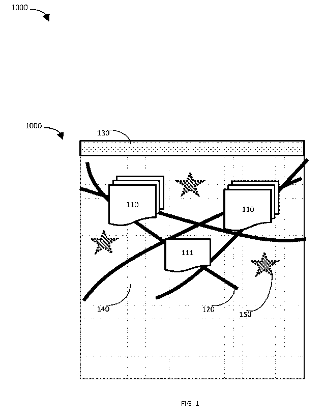
BRIEF DESCRIPTION OF THE DRAWINGS
[0009] The novel features of the disclosure are set forth with particularity
in the appended
claims. A better understanding of the features and advantages of the present
disclosure will be
obtained by reference to the following detailed description that sets forth
illustrative
embodiments, in which the principles of the disclosure are utilized, and the
accompanying
drawings of which:
[0010] FIG. 1 is a diagram of a conductive ink, per one or more embodiments,
herein;
[0011] FIG. 2A is a first optical microscope image of an exemplary first
conductive ink, per one
or more embodiments, herein;
100121 FIG. 2B is a second optical microscope image of an exemplary first
conductive ink, per
one or more embodiments, herein;
[0013] FIG. 3A is a particle size distribution of an exemplary first
conductive ink, per one or
more embodiments, herein;
[0014] FIG. 3B is an image of an exemplary first conductive ink on a HeDnan
gauge, per one or
more embodiments, herein;
[0015] FIG. 4A is an X-ray Diffraction graph of an exemplary first conductive
ink, per one or
more embodiments, herein;
[0016] FIG. 4B is a Raman Spectroscopy graph of an exemplary first conductive
ink, per one or
more embodiments, herein;
[0017] FIG. 5 is a shear rate vs viscosity graph of an exemplary first
conductive ink, per one or
more embodiments, herein;
[0018] FIG. 6A is an exemplary first graph of a thermal analysis of an
exemplary first
conductive ink, per one or more embodiments, herein;
[0019] FIG. 6B is an exemplary second graph of a thermal analysis of an
exemplary first
conductive ink, per one or more embodiments, herein;
[0020] FIG. 7 is an exemplary third graph of a thermal analysis of an
exemplary first conductive
ink, per one or more embodiments, herein;
[0021] FIG. 8A is a first SEM image of an exemplary second conductive ink, per
one or more
embodiments, herein;
[0022] FIG. 8B is a second SEM image of an exemplary second conductive ink,
per one or more
embodiments, herein;
- 4 -
CA 03236862 2024- 4- 30
WO 2023/081265
PCT/ITS2022/048788
[0023] FIG. 9A is a particle size distribution of an exemplary second
conductive ink, per one or
more embodiments, herein;
[0024] FIG. 9B is an image of an exemplary second conductive ink on a Hewnan
gauge, per one
or more embodiments, herein;
[0025] FIG. 10 is a Raman Spectroscopy graph of an exemplary second conductive
ink, per one
or more embodiments, herein;
[0026] FIG. 11A is a shear rate vs. viscosity graph of an exemplary second
conductive ink, per
one or more embodiments, herein;
[0027] FIG. 11B is an X-ray Diffraction graph of exemplary first and second
conductive inks,
per one or more embodiments, herein;
[0028] FIG. 12A is an exemplary first graph of a thermal analysis of an
exemplary second
conductive ink, per one or more embodiments, herein;
[0029] FIG. 12B is an exemplary second graph of a thermal analysis of an
exemplary second
conductive ink, per one or more embodiments, herein;
[0030] FIG. 13 is an exemplary third graph of a thermal analysis of an
exemplary second
conductive ink, per one or more embodiments, herein;
100311 FIG. 14A is a photograph of an exemplary conductive ink screen printed
onto a silicon
wafer, per one or more embodiments, herein;
[0032] FIG. 14B shows a photograph of traces of different widths of the
exemplary conductive
ink screen printed onto a silicon wafer and a high magnification photograph of
a trace, per one or
more embodiments, herein;
[0033] FIG. 15A is an optical profilometry image of the trace of FIG. 14A, per
one or more
embodiments, herein;
[0034] FIG. 15B is a three-dimensional rendering of the optical profilometry
image of FIG.
15A, per one or more embodiments, herein;
[0035] FIG. 16A is a graph of the height of optical profilometry image along a
first axis of the
trace of FIG. 15A, per one or more embodiments, herein;
[0036] FIG. 1 6R is a graph of the height of optical profilometry image along
a second axis of the
trace of FIG. 15A, per one or more embodiments, herein;
[0037] FIG. 17 is a graph of the conductivity vs the width of a trace formed
with an exemplary
conductive ink, per one or more embodiments, herein;
[0038] FIG. 18A is a graph of the dry thickness vs the sheet resistance of a
trace formed with an
exemplary conductive ink, per one or more embodiments, herein;
- 5 -
CA 03236862 2024- 4- 30
WO 2023/081265
PCT/ITS2022/048788
100391 FIG. 18B is a graph of the wet thickness vs dry thickness of a trace
formed with an
exemplary conductive ink, per one or more embodiments, herein;
100401 FIG. 19A is a graph of the wavelength transmittance of an exemplary
trace formed with
an exemplary conductive ink, per one or more embodiments, herein;
100411 FIG. 19B is a graph of the wavelength transmittance of an exemplary
conductive ink, per
one or more embodiments, herein;
100421 FIG. 20A is a first Scanning Electron Microscope (SEM) image of
exemplary reduced
graphene oxide sheets, per one or more embodiments, herein;
100431 FIG. 20B is a second SEM image of exemplary reduced graphene oxide
sheets, per one
or more embodiments, herein;
100441 FIG. 21A is a first Atomic Force Microscope (AFM) image of exemplary
reduced
graphene oxide sheets, per one or more embodiments, herein;
100451 FIG. 21B is a second AFM image of exemplary reduced graphene oxide
sheets, per one
or more embodiments, herein;
100461 FIG. 22A is a shear rate vs. viscosity graph of an exemplary third
conductive ink, per one
or more embodiments, herein;
100471 FIG. 22B is a torque vs. speed graph of the exemplary third conductive
ink, per one or
more embodiments, herein;
100481 FIG. 23A is a time vs. heat flow graph of the exemplary third
conductive ink, per one or
more embodiments, herein;
100491 FIG. 23B is a time vs. weight graph of the exemplary third conductive
ink, per one or
more embodiments, herein;
100501 FIG. 24A is an XRD pattern of a substrate coated with the exemplary
third conductive
ink, per one or more embodiments, herein;
100511 FIG. 24B is a Raman spectrum of a substrate coated with the exemplary
third conductive
ink, per one or more embodiments, herein;
100521 FIG. 25A is a dry film thickness vs. sheet resistance graph of a
substrate coated with the
exemplary third conductive ink, per one or more embodiments, herein;
100531 FIG. 25B is a wet film thickness vs. dry film thickness graph of a
substrate coated with
the exemplary third conductive ink, per one or more embodiments, herein,
100541 FIG. 26A is a particle distribution graph of the exemplary third
conductive ink, per one
or more embodiments, herein;
100551 FIG. 26B, shows a trace width vs. resistance for a substrate covered
with the exemplary
third conductive ink, per one or more embodiments, herein;
- 6 -
CA 03236862 2024- 4- 30
WO 2023/081265
PCT/ITS2022/048788
100561 FIG. 27A is a shear rate vs. viscosity graph of an exemplary fourth
conductive ink, per
one or more embodiments, herein;
100571 FIG. 27B is a torque vs. speed graph of the exemplary fourth conductive
ink, per one or
more embodiments, herein;
100581 FIG. 28A is a time vs. heat flow graph of an exemplary fourth
conductive ink, per one or
more embodiments, herein;
100591 FIG. 28B is a time vs. weight graph of the exemplary fourth conductive
ink, per one or
more embodiments, herein;
100601 FIG. 29A is an XRD graph of an exemplary fourth conductive ink, per one
or more
embodiments, herein;
100611 FIG. 29B is a Raman spectrum of the exemplary fourth conductive ink,
per one or more
embodiments, herein;
100621 FIG. 30A is a dry film thickness vs. sheet resistance graph of a
substrate coated with the
exemplary fourth conductive ink, per one or more embodiments, herein;
100631 FIG. 30B is a wet film thickness vs. dry film thickness graph of a
substrate coated with
the exemplary fourth conductive ink, per one or more embodiments, herein;
100641 FIG. 31 is a particle distribution graph of the exemplary fourth
conductive ink, per one or
more embodiments, herein;
100651 FIG. 32A is a shear rate vs. viscosity graph of an exemplary fifth
conductive ink, per one
or more embodiments, herein;
100661 FIG. 32B is a torque vs. speed graph of the exemplary fifth conductive
ink, per one or
more embodiments, herein;
100671 FIG. 33A is a time vs. heat flow graph of an exemplary fifth conductive
ink, per one or
more embodiments, herein;
100681 FIG. 33B is a time vs. weight graph of the exemplary fifth conductive
ink, per one or
more embodiments, herein;
100691 FIG. 34A is an XRD graph of an exemplary fifth conductive ink, per one
or more
embodiments, herein;
100701 FIG. 34B is a Raman spectrum of the exemplary fifth conductive ink, per
one or more
embodiments, herein;
100711 FIG. 35A is a particle distribution graph of the exemplary fifth
conductive ink, per one or
more embodiments, herein;
100721 FIG. 35B, shows a trace width vs. resistance for a substrate covered
with the exemplary
fifth conductive ink, per one or more embodiments, herein;
- 7 -
CA 03236862 2024- 4- 30
WO 2023/081265
PCT/ITS2022/048788
100731 FIG. 36A shows a first optical profilometry image of a substrate
covered with the
exemplary fifth conductive ink, per one or more embodiments, herein;
100741 FIG. 36B shows a graph of thickness of an exemplary dried fifth
conductive ink along the
length of the sample in FIG. 36A, per one or more embodiments, herein;
100751 FIG. 36C shows a graph of thickness of an exemplary dried fifth
conductive ink along
the width of the sample in FIG. 36A, per one or more embodiments, herein;
100761 FIG. 37A shows a second optical profilometry image of a substrate
covered with the
exemplary fifth conductive ink, per one or more embodiments, herein;
100771 FIG. 37B shows a third optical profilometry image of a substrate
covered with the
exemplary fifth conductive ink, per one or more embodiments, herein;
100781 FIG. 38A is a dry film thickness vs. sheet resistance graph of a
substrate coated with the
exemplary fifth conductive ink, per one or more embodiments, herein;
100791 FIG. 38B is a wet film thickness vs. dry film thickness graph of a
substrate coated with
the exemplary fifth conductive ink, per one or more embodiments, herein;
100801 FIG. 39A is a low magnification SEM image of a substrate coated with
the exemplary
fifth conductive ink, per one or more embodiments, herein;
100811 FIG. 39B is a high magnification SEM image of a substrate coated with
the exemplary
fifth conductive ink, per one or more embodiments, herein;
100821 FIG. 40A is a shear rate vs. viscosity graph of an exemplary sixth
conductive ink, per one
or more embodiments, herein;
100831 FIG. 40B is a torque vs. speed graph of the exemplary sixth conductive
ink, per one or
more embodiments, herein;
100841 FIG. 41A is a time vs. heat flow graph of the exemplary sixth
conductive ink, per one or
more embodiments, herein;
100851 FIG. 41B is a time vs. weight graph of the exemplary sixth conductive
ink, per one or
more embodiments, herein;
100861 FIG. 42A is an XRD pattern of a substrate coated with the exemplary
sixth conductive
ink, per one or more embodiments, herein;
100871 FIG. 42B is a Raman spectrum of a substrate coated with the exemplary
sixth conductive
ink, per one or more embodiments, herein;
100881 FIG. 43A is a particle distribution graph of the exemplary sixth
conductive ink, per one
or more embodiments, herein;
100891 FIG. 43Bis a dry film thickness vs. sheet resistance graph of a
substrate coated with the
exemplary sixth conductive ink, per one or more embodiments, herein;
- 8 -
CA 03236862 2024- 4- 30
WO 2023/081265
PCT/ITS2022/048788
[0090] FIG. 44A is a graph of the wet thickness vs dry thickness of a trace
formed with the
exemplary sixth conductive ink, per one or more embodiments, herein; and
[0091] FIG. 44B, shows a trace width vs. resistance for a substrate covered
with the exemplary
sixth conductive ink.
DETAILED DESCRIPTION
[0092] Currently, limited methods are available to manufacture printed
electronics due to the
limitations of conductive inks used therein. Current silver and copper-based
inks are often too
expensive for large scale device production. Further, such inks agglomerate
during printing to
form uneven and inconsistent components, have viscosities and surface tensions
that cannot be
tuned for specific printing methods, and suffer from poor adhesion to
substrates and low
flexibility. As such, economically manufacturing durable and highly conductive
printed
components with such inks is often difficult or ineffective.
[0093] To improve the performance of such printed electronics and to enable
the fabrication of a
broader range of such electronics, improved inks are required. As such,
provided herein are
conductive inks and methods of formulation thereof, whose electric and
mechanical properties
(e.g. viscosity and surface tension) enable its use in a wide array of
printing techniques. The
outstanding conductivity, thermal stability, chemical stability, and
flexibility of graphene in the
inks herein enable the production of low-cost electronics with tunable
electrochemical properties.
Finally, while many current conductive inks require multiple layers for proper
adhesion and
conductibility, the inks herein can form electronic circuits with sufficient
thickness using a
reduced number of layers such as even in a single print.
Conductive Inks
[0094] FIG. 1A is a diagram of a conductive ink 1000. In some embodiments, the
conductive ink
1000 comprises graphene 110, a binder 120, a stabilizer 130, and a solvent
140. In some
embodiments, the conductive ink 1000 consists of graphene 110, a binder 120, a
stabilizer 130,
and a solvent 140. In some embodiments, the conductive ink 1000 consists
essentially of
graphene 110, a binder 120, a stabilizer 130, and a solvent 140. In some
embodiments, the
conductive ink 1000 does not comprise a surfactant. In some embodiments, the
conductive ink
1000 does not comprise a defoamer.
[0095] The specific components of the conductive ink 1000 herein enable its
unexpectedly
improved elasticity, adhesion, thermal stability, coating uniformity, chemical
stability, and
tunable viscosity. The ink exhibits superior stability and coats evenly
without leaving holes and
has a smooth surface.
- 9 -
CA 03236862 2024- 4- 30
WO 2023/081265
PCT/ITS2022/048788
100961 In some embodiments, the graphene 110 comprises reduced graphene oxide.
In some
embodiments, the graphene 110 comprises activated reduced graphene oxide. In
some
embodiments, at least about 85%, 86%, 87%, 88%, 89%, 90%, 91 %, 92%, 93%, 94%,
95
%, 96 %, 97 %, 98% or more of the graphene 110 sheets consist of a single
layer of graphene
111. In some embodiments, the high content of single layer graphene sheets 111
within the
conductive ink 1000 improves the conductivity of the conductive ink 1000 when
dry. In some
embodiments, a percentage of the reduced graphene oxide that consists of a
single layer is
determined by atomic force microscopy (AFM). In some embodiments, the graphene
sheets 110
have an oxygen content of at most about 2 %, 3 %, 4 %, 5 %, 6 %, 7 %, 8 %, 9
%, or 10 %,
including increments therein. In some embodiments, the low oxygen content of
the graphene
sheets 110 within the conductive ink 1000 improves the conductivity of the
conductive ink 1000
when dry.
100971 In some embodiments, the binder 120 is a polymeric binder 120. In some
embodiments,
the polymeric binder 120 is a thermoplastic copolymer. In some embodiments,
the binder 120
comprises polyvinylpyrrolidone, ethyl methacrylate, butyl methacrylate, or any
combination
thereof. The specific binders 120 herein enable the unexpectedly improved
elasticity, adhesion,
thermal stability, chemical stability, and tunable viscosity of the conductive
inks 1000 herein and
electronics formed therefrom.
100981 In some embodiments, the stabilizer 130 comprises a polymer. In some
embodiments, the
stabilizer 130 is solid at room temperature. In some embodiments, the
stabilizer 130 comprises
polytetrahydrofuran, fluorinated triethylene glycol monomethyl ether, ethyl
cellulose, diethylene
glycol, or any combination thereof The specific stabilizers 130 herein provide
the inks 1000
herein unexpectedly improved ability to uniform coating of a substrate, to dry
slowly and prevent
cracking and island formation, to stabilize the graphene 110 within the ink
1000 to prevent
agglomeration, and to elastically bend without damage. In some embodiments,
the stabilizer 130
comprises polytetrahydrofuran, which increase s the viscosity, flexibility,
and elasticity of the
conductive ink 1000, stabilizes the graphene 110 in the conductive ink 1000,
and slows down the
drying process at room temp to prevent cracking and island formation In some
embodiments, the
stabilizer 130 comprises diethylene glycol, which improves the flexibility and
strength of the
dried conductive ink 1000.
100991 In some embodiments, the solvent 140 comprises propylene glycol n-
propyl ether, 2-
ethyl-l-hexanol, diethylene glycol monobutyl ether, 2-ethyl-I -butanol, 2-
methy1-1-pentanol,
propylene glycol monomethyl ether acetate, hexamine, cycloheptylamine, isoamyl
amine, 3 -
methoxypropylamine, parachlorobenzotrifluoride, ethylene glycol, isopropanol,
ethyl acetate,
- 10 -
CA 03236862 2024- 4- 30
WO 2023/081265
PCT/ITS2022/048788
chloroform, dimethylformamide, n-methy1-2-pyrrolidone, tetrahydrofuran, and
dichlorobenzene,
or any combination thereof. In some embodiments, the wax is an animal wax, a
vegetable wax, a
mineral wax, a petroleum wax, or any combination thereof. In some embodiments,
the solvent
140 increases the stability of the graphene 110 within the inks 1000 herein.
In some
embodiments, the solvent 140 is volatile. In some embodiments, the solvent 140
has a vapor
pressure at 20 C of about 20 Pa to about 250 Pa. In some embodiments, the
solvent 140 has a
boiling point of about 110 C to about 200 C. In some embodiments, the vapor
pressure and the
boiling point of the solvent enable the inks 1000 herein to dry slowly and
thus prevent cracking.
In some embodiments, the high boiling point of the solvent increases the
drying time of the
conductive ink, increases the time for coating a substrate with the conductive
ink, and may
permit for even drying of the conductive ink across the surface of the ink
applied to the substrate.
In some embodiments, the even drying of the ink across the surface of the ink
applied to the
substrate may prevent the edges from drying may prevent the edges from drying
prior to the bulk
of the conductive ink, and may prevent capillary flow of suspend reduced
graphene oxide
particles outward from the bulk of the conductive ink to the edges of the
conductive ink as
applied to the substrate, and may permit for an even coating of the conductive
ink on a substrate
with a uniform or substantially uniform dispersion of graphene oxide particles
throughout the
conductive ink applied to the substrate. In some embodiments, the slow, even
drying of the ink
across the surface of the ink applied to the substrate may allow for a highly
uniform coating of
the conductive ink applied to a substrate, improving the conductivity of the
final product
produced with the conductive ink applied to a substrate.
[0100] In some embodiments, the conductive ink has a particle size of about 3
um to about 20
um. In some embodiments, the conductive ink has a particle size of about 3 um
to about 4 um,
about 3 urn to about 6 urn, about 3 urn to about 8 urn, about 3 urn to about
10 urn, about 3 urn to
about 12 um, about 3 um to about 14 um, about 3 um to about 16 um, about 3 um
to about 18 um,
about 3 um to about 20 um, about 4 um to about 6 um, about 4 um to about 8 um,
about 4 urn to
about 10 um, about 4 um to about 12 um, about 4 um to about 14 um, about 4 um
to about 16 um,
about 4 urn to about 18 urn, about 4 urn to about 20 urn, about 6 urn to about
S urn, about 6 um to
about 10 um, about 6 um to about 12 um, about 6 um to about 14 urn, about 6 um
to about 16 um,
about 6 um to about 18 um, about 6 um to about 20 um, about 8 um to about 10
um, about 8 um
to about 12 urn, about 8 urn to about 14 urn, about 8 urn to about 16 urn,
about 8 urn to about 18
um, about 8 um to about 20 um, about 10 um to about 12 um, about 10 um to
about 14 um, about
urn to about 16 urn, about 10 urn to about 18 urn, about 10 urn to about 20
urn, about 12 urn to
about 14 um, about 12 um to about 16 um, about 12 um to about 18 um, about 12
um to about 20
- 11 -
CA 03236862 2024- 4- 30
WO 2023/081265
PCT/ITS2022/048788
um, about 14 um to about 16 um, about 14 um to about 18 urn, about 14 um to
about 20 um,
about 16 um to about 18 um, about 16 um to about 20 um, or about 18 urn to
about 20 urn,
including increments therein. In some embodiments, the conductive ink has a
particle size of
about 3 um, about 4 um, about 6 um, about 8 um, about 10 um, about 12 um,
about 14 um, about
16 um, about 18 um, or about 20 um. In some embodiments, the conductive ink
has a particle
size of at least about 3 urn, about 4 urn, about 6 urn, about 8 urn, about 10
urn, about 12 urn,
about 14 um, about 16 um, or about 18 um. In some embodiments, the conductive
ink has a
particle size of at most about 4 urn, about 6 um, about 8 um, about 10 um,
about 12 um, about 14
um, about 16 um, about 18 um, or about 20 um. In some embodiments, the
specific particle sizes
of the inks herein provide a tunable viscosity and surface tension to enable
printing with a variety
of methods and machines for production of a wide array of electronic
components. In some
embodiments, the above-described particle sizes refer a mean or average
particle size. In some
embodiments, the above-described particle sizes refer to at least 80%, at
least 90%, or at least
95% of the ink having the recited particle size.
101011 The viscosity of the conductive ink can be tuned by adjusting the shear
mixing time,
wherein longer shearing times reduce viscosity. In some embodiments, the
conductive ink has a
viscosity of about 25 cP to about 3,000 cP. In some embodiments, the
conductive ink has a
viscosity of about 25 cP to about 50 cP, about 25 cP to about 100 cP, about 25
cP to about 250
cP, about 25 cP to about 500 cP, about 25 cP to about 750 cP, about 25 cP to
about 1,000 cP,
about 25 cP to about 2,000 cP, about 25 cP to about 3,000 cP, about 25 cP to
about 400 cP, about
50 cP to about 100 cP, about 50 cP to about 250 cP, about 50 cP to about 500
cP, about 50 cP to
about 750 cP, about 50 cP to about 1,000 cP, about 50 cP to about 2,000 cP,
about 50 cP to about
3,000 cP, about 50 cP to about 400 cP, about 100 cP to about 250 cP, about 100
cP to about 500
cP, about 100 cP to about 750 cP, about 100 cP to about 1,000 cP, about 100 cP
to about 2,000
cP, about 100 cP to about 3,000 cP, about 100 cP to about 400 cP, about 250 cP
to about 500 cP,
about 250 cP to about 750 cP, about 250 cP to about 1,000 cP, about 250 cP to
about 2,000 cP,
about 250 cP to about 3,000 cP, about 250 cP to about 400 cP, about 500 cP to
about 750 cP,
about 500 cP to about 1,000 cP, about 500 cP to about 2,000 cP, about 500 cP
to about 3,000 cP,
about 500 cP to about 400 cP, about 750 cP to about 1,000 cP, about 750 cP to
about 2,000 cP,
about 750 cP to about 3,000 cP, about 750 cP to about 400 cP, about 1,000 cP
to about 2,000 cP,
about 1,000 cP to about 3,000 cP, about 1,000 cP to about 400 cP, about 2,000
cP to about 3,000
cP, about 2,000 cP to about 400 cP, or about 3,000 cP to about 400 cP,
including increments
therein. In some embodiments, the conductive ink has a viscosity of about 25
cP, about 50 cP,
about 100 cP, about 250 cP, about 500 cP, about 750 cP, about 1,000 cP, about
2,000 cP, about
- 12 -
CA 03236862 2024- 4- 30
WO 2023/081265
PCT/ITS2022/048788
3,000 cP, or about 400 cP. In some embodiments, the conductive ink has a
viscosity of at least
about 25 cP, about 50 cP, about 100 cP, about 250 cP, about 500 cP, about 750
cP, about 1,000
cP, about 2,000 cP, or about 3,000 cP. In some embodiments, the conductive ink
has a viscosity
of at most about 50 cP, about 100 cP, about 250 cP, about 500 cP, about 750
cP, about 1,000 cP,
about 2,000 cP, about 3,000 cP, or about 400 cP. In some embodiments, the
viscosity of the inks
herein enable its printing with a variety of methods and machines, to produce
a wide array of
electronic components.
101021 In some embodiments, the conductive ink has a shear rate of about 100 s-
1 to about 400 s-
1. In some embodiments, the conductive ink has a shear rate of about 100 s-1
to about 150 s-1,
about 100 s-1 to about 200 s-1, about 100 s-1 to about 250 s-1, about 100 s-1
to about 300 s-1,
about 100 s-1 to about350 s-1, about 100 s-1 to about 400 s-1, about 150 s-1
to about 200 s-1,
about 150 s-1 to about 250 s-1, about 150 s-1 to about 300 s-1, about 150 s-1
to about350 s-1,
about 150 s-1 to about 400 s-1, about 200 s-1 to about 250 s-1, about 200 s-1
to about 300 s-1,
about 200 s-1 to about350 s-1, about 200 s-1 to about 400 s-1, about 250 s-1
to about 300 s-1,
about 250 s-1 to about350 s-1, about 250 s-1 to about 400 s-1, about 300 s-1
to about 350 s-1,
about 300 s-1 to about 400 s-1, or about 350 s-1 to about 400 s-1, including
increments therein.
In some embodiments, the conductive ink has a shear rate of about 100 s-1,
about 150 s-1, about
200 s-1, about 250 s-1, about 300 s-1, about 350 s-1, or about 400 s-1. In
some embodiments, the
conductive ink has a shear rate of at least about 100 s-1, about 150 s-1,
about 200 s-1, about 250
s-1, about 300 s-1, or about 350 s-1. In some embodiments, the conductive ink
has a shear rate of
at most about 150 s-1, about 200 s-1, about 250 s-1, about 300 s-1, about 350
s-1, or about 400 s-
1. In some embodiments, the shear rate of the inks herein enable its printing
with a variety of
methods and machines, to produce a wide array of electronic components.
101031 In some embodiments, the conductive ink, when wet, has a w/w
concentration of the
graphene of about 0.1 % to about 10 %. In some embodiments, the conductive
ink, when wet, has
a w/w concentration of the graphene of about 0.1 c)/0 to about 0.5 %, about
0.1 % to about 1 %,
about 0.1 % to about 2 %, about 0.1% to about 3 %, about 0.1 % to about 4 %,
about 0.1% to
about 5 %, a.b out 0.1 % to about 6 %, about 0.1 % to about 7 %, a.b out 0.1%
to about 8 %, about
0.1 % to about 9%, about 0.1 % to about 10 %, about 0.5% to about 1 %, about
0.5 % to about 2
%, about 0.5 % to about 3 %, about 0.5% to about 4 %, about 0.5 % to about 5
%, about 0.5% to
about 6%, about 0.5 % to about 7 %, about 0.5 % to about 8 %, about 0.5% to
about 9 %, about
0.5% to about 10%, about 1 % to about 2%, about 1 % to about 3%, about 1 % to
about 4%,
about 1 % to about 5 %, about 1 % to about 6 %, about 1 % to about 7 %, about
1 % to about 8
%, about 1 % to about 9 %, about 1 % to about 10 %, about 2 % to about 3 %,
about 2 % to about
- 13 -
CA 03236862 2024- 4- 30
WO 2023/081265
PCT/ITS2022/048788
4%, about 2 % to about 5%, about 2 % to about 6 %, about 2 % to about 7%,
about 2 % to
about 8 %, about 2 % to about 9 %, about 2 % to about 10 %, about 3 % to about
4 %, about 3 %
to about 5 %, about 3 % to about 6 %, about 3 % to about 7 %, about 3 % to
about 8 %, about 3
% to about 9%, about 3 % to about 10 %, about 4% to about 5 %, about 4% to
about 6 %, about
4 % to about 7 %, about 4 % to about 8 %, about 4 % to about 9 %, about 4 % to
about 10 %,
about 5 % to about 6 %, about 5 % to about 7 %, about 5 % to about 8 %, about
5 % to about 9
%, about 5 % to about 10 %, about 6 % to about 7 %, about 6 % to about 8 %,
about 6 % to about
9%, about 6% to about 10%, about 7% to about 8%, about 7% to about 9%, about
7% to
about 10 %, about 8 % to about 9 %, about 8 % to about 10 %, or about 9 % to
about 10 %,
including increments therein. In some embodiments, the conductive ink, when
wet, has a w/w
concentration of the graphene of about 0.1 %, about 0.5 %, about 1 %, about 2
%, about 3 %,
about 4 %, about 5%, about 6%, about 7%, about 8 %, about 9%, or about 10%. In
some
embodiments, the conductive ink, when wet, has a w/w concentration of the
graphene of at least
about 0.1 %, about 0.5 %, about 1%, about 2 %, about 3 %, about 4 %, about 5%,
about 6 %,
about 7 %, about 8 %, or about 9 %. In some embodiments, the conductive ink,
when wet, has a
w/w concentration of the graphene of at most about 0.5 %, about 1%, about 2 %,
about 3 %,
about 4 %, about 5 %, about 6 %, about 7 %, about 8 %, about 9 %, or about 10
%. In some
embodiments, the low concentration of the graphene oxide herein, in addition
to the additional
elements of the conductive ink, reduces the cost of the conductive inks herein
while maintaining
a high conductivity and low resistance.
101041 In some embodiments, the conductive ink, when wet, has a w/w
concentration of the
binder of about 10 % to about 60 %. In some embodiments, the conductive ink,
when wet, has a
w/w concentration of the binder of about 10 A to about 15 `)/0, about 10 % to
about 20%, about
-I 0 % to about 25 %, about -I 0 % to about 30 %, about -10 % to about 35 %,
about -10 % to about
40 %, about 10 % to about 45 %, about 10 % to about 50 %, about 10% to about
55 %, about 10
% to about 60 %, about 15 % to about 20 %, about 15 % to about 25 %, about 15
% to about 30
%, about 15 % to about 35 %, about 15 % to about 40 %, about 15 % to about 45
%, about 15 %
to about 50%, about 15% to about 55%, about 15 % to about 60%, about 20% to
about 25 %,
about 20 % to about 30 %, about 20 % to about 35 %, about 20 % to about 40%,
about 20 % to
about 45%, about 20% to about 50%, about 20% to about 55%, about 20% to about
60%,
about 25 % to about 30%, about 25% to about 35%, about 25% to about 40%, about
25 % to
about 45 %, about 25 % to about 50 %, about 25 % to about 55 %, about 25 % to
about 60 %,
about 30% to about 35 %, about 30% to about 40%, about 30% to about 45 %,
about 30% to
about 50 %, about 30 % to about 55 %, about 30 % to about 60 %, about 35 % to
about 40%,
- 14 -
CA 03236862 2024- 4- 30
WO 2023/081265
PCT/ITS2022/048788
about 35 % to about 45 %, about 35 % to about 50 %, about 35 % to about 55 %,
about 35 % to
about 60%, about 40% to about 45 %, about 40% to about 50%, about 40% to about
55%,
about 40 % to about 60 %, about 45 % to about 50 %, about 45 % to ab out 55 %,
about 45 % to
about 60%, about 50% to about 55%, about 50% to about 60%, or about 55 % to
about 60%,
including increments therein. In some embodiments, the conductive ink, when
wet, has a w/w
concentration of the binder of about 10%, about 15 %, about 20 %, about 25 %,
about 30 %,
about 35%, about 40%, about 45 %, about 50%, about 55%, or about 60 %. In some
embodiments, the conductive ink, when wet, has a w/w concentration of the
binder of at least
about 10%, about 15%, about 20 %, about 25 %, about 30 %, about 35 %, about 40
%, about 45
%, about 50 %, or about 55 %. In some embodiments, the conductive ink, when
wet, has a w/w
concentration of the binder of at most about 15%, about 20 %, about 25 %,
about 30 %, ab out 35
%, about 40 %, about 45 %, about 50 %, about 55 %, or about 60 %. The specific
w/w
concentrations of the binder herein improve the elasticity, adhesion, thermal
stability, and
chemical stability of the inks herein, while maintaining tunable viscosities
and surface tensions.
101051 In some embodiments, the conductive ink, when wet, has a w/w
concentration of the
stabilizer of about 1 % to about 80 %. In some embodiments, the conductive
ink, when wet, has a
w/w concentration of the stabilizer of about 1 % to about 5 %, about 1 % to
about 10 %, about 1
% to about 15 %, about 1 % to about 20 %, about 1 % to about 25 %, about 1 %
to about 30 %,
about 1 % to about 40 %, about 1 % to about 50 %, about 1 % to about 60 %,
about 1 % to about
70%, about 1 % to about 80%, about 5% to about 10 %, about 5% to about 15 %,
about 5 % to
about 20 %, about 5 % to about 25 %, about 5 % to about 30 %, about 5 % to
about 40 %, about
% to about 50%, about 5 % to about 60 %, about 5 % to about 70 %, about 5 % to
about 80 %,
about 10 % to about 15%, about 10 % to about 20%, about 10 % to about 25 %,
about 10 % to
about 30 %, about I 0 % to about 40 %, about I 0 % to about 50 %, about I 0 %
to about 60 %,
about 10 % to about 70 %, about 10 % to about 80 %, about 15 % to about 20 %,
about 15 % to
about 25%, about 15% to about 30 %, about 15% to about 40%, about 15% to about
50%,
about 15 % to about 60 %, about 15 % to about 70 %, about 15 % to about 80 %,
about 20 % to
about 25%, about 20 % to about 30 %, about 20% to about 40 %, about 20 % to
about 50 %,
about 20 % to about 60 %, about 20 % to about 70 %, about 20 % to about 80 %,
about 25 % to
about 30%, about 25 % to about 40 %, about 25 % to about 50%, about 25 % to
about 60%,
about 25 % to about 70 %, about 25 % to about 80 %, about 30 % to about 40 %,
about 30 % to
about 50%, about 30% to about 60%, about 30% to about 70%, about 30% to about
80%,
about 40 % to about 50 %, about 40 % to about 60 %, about 40 % to about 70 %,
about 40 % to
about 80 %, about 50% to about 60 %, about 50 % to about 70 %, about 50 % to
about 80 %,
- 15 -
CA 03236862 2024- 4- 30
WO 2023/081265
PCT/ITS2022/048788
about 60 % to about 70 %, about 60 % to about 80 %, or about 70 % to about
80%, including
increments therein. In some embodiments, the conductive ink, when wet, has a
w/w
concentration of the stabilizer of about 1%, about 5%, about 10%, about 15%,
about 20 %,
about 25 %, about 30 %, about 40 %, about 50 %, about 60 %, about 70 %, or
about 80 %. In
some embodiments, the conductive ink, when wet, has a w/w concentration of the
stabilizer of at
least about 1 %, about 5%, about 10%, about 15%, about 20%, about 25%, about
30%, about
40 %, about 50 %, about 60 %, or about 70 %. In some embodiments, the
conductive ink, when
wet, has a w/w concentration of the stabilizer of at most about 5 %, about
10%, about 15 %,
about 20 %, about 25 %, about 30 %, about 40 %, about 50 %, about 60 %, about
70 %, or about
80 %. Various w/w concentrations of the stabilizer disclosed herein can
improve the ink's ability
for uniform coating on a substrate while preventing cracking and island
formation, and stabilizes
the graphene within the ink to prevent agglomeration, while maintaining
tunable viscosities and
surface tensions. In some embodiments, w/w concentrations of the stabilizer
herein increases the
drying time of the conductive ink, increases the time for coating a substrate
with the conductive
ink, and may permit for even drying of the conductive ink across the surface
of the ink applied to
the substrate. In some embodiments, the even drying of the ink across the
surface of the ink
applied to the substrate may prevent the edges from drying may prevent the
edges from drying
prior to the bulk of the conductive ink, and may prevent capillary flow of
suspend reduced
graphene oxide particles outward from the bulk of the conductive ink to the
edges of the
conductive ink as applied to the substrate, and may permit for an even coating
of the conductive
ink on a substrate with a uniform or substantially uniform dispersion of
graphene oxide particles
throughout the conductive ink applied to the substrate. In some embodiments,
the slow, even
drying of the ink across the surface of the ink applied to the substrate may
allow for a highly
uniform coating of the conductive ink applied to a substrate, improving the
conductivity of the
final product produced with the conductive ink applied to a substrate.
101061 In some embodiments, a ratio between the polytetrahydrofuran and the
diethylene glycol
is about 8:1 to about 11:1. In some embodiments, a ratio b etween the
polytetrahydrofuran and the
diethyl en e glycol is about Si to about 8.51, about Si to a.b out 91, about
Si to a.b out 9.51,
about 8:1 to about 10:1, about 8:1 to about 10.5:1, about 8:1 to about 11:1,
about 8.5:1 to about
9:1, about 8.5:1 to about 9.5:1, about 8.5:1 to about 10:1, about 8.5:1 to
about 10.5:1, about 8.5:1
to about 11:1, about 9:1 to about 9.5:1, about 9:1 to about 10:1, about 9:1 to
about 10.5:1, about
9:1 to about 11:1, about 9.5:1 to about 10:1, about 9.5:1 to about 10.5:1,
about 9.5:1 to about
11:1, about 10:1 to about 10.5:1, about 10:1 to about 11:1, or about 10.5:1 to
about 11:1,
including increments therein. In some embodiments, a ratio between the
polytetrahydrofuran and
- 16 -
CA 03236862 2024- 4- 30
WO 2023/081265
PCT/ITS2022/048788
the diethylene glycol is about 8:1, about 8.5:1, about 9:1, about 9.5:1, about
10:1, about 10.5:1,
or about 11:1. In some embodiments, a ratio between the polytetrahydrofuran
and the diethylene
glycol is at least about 8:1, about 8.5:1, about 9:1, about 9.5:1, about 10:1,
or about 10.5:1. In
some embodiments, a ratio between the polytetrahydrofuran and the diethylene
glycol is at most
about 8.5:1, about 9:1, about 9.5:1, about 10:1, about 10.5:1, or about 11:1.
101071 In some embodiments, the conductive ink, when wet, has a w/w
concentration of the
solvent of about 20% to about 90%. In some embodiments, the conductive ink,
when wet, has a
w/w concentration of the solvent of about 20 % to about 30 %, about 20 % to
about 40%, about
20 % to about 50 %, about 20 % to about 60 %, about 20 % to about 70 %, about
20 % to about
80 %, about 20 % to about 90 %, about 30 % to about 40 %, about 30 % to about
50 %, about 30
% to about 60 %, about 30 % to about 70 %, about 30 % to about 80 %, about 30
% to about 90
%, about 40 % to about 50 %, about 40 % to about 60 %, about 40 % to about 70
%, about 40 %
to about 80 %, about 40 % to about 90 %, about 50 % to about 60 %, about 50 %
to about 70 %,
about 50 % to about 80 %, about 50 % to about 90 %, about 60 % to about 70 %,
about 60 % to
about 80 %, about 60% to about 90%, about 70 % to about 80 %, about 70 % to
about 90%, or
about 80 % to about 90 %, including increments therein. In some embodiments,
the conductive
ink, when wet, has a w/w concentration of the solvent of about 20 %, about 30
%, about 40 %,
about 50 %, about 60 %, about 70 %, about 80 %, or about 90 %. In some
embodiments, the
conductive ink, when wet, has a w/w concentration of the solvent of at least
about 20 %, about 30
%, about 40 %, about 50 %, about 60 %, about 70 %, or about 80 %. In some
embodiments, the
conductive ink, when wet, has a w/w concentration of the solvent of at most
about 30 %, about
40 %, about 50 %, about 60 %, about 70%, about 80 %, or about 90 %. The
specific w/w
concentrations of the solvent herein unexpectedly improve the stability of the
graphene within
the inks, while maintaining tunable viscosities and surface tensions.
101081 In some embodiments, the conductive ink 1000 further comprises a
conductive additive
150. In some embodiments, the conductive additive 150 comprises a nanocarbon.
In some
embodiments, the nanocarbon comprises carbon nanoparticles, carbon nanodots,
carbon
n an otubes, graphene nanoribbons, carbon nanofibers, nanographite, carbon
onions, carbon
nanocones, or any combination thereof. In some embodiments, the conductive
additives 150
herein improve the conductivity of the inks 2000 herein, while maintaining its
rheological
properties to enable printing through various means to form a wide array of
electronic
components. In some embodiments, the conductive additives 150 herein improve
the electronic
conductivity of the ink and lower overall viscosity to match the requirement
for micro-gravure
printing. In some embodiments, the carbon nanoparticles comprise carbon black.
- 17 -
CA 03236862 2024- 4- 30
WO 2023/081265
PCT/ITS2022/048788
101091 In some embodiments, the conductive ink, when wet, has a w/w
concentration of the
conductive additive of about 1 % to about 40%. In some embodiments, the
conductive ink, when
wet, has a w/w concentration of the conductive additive of about 1 % to about
5 %, about 1 % to
about 10 %, about 1 % to about 15 %, about 1 % to about 20 %, about 1 % to
about 25 %, about
1 % to about 30 %, about 1 % to about 35 %, about 1 % to about 40 %, about 5 %
to about 10 %,
about 5 % to about 15 %, about 5 % to about 20 %, about 5 % to about 25 %,
about 5 % to about
30 %, about 5 % to about 35 %, about 5 % to about 40 %, about 10 % to about 15
%, about 10 %
to about 20 %, about 10 % to about 25 %, about 10 % to about 30 %, about 10 %
to about 35 %,
about 10 % to about 40 %, about 15 % to about 20 %, about 15 % to about 25 %,
about 15 % to
about 30%, about 15 % to about 35 %, about 15% to about 40 %, about 20% to
about 25 %,
about 20 % to about 30 %, about 20 % to about 35 %, about 20 % to about 40 %,
about 25 % to
about 30%, about 25% to about 35 %, about 25% to about 40%, about 30% to about
35%,
about 30 % to about 40 %, or about 35 % to about 40 %, including increments
therein. In some
embodiments, the conductive ink, when wet, has a w/w concentration of the
conductive additive
of about 1 %, about 5 %, about 10 %, about 15 %, about 20 %, about 25 %, ab
out 30 %, about 35
%, or about 40 %. In some embodiments, the conductive ink, when wet, has a w/w
concentration
of the conductive additive of at least about 1 %, about 5%, about 10%, about
15 %, about 20 %,
about 25 %, about 30 %, or about 35 %. In some embodiments, the conductive
ink, when wet,
has a w/w concentration of the conductive additive of at most about 5 %, about
10 %, about 15
%, about 20 %, about 25 %, about 30 %, about 35 %, or about 40 %.
Characterization of Conductive Inks
101101 The conductive inks herein exhibit level 5B adhesion (ideal adhesion),
enabling its use on
a wide array of substrates, such as, for example Polyimide, glass, aluminum,
and polyethylene
terephthalate. Further, while the components in many current conductive inks
separate and form
non-dispersible clumps, the conductive inks herein exhibit a shelf life of
over 1 year, wherein the
components of the ink remain in solution. Further, unlike many current
conductive inks, the
conductive inks herein inks can be produced and supplied in large volumes.
Additionally, the
conductive inks herein improve the efficiency and speed of forming printed
conductive materials,
as they can be cured at any temperature, and at curing times as low as 10
minutes or less at
temperatures below 110 C. Finally, the conductive inks herein are water
soluble, and produce
consistent continuous coatings when dried.
101111 In some embodiments, the conductive ink has a solid content of about 5%
to about 80%.
In some embodiments, the conductive ink has a solid content of about 5 % to
about 10 %, about 5
- 18 -
CA 03236862 2024- 4- 30
WO 2023/081265
PCT/ITS2022/048788
% to about 20 %, about 5 % to ab out 30 %, about 5 % to about 40 %, about 5 %
to about 50 %,
about 5 % to about 60 %, about 5 % to about 70 %, about 5 % to about 80 %,
about 10% to
about 20 %, about 10% to about 30 %, about 10% to about 40 %, about 10% to
about 50 %,
about 10% to about 60 %, about 10% to about 70 %, about 10% to about 80%,
about 20 % to
about 30%, about 20% to about 40 %, about 20% to about 50%, about 20% to about
60%,
about 20 % to about 70 %, about 20 % to about 80 %, ab out 30 % to about 40 %,
ab out 30 % to
about 50 %, about 30 % to about 60 %, about 30 % to about 70 %, about 30 % to
about 80 %,
about 40 % to about 50 %, about 40 % to about 60 %, about 40 % to about 70 %,
about 40 % to
about 80 %, about 50% to about 60%, about 50% to about 70%, about 50 % to
about 80%,
about 60 % to about 70 %, about 60 % to about 80 %, or about 70 % to about
80%, including
increments therein. In some embodiments, the conductive ink has a solid
content of about 5 %,
about 10%, about 20 %, about 30 %, about 40 %, about 50 %, about 60 %, about
70 %, or about
80 %. In some embodiments, the conductive ink has a solid content of at least
about 5 %, about
%, about 20 %, about 30 %, about 40%, about 50 %, about 60 %, or about 70 %.
In some
embodiments, the conductive ink has a solid content of at most about 10 %,
about 20%, about 30
%, about 40 %, about 50 %, about 60 %, about 70 %, or about 80 %.
101121 In some embodiments, a ratio between a wet thickness of the conductive
ink dispersed on
a substrate and a dry thickness of the conductive ink dried on the substrate
is about 2:1 to about
6:1. In some embodiments, a ratio between a wet thickness of the conductive
ink dispersed on a
substrate and a dry thickness of the conductive ink dried on the substrate is
about 2:1 to about
2.5:1, about 2:1 to about 3:1, about 2:1 to about 3.5:1, about 2:1 to about
4:1, about 2:1 to about
4.5:1, about 2:1 to about 5:1, about 2:1 to about 5.5:1, about 2:1 to about
6:1, about 2.5:1 to about
3:1, about 2.5:1 to about 3.5:1, about2.5:1 to about 4:1, about 2.5:1 to
about4.5:1, about 2.5:1 to
about 5: I , about 2.5: I to about 5.5: I , about 2.5: I to about 6: I , about
3: I to ab out 3.5: I , about 3: I
to about 4:1, about 3:1 to about 4.5:1, about 3:1 to about 5:1, about 3:1 to
about 5.5:1, about 3:1
to about 6:1, about 3.5:1 to about 4:1, about 3.5:1 to about 4.5:1, about
3.5:1 to about 5:1, about
3.5:1 to about 5.5:1, about 3.5:1 to about 6:1, about 4:1 to about 4.5:1,
about 4:1 to about 5:1,
about 41 to about 5.51, about 41 to about 61, a.bout 4.51 to about 51, about
4.51 to about
5.5:1, about 4.5:1 to about 6:1, about 5:1 to about 5.5:1, about 5:1 to about
6:1, or about 5.5:1 to
about 6:1, including increments therein. In some embodiments, a ratio between
a wet thickness of
the conductive ink dispersed on a substrate and a dry thickness of the
conductive ink dried on the
substrate is about2:1, about2.5:1, about 3:1, about 3.5:1, about4:1,
about4.5:1, about 5:1, about
5.5:1, or about 6:1. In some embodiments, a ratio between a wet thickness of
the conductive ink
dispersed on a substrate and a dry thickness of the conductive ink dried on
the substrate is at least
- 19 -
CA 03236862 2024- 4- 30
WO 2023/081265
PCT/ITS2022/048788
about 2:1, about 2.5:1, about 3:1, about 3.5:1, about 4:1, about 4.5:1, about
5:1, or about 5.5:1. In
some embodiments, a ratio between a wet thickness of the conductive ink
dispersed on a
substrate and a dry thickness of the conductive ink dried on the substrate is
at most about 2.5:1,
about3:1, about3.5:1, about 4:1, about 4.5:1, about 5:1, about 5.5:1, or about
6:1.
101131 In some embodiments, the conductive ink has a resistance when dry of
about 300 ohm/sq
to about 80,000 ohm/sq. In some embodiments, the conductive ink has a
resistance when dry of
about 300 ohm/sq to about 500 ohm/sq, about 300 ohm/sq to about 750 ohm/sq,
about 300
ohm/sq to about 1,000 ohm/sq, about 300 ohm/sq to about 2,500 ohm/sq, about
300 ohm/sq to
about 5,000 ohm/sq, about 300 ohm/sq to about 7,500 ohm/sq, about 300 ohm/sq
to about 10,000
ohm/sq, about 300 ohm/sq to about 25,000 ohm/sq, about 300 ohm/sq to about
50,000 ohm/sq,
about 300 ohm/sq to about 80,000 ohm/sq, about 500 ohm/sq to about 750 ohm/sq,
about 500
ohm/sq to about 1,000 ohm/sq, about 500 ohm/sq to about 2,500 ohm/sq, about
500 ohm/sq to
about 5,000 ohm/sq, about 500 ohm/sq to about 7,500 ohm/sq, about 500 ohm/sq
to about 10,000
ohm/sq, about 500 ohm/sq to about 25,000 ohm/sq, about 500 ohm/sq to about
50,000 ohm/sq,
about 500 ohm/sq to about 80,000 ohm/sq, about 750 ohm/sq to about 1,000
ohm/sq, about 750
ohm/sq to about 2,500 ohm/sq, about 750 ohm/sq to about 5,000 ohm/sq, about
750 ohm/sq to
about 7,500 ohm/sq, about 750 ohm/sq to about 10,000 ohm/sq, about 750 ohm/sq
to about
25,000 ohm/sq, about 750 ohm/sq to about 50,000 ohm/sq, about 750 ohm/sq to
about 80,000
ohm/sq, about 1,000 ohm/sq to about 2,500 ohm/sq, about 1,000 ohm/sq to about
5,000 ohm/sq,
about 1,000 ohm/sq to about 7,500 ohm/sq, about 1,000 ohm/sq to about 10,000
ohm/sq, about
1,000 ohm/sq to about 25,000 ohm/sq, about 1,000 ohm/sq to about 50,000
ohm/sq, about 1,000
ohm/sq to about 80,000 ohm/sq, about 2,500 ohm/sq to about 5,000 ohm/sq, about
2,500 ohm/sq
to about 7,500 ohm/sq, about 2,500 ohm/sq to about 10,000 ohm/sq, about 2,500
ohm/sq to about
25,000 ohm/sq, about 2,500 ohm/sq to about 50,000 ohm/sq, about 2,500 ohm/sq
to about 80,000
ohm/sq, about 5,000 ohm/sq to about 7,500 ohm/sq, about 5,000 ohm/sq to about
10,000 ohm/sq,
about 5,000 ohm/sq to about 25,000 ohm/sq, about 5,000 ohm/sq to about 50,000
ohm/sq, about
5,000 ohm/sq to about 80,000 ohm/sq, about 7,500 ohm/sq to about 10,000
ohm/sq, about 7,500
ohm/sq to about 25,000 ohm/sq, about 7,500 ohm/sq to about 50,000 ohm/sq,
about 7,500
ohm/sq to about 80,000 ohm/sq, about 10,000 ohm/sq to about 25,000 ohm/sq,
about 10,000
ohm/sq to about 50,000 ohm/sq, about 10,000 ohm/sq to about 80,000 ohm/sq,
about 25,000
ohm/sq to about 50,000 ohm/sq, about 25,000 ohm/sq to about 80,000 ohm/sq, or
about 50,000
ohm/sq to about 80,000 ohm/sq, including increments therein. In some
embodiments, the
conductive ink has a resistance when dry of about 300 ohm/sq, about 500
ohm/sq, about 750
ohm/sq, about 1,000 ohm/sq, about 2,500 ohm/sq, about 5,000 ohm/sq, about
7,500 ohm/sq,
- 20 -
CA 03236862 2024- 4- 30
WO 2023/081265
PCT/ITS2022/048788
about 10,000 ohm/sq, about 25,000 ohm/sq, about 50,000 ohm/sq, or about 80,000
ohm/sq. In
some embodiments, the conductive ink has a resistance when dry of at least
about 300 ohm/sq,
about 500 ohm/sq, about 750 ohm/sq, about 1,000 ohm/sq, about 2,500 ohm/sq,
about 5,000
ohm/sq, about 7,500 ohm/sq, about 10,000 ohm/sq, about 25,000 ohm/sq, or about
50,000
ohm/sq. In some embodiments, the conductive ink has a resistance when dry of
at most about 500
ohm/sq, about 750 ohm/sq, about 1,000 ohm/sq, about 2,500 ohm/sq, about 5,000
ohm/sq, about
7,500 ohm/sq, about 10,000 ohm/sq, about 25,000 ohm/sq, about 50,000 ohm/sq,
or about 80,000
ohm/sq.
101141 In some embodiments, the conductive ink printed on a substrate is
thermally stable up to
about 400 C. In some embodiments, the conductive ink is flexible when dried
and applied to a
substrate. In some embodiments, flexibility of the conductive ink is measured
by measuring the
sheet resistance of the conductive ink when applied to a substrate upon
bending. In some
embodiments, the sheet resistance of the conductive ink does not decrease upon
bending the
substrate, folding the substrate, or creasing the substrate. In some
embodiments, the sheet
resistance of the conductive ink decreases by less than 10%, 9%, 8%, 7%, 6%,
5%, 4%, 3% 2%,
1%, 0.5%, 0.1% or less upon bending the substrate, folding the substrate, or
creasing the
substrate.
101151 In some embodiments, the conductive ink is adhesive and is resistant to
cracking.
Cracking of the conductive ink can be measured by making an incision on the
coating of the
surface of the conductive ink, and by applying an adhesive surface to the
incised surface of the
conductive ink. In some embodiments, the conductive ink is resistant to
cracking and none of the
conductive ink is removed from the incised surface of the conductive ink upon
application of an
adhesive surface to the incised surface. In some embodiments, the conductive
ink is resistant to
cracking and less than 10%, 9%, 8%, 7%, 6%, 5%, 4%, 3% 2%, 1%, 0.5%, 0.1% or
less upon of
the conductive ink is removed from the incised surface of the conductive ink
upon application of
an adhesive surface to the incised surface.
Methods of Forming Conductive Inks
101161 A method of forming a conductive ink, the method comprising mixing a
solution
comprising graphene; a binder; a stabilizer; and a solvent; heating the
solution to a first
temperature; maintaining the first temperature of the solution for a holding
time; and heating the
solution to a second temperature;
101171 In some embodiments, the graphene comprises reduced graphene oxide or
activated
reduced graphene oxide. In some embodiments, the binder is a polymeric binder.
In some
-21 -
CA 03236862 2024- 4- 30
WO 2023/081265
PCT/ITS2022/048788
embodiments, the polymeric binder is a thermoplastic copolymer. In some
embodiments, the
binder comprises polyvinylpyrrolidone, ethyl methacrylate, butyl methacrylate,
or any
combination thereof In some embodiments, the stabilizer comprises
polytetrahydrofuran,
fluorinated triethylene glycol monomethyl ether, a wax, ethyl cellulose, or
any combination
thereof. In some embodiments, the stabilizer comprises polytetrahydrofuran and
diethylene
glycol. In some embodiments, a ratio between the polytetrahydrofuran and the
diethylene glycol
in the stabilizer is about 8:1 to about 11:1.
101181 In some embodiments, the solvent comprises propylene glycol n-propyl
ether, 2-ethyl-l-
hexanol, diethylene glycol monobutyl ether, 2-ethyl-l-butanol, 2-methyl-l-
pentanol, propylene
glycol monomethyl ether acetate, hexamine, cydoheptylamine, isoamyl amine, 3 -
methoxypropylamine, parachlorobenzotrifluoride, ethylene glycol, isopropanol,
ethyl acetate,
chloroform, dimethylformamide, n-methy1-2-pyrrolidone, tetrahydrofuran, and
dichlorobenzene,
or any combination thereof.
101191 In some embodiments, the solution has a w/w concentration of the
graphene of about 0.1
% to about 10%. In some embodiments, the solution has a w/w concentration of
the binder of
about 5 % to about 60%. In some embodiments, the solution has a w/w
concentration of the
stabilizer of about 1 % to about 80%. In some embodiments, the solution has a
w/w concentration
of the solvent of about 20% to about 90%. In some embodiments, the solution
has a solid content
of about 5% to about 80%. In some embodiments, the solution is mixed for a
time period of
about 1 hour to about 4 hours. In some embodiments, the first temperature is
about 100 C to
about 200 C. In some embodiments, the solution is heated to the first
temperature at a rate of
about 1 C/min to about 10 C/min. In some embodiments, the holding time is
about 2 hours to
about 5 hours. In some embodiments, the second temperature is about 800 C to
1,000 C. In
some embodiments, the solution is heated to the second temperature at a rate
of about I C/min
to about 10 C/min. In some embodiments, the conductive ink has a viscosity of
about 25 cP to
about 4,000 cP. In some embodiments, the conductive ink has a shear rate of
about 100 s-1 to
about 400 s-1. In some embodiments, a ratio between a wet thickness of the
conductive ink
dispersed on a substrate and a dry thickness of the conductive ink dried on
the substrate is about
21 to about 61. In some embodiments, the conductive ink has a resistance when
dry of about 300
ohm/sq to about 80,000 ohm/sq. In some embodiments, the conductive ink has a
particle size of
about 3 um to about 40 um.
101201 In some embodiments, the solution further comprises a conductive
additive. In some
embodiments, the conductive additive comprises a nanocarbon. In some
embodiments, the
nanocarbon comprises carbon nanoparticles, carbon nanodots, carbon nanotubes,
graphene
- 22 -
CA 03236862 2024- 4- 30
WO 2023/081265
PCT/ITS2022/048788
nanoribbons, carbon nanofibers, nanographite, carbon onions, carbon nanocones,
or any
combination thereof In some embodiments, the solution has a w/w concentration
of the
conductive additive of about 1% to about 40%. In some embodiments, the
solution further
comprises graphene. In some embodiments, the solution has w/w concentration of
the graphene
of about 5% to about 80%.
Methods of Printing Conductive Inks
101211 Provided herein are methods of printing the conductive inks herein. In
some
embodiments, the method comprises depositing at most two layers of the
conductive ink herein
on a substrate and drying the ink on the substrate. In some embodiments, the
method further
comprises annealing the ink on the substrate. In some embodiments, the method
comprises
depositing at most 1, 2, 3, 4, 5, 6,7, 8,9 or 10 layers of the conductive ink
herein on a substrate.
[0122] In some embodiments, depositing is performed by screen printing,
flexographic printing,
slot-die printing, knife-over edge coating, roll-to-roll coating, screen
printing, gravure printing,
spraying, dipping, or any combination thereof. The viscosities and surface
tensions of the inks
herein enable its deposition by a variety of such methods to produce a broad
array of electronics
components. Further the components and rheological properties of the inks
herein enable the
formation of durable, thermally stable, and chemically stable electrical
components using any
one or more of the methods described herein.
[0123] In some embodiments, the conductive inks are printed onto the substrate
by a Meyers rod.
A Meyer rod is a wire-covered metal bait used to apply a controlled and
consistent thickness of
ink onto a surface. Per below, the size of the Meyer rod dictatesthe wet
thickness.
1 Meyer rod size Wet thickness (um)
22 38.1
28 50.8
34 63.5
40 76.2
52 100
[0124] In some embodiments, the conductive inks herein are printed onto a
substrate with a wet
thickness, wherein the wet thickness is a maximum, minimum, or average
thickness of the ink
applied to the substrate. In some embodiments, the substrate comprises the
substrate comprises
mica, glass, silicon, glass, metal, plastic, fabric, graphite sheets, gold, or
any combination
- 23 -
CA 03236862 2024- 4- 30
WO 2023/081265
PCT/ITS2022/048788
thereof. In some embodiments, the plastic comprises PET, HDPE, LDPE, PTFE,
Kapton, or any
combination thereof In some embodiments, the metal comprises copper, aluminum,
steel,
platinum, or any combination thereof. In some embodiments, the printed
conductive ink has a
resistance of about 300 ohm/sq to about 80,000 ohm/sq. In some embodiments,
the ink is
deposited on the sub strate with a line width of about 150 um to about 3,000
um.
101251 In some embodiments, the ink is dried at a temperature of about 100 C
to about 180 C.
In some embodiments, the ink is dried at a temperature of about 100 C to about
110 C, about
100 C to about 120 C, about 100 C to about 130 C, about 100 C to about 140
C, about 100
C to about 150 C, about 100 C to about 160 C, about 100 C to about 170 C,
about 100 C
to about 180 C, about 110 C to about 120 C, about 110 C to about 130 C,
about 110 C to
about 140 C, about 110 C to about 150 C, about 110 C to about 160 C,
about 110 C to
about 170 C, about 110 C to about 180 C, about 120 C to about 130 C, about
120 C to
about 140 C, about 120 C to about 150 C, about 120 C to about 160 C, about
120 C to
about 170 C, about 120 C to about 180 C, about 130 C to about 140 C, about
130 C to
about 150 C, about 130 C to about 160 C, about 130 C to about 170 C, about
130 C to
about 180 C, about 140 C to about 150 C, about 140 C to about 160 C,
about 140 C to
about 170 C, about 140 C to about 180 C, about 150 C to about 160 C, about
150 C to
about 170 C, about 150 C to about 180 C, about 160 C to about 170 C, about
160 C to
about 180 C, or about 170 C to about 180 C, including increments therein. In
some
embodiments, the ink is dried at a temperature of about 100 C, about 110 C,
about 120 C,
about 130 C, about 140 C, about 150 C, about 160 C, about 170 C, or about
180 C. In some
embodiments, the ink is dried at a temperature of at least about 100 C, about
110 C, about 120
C, about 130 C, about 140 C, about 150 C, about 160 C, or about 170 C. In
some
embodiments, the ink is dried at a temperature of at most about 110 C, about
120 C, about 130
C, about 140 C, about 150 C, about 160 C, about 170 C, or about 180 C.
101261 In some embodiments, the ink is dried for a period of time of about 10
minutes to about
60 minutes. In some embodiments, the ink is dried for a period of time of
about 10 minutes to
about 15 minutes, about 10 minutes to about 20 minutes, about 10 minutes to
about 25 minutes,
about 10 minutes to about 30 minutes, about 10 minutes to about 35 minutes,
about 10 minutes to
about 40 minutes, about 10 minutes to about 45 minutes, about 10 minutes to
about 50 minutes,
about 10 minutes to about 55 minutes, about 10 minutes to about 60 minutes,
about 15 minutes to
about 20 minutes, about 15 minutes to about 25 minutes, about 15 minutes to
about 30 minutes,
about 15 minutes to about 35 minutes, about 15 minutes to about 40 minutes,
about 15 minutes to
about 45 minutes, about 15 minutes to about 50 minutes, about 15 minutes to
about 55 minutes,
- 24 -
CA 03236862 2024- 4- 30
WO 2023/081265
PCT/ITS2022/048788
about 15 minutes to about 60 minutes, about 20 minutes to about 25 minutes,
about 20 minutes to
about 30 minutes, about 20 minutes to about 35 minutes, about 20 minutes to
about 40 minutes,
about 20 minutes to about 45 minutes, about 20 minutes to about 50 minutes,
about 20 minutes to
about 55 minutes, about 20 minutes to about 60 minutes, about 25 minutes to
about 30 minutes,
about 25 minutes to about 35 minutes, about 25 minutes to about 40 minutes,
about 25 minutes to
about 45 minutes, about 25 minutes to about 50 minutes, about 25 minutes to
about 55 minutes,
about 25 minutes to about 60 minutes, about 30 minutes to about 35 minutes,
about 30 minutes to
about 40 minutes, about 30 minutes to about 45 minutes, about 30 minutes to
about 50 minutes,
about 30 minutes to about 55 minutes, about 30 minutes to about 60 minutes,
about 35 minutes to
about 40 minutes, about 35 minutes to about 45 minutes, about 35 minutes to
about 50 minutes,
about 35 minutes to about 55 minutes, about 35 minutes to about 60 minutes,
about 40 minutes to
about 45 minutes, about 40 minutes to about 50 minutes, about 40 minutes to
about 55 minutes,
about 40 minutes to about 60 minutes, about 45 minutes to about 50 minutes,
about 45 minutes to
about 55 minutes, about 45 minutes to about 60 minutes, about 50 minutes to
about 55 minutes,
about 50 minutes to about 60 minutes, or about 55 minutes to about 60 minutes,
including
increments therein. In some embodiments, the ink is dried for a period of time
of about 10
minutes, about 15 minutes, about 20 minutes, about 25 minutes, about 30
minutes, about 35
minutes, about 40 minutes, about 45 minutes, about 50 minutes, about 55
minutes, or about 60
minutes. In some embodiments, the ink is dried for a period of time of at
least about 10 minutes,
about 15 minutes, about 20 minutes, about 25 minutes, about 30 minutes, about
35 minutes,
about 40 minutes, about 45 minutes, about 50 minutes, or about 55 minutes. In
some
embodiments, the ink is dried for a period of time of at most about 15
minutes, about 20 minutes,
about 25 minutes, about 30 minutes, about 35 minutes, about 40 minutes, about
45 minutes,
about 50 minutes, about 55 minutes, or about 60 minutes.
101271 In some embodiments, the conductive inks described herein are printed
using only as
single pass, and produce a single layer of reduced graphene oxide on the
surface of the substrate
coated with the conductive ink. In some embodiments, the single pass printing
produces a
substrate coated with conductive ink, wherein the conductive surface resulting
from the single
pass printing process produces a conductive surface characterized by: at least
about 90 % of the
graphene sheets consist of a single layer; a graphene w/w concentration of
about 0.25 % to about
%; the graphene sheets have an oxygen content of at most about 6 %; a
resistance when dry of
about 1,000 ohm/sq to about 5,000 ohm/sq. In some embodiments, the single pass
printing
produces a substrate coated with conductive ink, wherein the conductive
surface resulting from
the single pass printing process produces a conductive surface characterized
by: wherein the
- 25 -
CA 03236862 2024- 4- 30
WO 2023/081265
PCT/ITS2022/048788
graphene sheets consist of a single layer; a graphene w/w concentration of
about 0.25 % to about
%; the graphene sheets have an oxygen content of at most about 6 %; a
resistance when dry of
about 1,000 ohm/sq to about 5,000 ohm/sq.
101281 In some embodiments, the substrate upon which the conductive inks are
printed includes:
silicon wafers, glass, Kapton tape, polyamide, PET, mica, silicon wafer, ITO
glass, polyethylene
sheets, Teflon, acrylic, polymers, plastics, graphite sheets, gold coated
Kapton, aluminum,
copper, metals, current collectors, metallic current collectors, non-metallic
current collectors,
paper, but the present disclosure is not limited to these materials, and may
include any other
suitable materials
Reduced Graphene Oxide
101291 The reduced graphene oxide (rGO) used to form the conductive inks
herein can be easily
dispersed and processed from a wide range of solvents and enables conductive
inks with tunable
electronic and mechanical properties for a wide range of applications.
101301 FIG. 20A is a first Scanning Electron Microscope (SEM) image of
exemplary rGO
sheets. FIG. 20B is a second SEM image of exemplary rGO sheets. FIG. 21A is a
first Atomic
Force Microscope (AFM) image of exemplary rGO sheets. FIG. 21B is a second AFM
image of
exemplary rGO sheets.
101311 In some embodiments, the rGO sheets have a dendritic morphology having
a large
perimeter length. In some embodiments, the rGO has a morphology comprising a
nanoplate, a
nanosheet, a nanoparticle, a nanoflake, a nanoplatelet, or any combination
thereof.
101321 In some embodiments, the rGO is a single layer of rGO. In some
embodiments, the rGO
sheets are flakes having a single wrinkled layer. In some embodiments, large
wrinkles and ridges
in the basal planes of the graphene nanosheets prevents the collapse and
restocking of graphene
sheets from van der Wools interactions.
101331 In some embodiments, the rGO comprises 2, 3, 4, 5, 6,7, 8,9, 10, or
more layers. In some
embodiments, the rGO comprises a plurality of layers forming interlayer pores
therebetween. In
some embodiments, the interlayer pores form a continuous network. In some
embodiments, one
or more of the interlayer pores are closed. In some embodiments, one or more
of the interlayer
pores are defined by 2, 3, 4, 5, 6, 7, 8, 9, 10, or more layers. In some
embodiments, the layers are
interconnected. In some embodiments, one or more of the layers are corrugated.
In some
embodiments, one or more of the layers have a wrinkle. In some embodiments,
one or more of
the layers have a crease. In some embodiments, the plurality of layers form an
accordion-like
structure. In some embodiments, the plurality of layers form an foam-like
structure. In some
- 26 -
CA 03236862 2024- 4- 30
WO 2023/081265
PCT/ITS2022/048788
embodiments, the plurality of layers in the rGO are generally parallel. In
some embodiments, the
layers are not stacked. The large size of the interlayer spaces shown therein
enable the high
surface area and ion diffusion rate within dried inks made thereof.
101341 In some embodiments, the rGO sheets have a size ranging from about 1
p.m to about 5
um. In some embodiments, the rGO sheets have a size ranging from about 0.1 p.m
to about 1 um,
with a median of about 0.5 p.m. In some embodiments, the rGO sheets have a
size of at least
about 0.1 p.m, 0.25 um, 0.5 p.m, 0.75 um, 1 p.m, 1.25 p.m, 1.5 p.m, 2 um, 2.5
p.m, or about 3 um
including increments therein. In some embodiments, the rGO sheets have a size
of at most about
0.25 um, 0.5 um, 0.75 um, 1 um, 1.25 um, 1.5 um, 2 um, 2.5 um, 3 um, or 3.5
um, including
increments therein In some embodiments, the size of the rGO sheets is measured
as a mean
particle size or a median particle size. In some embodiments, the size of the
rGO sheets is
measured as a length, a width, or a diagonal length. In some embodiments, the
size (e.g., length,
width, or diagonal length) is measured as an average. For example, multiple
measurements may
be taken and averaged to determine an average size.
101351 In some embodiments, the rGO sheets have an maximum, minimum, or
average thickness
of about 0.5 nm to about 20 nm. In some embodiments, the rGO sheets have an
maximum,
minimum, or average thickness of about 0.5 nm to about 0.75 nm, about 0.5 nm
to about 1 nm,
about 0.5 nm to about 1.25 nm, about 0.5 nm to about 1.5 nm, about 0.5 nm to
about 1.75 nm,
about 0.5 nm to about 2 nm, about 0.5 nm to about 3 nm, about 0.5 nm to about
4 nm, about 0.5
nm to about 5 nm, about 0.5 nm to about 10 nm, about 0.5 nm to about 20 nm,
about 0.75 nm to
about 1 nm, about 0.75 nm to about 1.25 nm, about 0.75 nm to about 1.5 nm,
about 0.75 nm to
about 1.75 nm, about 0.75 nm to about 2 nm, about 0.75 nm to about 3 nm, about
0.75 nm to
about 4 nm, about 0.75 nm to about 5 nm, about 0.75 nm to about 10 nm, about
0.75 nm to about
20 nm, about 1 nm to about 1.25 nm, about 1 nm to about I .5 nm, about 1 nm to
about I .75 nm,
about 1 nm to about 2 nm, about 1 nm to about 3 nm, about 1 nm to about 4 nm,
about 1 nm to
about 5 nm, about 1 nm to about 10 nm, about 1 nm to about 20 nm, about 1.25
nm to about 1.5
nm, about 1.25 nm to about 1.75 nm, about 1.25 nm to about 2 nm, about 1.25 nm
to about 3 nm,
a.bout 1 .25 nm to a.bout 4 nm, about 1 .25 nm to a.bout 5 nm, a.bout 1 .25 nm
to a.bout 1 0 nm, a.bout
1.25 nm to about 20 nm, about 1.5 nm to about 1.75 nm, about 1.5 nm to about 2
nm, about 1.5
nm to about 3 nm, about 1.5 nm to about 4 nm, about 1.5 nm to about 5 nm,
about 1.5 nm to
about 10 nm, about 1 .5 nm to about 20 nm, about 1 .75 nm to about 2 nm, about
1 .75 nm to about
3 nm, about 1.75 nm to about 4 nm, about 1.75 nm to about 5 nm, about 1.75 nm
to about 10 nm,
about 1.75 nm to about 20 nm, about 2 nm to about 3 nm, about 2 nm to about 4
nm, about 2 nm
to about 5 nm, about 2 nm to about 10 nm, about 2 nm to about 20 nm, about 3
nm to about 4 nm,
- 27 -
CA 03236862 2024- 4- 30
WO 2023/081265
PCT/ITS2022/048788
about 3 nm to about 5 nm, about 3 nm to about 10 nm, about 3 nm to about 20
nm, about 4 nm to
about 5 nm, about 4 nm to about 10 nm, about 4 nm to about 20 nm, about 5 nm
to about 10 nm,
about 5 nm to about 20 nm, or about 10 nm to about 20 nm, including increments
therein. In
some embodiments, the rGO sheets have an maximum, minimum, or average
thickness of about
0.5 nm, about 0.75 nm, about 1 nm, about 1.25 nm, about 1.5 nm, about 1.75 nm,
about 2 nm,
about 3 nm, about 4 nm, about 5 nm, about 10 nm, or about 20 nm. In some
embodiments, the
rGO sheets have an maximum, minimum, or average thickness of at most about
0.75 nm, about 1
nm, about 1.25 nm, about 1.5 nm, about 1.75 nm, about 2 nm, about 3 nm, about
4 nm, about 5
nm, about 10 nm, or about 20 nm
101361 In some embodiments, the small height of the rGO sheets greatly
increases its surface
area and minimizes restacking. In some embodiments, the oxygen-containing
functionalities of
the rGO sheets herein enables its formation of an ink with a polar solvent.
Methods of Forming Reduced Graphene Oxide
101371 In some embodiments, graphene comprises reduced graphene oxide (rGO) or
activated
reduced graphene oxide (ArGO). In some embodiments, the rGO, the ArGO, or both
are
thermally reduced. In some embodiments, the rGO, the ArGO, or both are not
chemically
reduced. In some embodiments, the thermal reduction lowers the oxygen content
of the rGO, the
ArGO, or both.
101381 In some embodiments, the graphene oxide is activated to form activated
graphene oxide
(AGO) by a method comprising. (a) heating a first solution comprising an
etchant and a graphene
oxide solution; (b) cooling the first solution; (c) filtering and washing the
first solution; and (d)
spray drying the first solution. Graphene oxide activation can be used to
create in-plane defects
within individual graphene oxide sheets. The number and/or size of these
defects in the sheets
can be modulated through this activation step, for example, by modulating the
reaction
temperature and/or w/w concentration of etchant. Alternative mechanisms to
spray drying can be
used to dry the first solution in order to obtain the graphene oxide sheets,
for example, air drying,
heating, freeze drying, and vacuum drying.
101391 In some embodiments, the first solution has a w/w concentration of
graphene oxide of
about 1 mg/ml to about 20 mg/ml. In some embodiments, the first solution has a
w/w
concentration of graphene oxide of at least about 1 mg/ml, 2 mg/ml, 3 mg/ml, 4
mg/ml, 6 mg/ml,
8 mg/ml, 10 mg/ml, 12 mg/ml, 14 mg/ml, 16 mg/ml, 18 mg/ml, or more, including
increments
therein. In some embodiments, the first solution has a w/w concentration of
graphene oxide of at
most about 2 mg/ml, 3 mg/ml, 4 mg/ml, 6 mg/ml, 8 mg/ml, 10 mg/ml, 12 mg/ml, 14
mg/ml, 16
- 28 -
CA 03236862 2024- 4- 30
WO 2023/081265
PCT/ITS2022/048788
mg/ml, 18 mg/ml, 20 mg/ml, or more, including increments therein. In some
embodiments, the
first solution has a w/w concentration by volume of the etchant of about 60 %
to about 98 %. In
some embodiments, the first solution has a w/w concentration by volume of the
etchant of at least
about 60 %, 65 %, 70 %, 75 %, 80 %, 85 %, 90 %, 95 %, or more, including
increments therein.
In some embodiments, the first solution has a w/w concentration by volume of
the etchant of at
most about 65 %, 70 %, 75 %, 80 %, 85 %, 90 %, 95 %, 98 %, or more, including
increments
therein. In some embodiments, the w/w concentration by volume of the etchant
in the first
solution dictates a size and/or density of the defects in the graphene sheets.
In some
embodiments, the w/w concentrations of the graphene oxide, the etchant or both
affect the
oxygen content of the AGO.
[0140] In some embodiments, the first solution is heated to a temperature of
about 60 C to about
120 C. In some embodiments, the first solution is heated to a temperature of
at least about 60
C, 70 C, 80 C, 90 C, 100 C, 110 C, or more, including increments therein. In
some
embodiments, the first solution is heated to a temperature of at most about 70
C, 80 C, 90 C,
100 C, 110 C, 120 C or more, including increments therein. In some
embodiments, the first
solution is cooled after the heating step. In some embodiments, the first
solution is cooled to a
temperature of about 70 C to about 90 C. In some embodiments, the first
solution is cooled to a
temperature of at least about 70 C, 75 C, 80 C, 85 C, or more including
increments therein. In
some embodiments, the first solution is cooled to a temperature of at most
about 75 C, 80 C, 85
C, 90 C, or more including increments therein. In some embodiments, the
heating and/or
cooling temperature affect the water content and thus the oxygen content of
the AGO.
[0141] In some embodiments, filtering the first solution is performed with a
filter having a mesh
size of about 0.5 m to about 3 m. In some embodiments, filtering the first
solution is
performed with a filter having a mesh size of at least about 0.5 lam, 1 m,
1.5 p.m, 2 larn, 2.5 m,
or more, including increments therein. In some embodiments, filtering the
first solution is
performed with a filter having a mesh size of at most about 1 p.m, 1.5 m, 2
p.m, 2.5 p.m, 3 p.m,
or more, including increments therein. In some embodiments, the filter
comprises two or more
filtering layers Tn some embodiments, the filter comprises at least 1, 2, 3,
4, 5, 6, 7, 8, 9, or 10
filter layers. In some embodiments, the at least one mesh filter layer is
metal. In some
embodiments, the filter comprises a vacuum filter. In some embodiments, the
vacuum filter
comprises at least one spray bar assembly positioned to dispense at least one
of the first solution
and a wash liquid onto the filter. In some embodiments, the vacuum filter
comprises a vacuum
source configured to apply negative pressure to the filter to enhance
filtration. In some
embodiments, the vacuum filter comprises a pH sensor for measuring a pH of the
first solution.
- 29 -
CA 03236862 2024- 4- 30
WO 2023/081265
PCT/ITS2022/048788
In some embodiments, the filtered and washed first solution has a pH of about
1 to about 5. In
some embodiments, the filtered and washed first solution has a pH of at least
about 1, 1.5, 2, 2.5,
3, 3.5, 4, 4.5, or more including increments therein. In some embodiments, the
filtered and
washed first solution has a pH of at most about 1.5,2, 2.5, 3, 3.5, 4, 4.5, 5,
or more including
increments therein. In some embodiments, the pH of the first solution, the
filtration methods, or
both dictate a size and/or density of the defects in the graphene sheets
101421 In some embodiments, the spray drying is performed by passing the first
solution through
a spray drying nozzle. In some embodiments, the spray drying nozzle is an
ultrasonic nozzle,
wherein the first solution passes therethrough at a velocity greater than the
speed of sound in the
first solution. In some embodiments, the spray drying nozzle is a subsonic
nozzle, wherein the
first solution passes therethrough at a velocity less than the speed of sound
in the first solution. In
some embodiments, the spray drying nozzle is a plain-orifice nozzle which
atomizes the first
solution. In some embodiments, the spray drying nozzle has a pressure-swirl
spray to reduce a
particle size of the first solution. In some embodiments, the spray drying
nozzle is a single-effect
nozzle. In some embodiments, the spray drying nozzle is multiple-effect
nozzle. In some
embodiments, the spray drying nozzle comprises an atomizer.
101431 In some embodiments, the spray drying is performed at a flow rate of
about 1 ml/hr to
about 6,000 ml/hr. In some embodiments, the spray drying is performed at a
flow rate of at least
about 1 ml/hr, 5 ml/hr, 10 ml/hr, 50 ml/hr, 100 ml/hr, 500 ml/hr, 1,000 ml/hr,
2,000 ml/hr, 4,000
ml/hr, or more including increments therein. In some embodiments, the spray
drying is
performed at a flow rate of at most about 5 ml/hr, 10 ml/hr, 50 ml/hr, 100
ml/hr, 500 ml/hr, 1,000
ml/hr, 2,000 ml/hr, 4,000 ml/hr, 6,000 ml/hr, or more including increments
therein. In some
embodiments, the spray drying is performed at a pressure of about 10 psi to
about 50 psi. In some
embodiments, the spray drying is performed at a pressure of at least about 10
psi, 15 psi, 20 psi,
25 psi, 30 psi, 35 psi, 40 psi, 45 psi, or more including increments therein.
In some embodiments,
the spray drying is performed at a pressure of at most about 15 psi, 20 psi,
25 psi, 30 psi, 35 psi,
40 psi, 45 psi, 50 psi, or more including increments therein. In some
embodiments, the spray
drying is performed with an inlet temperature of about 120 C to about 200 C
In some
embodiments, the spray drying is performed with an inlet temperature of at
least about 120 C,
130 C, 140 C, 150 C, 160 C, 170 C, 180 C, 190 C, or more including
increments therein.
In some embodiments, the spray drying is performed with an inlet temperature
of at most about
130 C, 140 C, 150 C, 160 C, 170 C, 180 C, 190 C, 200 C, or more
including increments
therein. In some embodiments, an outlet temperature of the spray drying is
about 30 C to about
80 C. In some embodiments, an outlet temperature of the spray drying is at
least about 30 C, 40
- 30 -
CA 03236862 2024- 4- 30
WO 2023/081265
PCT/ITS2022/048788
C, 50 C, 60 C, 70 C, or more including increments therein. In some
embodiments, an outlet
temperature of the spray drying is at most about 40 C, 50 C, 60 C, 70 C,
80 C, or more
including increments therein.
101441 In some embodiments, heating the first solution comprises stirring the
first solution. In
some embodiments, the annealing is performed in air, nitrogen, argon, or any
combination
thereof. In some embodiments, the first solution is cooled by adding ice to
the first solution. In
some embodiments, the etchant comprises hydrogen peroxide, bromine, iodine,
potassium
permanganate, potassium chlorate, potassium dichromate, manganese oxide,
iron(iii) chloride,
sodium peroxide, potassium persulfate, hypochlorous acid, or any combination
thereof.
101451 While graphene may be difficult to disperse in a solvent medium, the
oxygen-containing
functionalities of the AGO herein enables its dispersion in a polar solvent.
In some embodiments,
the AGO herein is dispersed in an organic or aqueous solvent (e.g. n-methyl-2-
pyrrolidone
(NMP), dimethylformamide (DMF), tetrahydrofuran (THF), chloroform and di
chlorob enzene) by
adding a surfactant and applying a mechanical force by, for example, as shear
mixing, ultrasonic
agitation, ball milling, or any combination thereof
101461 In some embodiments, the graphene oxide is reduced to form rGO. In some
embodiments,
the activated graphene oxide is reduced to form ArGO. For example, the
activated graphene
oxide formed from the activation steps can be subjected to a chemical
reduction step to obtain
ArGO.
101471 In some embodiments, chemical reduction to form the rGO comprises:
heating a second
solution comprising the AGO, a strong base and a reducing agent to the second
solution, and
optionally filtering and washing the reducing agent and the second solution.
In some
embodiments, the strong base comprises sodium hydroxide, ammonium hydroxide,
potassium
hydroxide, urea, melamine, sodium carbonate, or any combination thereof In
some
embodiments, the reducing agent comprises ascorbic acid, hydrazine, sodium b
orohydride,
pyrogallol, lithium aluminum hydride, ammonia borane, thiourea dioxide,
hydroiodic acid,
hydrogen bromide, ethanethiol-aluminum chloride, Lawesson's reagent, sodium
bisulfite, sodium
dithionite, aluminum, iron, zinc, magnesium, or any combination thereof
101481 In some embodiments, reducing the AGO comprises annealing the spray
dried first
solution. In some embodiments, the annealing is performed by a flame torch, a
heating strip, a
heating coil, or any combination thereof. In some embodiments, the annealing
is performed in
air, nitrogen, argon, or any combination thereof. In some embodiments, the
annealing is
performed at a temperature of less than about 3,000 C, 2,500 C, 2,000 C,
including increments
therein. In some embodiments, reducing the AGO does not comprise annealing the
spray dried
- 31 -
CA 03236862 2024- 4- 30
WO 2023/081265
PCT/ITS2022/048788
first solution. In some embodiments, the annealing is performed at a
temperature of about 100 C
to about 1,500 C. In some embodiments, the annealing is performed at a
temperature of at least
about 100 C, 110 C, 150 C, 250 C, 500 C, 750 C, 1,000 C, or 1,250 C,
including
increments therein. In some embodiments, the annealing is performed at a
temperature of at most
about 250 C, 500 C, 750 C, 1,000 C, or 1,250 C, or 1,500 C, including
increments therein.
In some embodiments, annealing occurs for a period of time of about 1 minute
to about 1,500
minutes. In some embodiments, the annealing temperature, means, time, or any
combination
thereof affect the ignition, explosion, and expansion, and thus the
morphology, of the AGO. In
some embodiments, reducing the AGO comprises an initial thermal expansion
followed by
annealing. The annealing step can improve the properties of the AGO such as
surface area and
conductivity. In some embodiments, annealing the activated graphene oxide
removes oxygen
functional groups therein. In some embodiments, annealing the activated
graphene oxide
removes oxygen functional groups therein by about 25% to about 75%. In some
embodiments,
removing the oxygen functional groups from the activated graphene oxide
increases its
conductivity. In some embodiments, removing the oxygen functional groups from
the activated
graphene oxide increases its conductivity by about 75% to about 125%. In some
embodiments,
annealing the activated graphene oxide increases its surface area. In some
embodiments,
annealing the activated graphene oxide increases its surface area by about 75%
to about 125%. In
one example, annealing the activated graphene oxide increases its surface area
from about 350
m2/g to 700 m2/g, and reduces its oxygen content from about 30% to about 16%
which increases
its conductivity from about 50 S/m to about 100 S/m.
[0149] In some embodiments, the drying occurs for a period of time of about 3
minutes to about
60 minutes. In some embodiments, the drying occurs for a period of time of at
least about 3
minutes, 5 minutes, I 0 minutes, 20 minutes, 30 minutes, 40 minutes, 50
minutes, or more
including increments therein. In some embodiments, the drying occurs for a
period of time of at
most about 5 minutes, 10 minutes, 20 minutes, 30 minutes, 40 minutes, 50
minutes, 60 minutes,
or more including increments therein. In some embodiments, the second solution
is heated to a
temperature of about 60 C to about 120 C In some embodiments, the second
solution is heated
to a temperature of at least about 60 C, 70 C, 80 C, 90 C, 100 C, 110 C,
or more including
increments therein. In some embodiments, the second solution is heated to a
temperature of at
most about 70 C, 80 C, 90 C, 100 C, 110 C, 120 C, or more including
increments therein.
In some embodiments, filtering and washing the second solution occurs within a
period of time
after the addition of the reducing agent to the second solution of about 0.5
hours and 10 hours. In
- 32 -
CA 03236862 2024- 4- 30
WO 2023/081265
PCT/ITS2022/048788
some embodiments, filtering and washing the second solution occurs when the
second solution
has a pH of about 8 to about 11.
101501 In some embodiments, reducing the AGO comprises the methods of thermal
reduction as
described above to form the first ARGO, and microwaving the first ARGO to form
a second
ARGO. In some embodiments, the second ARGO has a reduced oxygen content
compared to the
first ARGO. In some embodiments, the microwaving occurs over a period of time
of about 10
seconds to about 60 seconds. In some embodiments, the microwaving occurs at a
power of about
500 W to about 2,000W. In some embodiments, the microwaving occurs at a power
of at least
about 500 W, 750 W, 1,000W, 1,250 W, 1,500W, 1,750W, or more, including
increments
therein. In some embodiments, the microwaving time, wattage, or both affect
the ignition,
explosion, and expansion, and thus the morphology, of the AGO.
Characterization of Printed Conductive Inks
101511 FIGs. 14A and 14B show photographs of an exemplary conductive ink
screen printed
onto a silicon wafer with a Meyer rod. In some embodiments, as shown, ink
traces having
thickness of 150 um, 300 um, 500 um, 1,000 um, 2,000 um, and 3,000 um can be
printed in one
pass, without gaps or separation. As shown, the ink traces have a length of
about 4 cm. While
current conductive inks are less dispersible and form agglomerations that clog
printers and dry
inconsistently, the conductive inks herein enable consistent printing of
conductive traces and
other shapes even at small scales.
101521 FIG. 15A is an optical profilometry image of the trace of FIG. 14B.
FIG. 15B is a three-
dimensional rendering of the optical profilometry image of FIG. 15A. As shown
therein, the
traces printed with an exemplary conductive ink have straight and clean edges
with a highly
uniform cross-sectional profile. FIGs. 16A and 16B are graphs of the height of
optical
profilometry image along a first axis of the trace, and a second axis of the
trace of FIG. 15A and
FIG. 15B, respectively. From the data in FIGs. 15A - 16B, the following
roughness
measurements can be calculated:
-33 -
CA 03236862 2024- 4- 30
WO 2023/081265
PCT/ITS2022/048788
Measurement
Abbreviation Units Value
Roughness Average Sa urn 1 - 2
Root-Mean-Square Roughness Sq um 1.5 -
2.5
Maximum Height Sp UM 9-
15
Maximum Valley Depth Sy um 3 - 8
Maximum Peak Height Sz urn 15 -
25
Skewness Ssk
0.05 - 0.1
Kurtosis Sku 3.5
- 5
Auto-Correlation Length Sal UM 20 -
40
Texture Aspect Ratio Str
0.65 ¨ 0.85
[0153] FIG. 16A shows exemplary measurements for the Roughness Average (Sa)
1601, the
Maximum Height (Sp) 1602, the Maximum Valley Depth (Sy) 1603, and the Maximum
Peak
Height (Sz) 1604. For a conductive ink printed with a thickness of T(x) across
a set length (1) on
a substrate, the roughness variables are calculated as
1
= f I T(x)IdX
Ii /
Sq --jj T(X)2 dX
/ 0
Sp = max T(x)
Sy= I min T(x)i
Sz = Sp ¨ Sp
1
Ssk ¨ 3 f T3(x)dx
l*Rq 0
1 1
Sku=if T4(x)dx
1* Rq 0
[0154] In some embodiments, the printed exemplary conductive ink has a
Kurtosis of about 3.5
to about 5. Kurtosis is a measure of the sharpness of the roughness profile,
wherein a Kurtosis of
3 represents a roughness profile equivalent to a normal distribution curve,
and wherein large
Kurtosis values correlates with greater sharpness. In some embodiments,
depositing is performed
by coat screen printing and wherein a roughness of the dried ink is about 0.02
to about 0.15. In
some embodiments, depositing is performed by coat screen printing, wherein a
Kurtosis of the
dried ink is about 2 to about 8. In some embodiments, depositing is performed
by coat screen
printing and wherein a texture aspect ratio of the dried ink is about 0.25
to about 1.5 .
- 34 -
CA 03236862 2024- 4- 30
WO 2023/081265
PCT/ITS2022/048788
101551 Texture Aspect Ratio is a measure of the isotropy or uniformity of a
predominant surface
pattern or lay. Texture Aspect Ratio also represents a directionality of an
otherwise even texture.
A surface with a highly patterned texture has a Texture Aspect Ratio of 0,
wherein a highly
isotropic surface has a Texture Aspect Ratio of 1.
101561 The Auto-Correlation Length (Sal) corresponds to a wavelength of a
predominant surface
pattern or lay. For example, a surface with a high Auto-Correlation Length
(Sal) has a
predominant surface pattern or lay with a low frequency and long wavelength,
wherein a surface
with a low Auto-Correlation Length (Sal) has a predominant surface pattern or
lay with a high
frequency and short wavelength
101571 FIG. 17 is a graph of the conductivity vs the width of a trace formed
with an exemplary
conductive ink. As shown, traces having widths of 300 um to 3,000 um exhibit a
high
conductivity of about 2,000 S, and wherein trace widths of at least 150 um can
be successfully
printed.
101581 FIG. 18A is a graph of the dry thickness vs the sheet resistance of a
trace formed with an
exemplary conductive ink. FIG. 18B is a graph of the wet thickness vs dry
thickness of a trace
formed with an exemplary conductive ink.
101591 FIG. 19A is a graph of the wavelength transmittance of an exemplary
trace formed with
an exemplary conductive ink. FIG. 19B is a graph of the wavelength
transmittance of an
exemplary conductive ink. As seen therein transmission through the liquid ink
and printed trace
is approximately 0, wherein a maximum transmittance is 0.0092% and 0.0177%
through the
liquid ink and printed trace, respectively. In some embodiments, the
conductive inks herein have
a maximum transmittance of about 0.004 % to about 0.015%. In some embodiments,
the
conductive inks herein have a maximum transmittance of at least about 0.004%.
In some
embodiments, the conductive inks herein, when printed and dried, have a
maximum
transmittance of about 0.01% to about 0.03%. In some embodiments, the
conductive inks
herein, when printed and dried, have a maximum transmittance of at least about
0.01 %.
Terms and Definitions
101601 Unless otherwise defined, all technical terms used herein have the same
meaning as
commonly understood by one of ordinary skill in the art to which this
disclosure belongs.
101611 As used herein, the term "single layer graphene- refers to graphene or
reduced graphene
oxide that consists of single sheets of graphene that are not aggregated into
multi-layer graphene.
Single sheets of graphene are separated from one another such that the 2 -
dimensional structured
sheets are not stacked into multi-layer or graphite-like structures, but may
still have partial
- 35 -
CA 03236862 2024- 4- 30
WO 2023/081265
PCT/ITS2022/048788
physical contact (e.g. interconnected sheets that form a three-dimensional
network). For example,
single layer graphene may be formed by high efficiency exfoliation from
graphite according to
the methods disclosed herein.
101621 As used herein, the singular forms -a," -an," and -the" include plural
references unless
the context clearly dictates otherwise. Any reference to "or" herein is
intended to encompass
"and/or" unless otherwise stated.
101631 As used herein, the term "about" in some cases refers to an amount that
is approximately
the stated amount.
101641 As used herein, the term "about" can refer to an amount that is near
the stated amount by
10%, 5%, or 1%, including increments therein. Unless specifically stated
otherwise, the term
"about" refers to an amount that is greater or less than the stated percentage
by 10%.
101651 As used herein, the term "about" in reference to a percentage can refer
to an amount that
is greater or less the stated percentage by 10%, 5%, or 1%, including
increments therein. Unless
specifically stated otherwise, the term "about- in reference to a percentage
refers to an amount
that is greater or less than the stated percentage by 10%.
101661 As used herein, the phrases "at least one", "one or more", and "and/or"
are open-ended
expressions that are both conjunctive and disjunctive in operation. For
example, each of the
expressions -at least one of A, B and C", -at least one of A, B, or C", -one
or more of A, B, and
C", "one or more of A, B, or C" and "A, B, and/or C" means A alone, B alone, C
alone, A and B
together, A and C together, B and C together, or A, B and C together.
101671 As used herein, the term -solid content" refers to a percentage of a
dispersion or ink
remaining after being dried, wherein volatile solvent are vaporized.
EXAMPLES
101681 The following illustrative examples are representative of embodiments,
of the
compositions and methods described herein and are not meant to be limiting in
any way. Per
below 6 exemplary inks are provided herein.
- 36 -
CA 03236862 2024- 4- 30
WO 2023/081265
PCT/1TS2022/048788
Component
I Ink 1 I Ink 2 I Ink 3 I Ink 4 I Ink 5 I Ink 6
Graphene Reduced graphene oxide % 1-2
0.25-1 1.5-2.5 0.2-0.5 0.2-0.5 0.3-1
Binder
Polyvinylpyrrolidone % 25-35 15-25 15-25 15-25 15-25 15-25
Stabilizer-1 Polytetrahydrofuran % 1-3 1-3 1-3 1-3
1-3 1-3
Stabilizer-2 Diethylene Glycol 15-25 15-25
15-25 15-25
Propylene glycol n-
Solvent % 65-85 70-80 50-60 50-60 20-30 40-50
propyl ether
Conductive
Carbon black 4-5 2-9
2-8 2-7
Additive
Graphite Graphite
30-40 5-15
Example 1 ¨ First Conductive Ink
101691 FIGs. 2A and 2B show optical microscope images of an exemplary first
conductive ink.
As shown therein, the first conductive ink is very stable and coats the
substrate evenly to form a
smooth surface without holes or shrinkage. Further as shown, the interaction
between 2D
graphene sheets and zero dimensional carbon nanoparticles produces a seamless
carbon network
with excellent electronic conductivity and reduced resistance.
101701 FIG. 3A is a particle size distribution of an exemplary first
conductive ink. FIG. 3B is an
image of an exemplary first conductive ink on a Hegman gauge. As shown the
exemplary first
conductive ink has a mono-modal particle size distribution with a mean of
about 9 um and a
maximum of about 26 um, wherein 90% of the particles have a size of less than
about 13.5um.
101711 FIG. 4A is an X-ray Diffraction graph of an exemplary first conductive
ink coated on a
substrate. Therein the two broad characteristic peaks at 2 theta of 12.3 and
19.4 , which
correspond to d-values of 7.5 and 4.5 angstroms, respectively, are consistent
with XRD charts of
the binder. FIG. 4B is a Raman Spectroscopy graph of an exemplary first
conductive ink printed
on a substrate, wherein D and G bands at 1346 cm- I and 1603 cm- I
respectively are
characteristic for rGO.
101721 FIG. 5 is a shear rate vs. viscosity graph of an exemplary first
conductive ink. As shown,
the viscosity of the first conductive ink can be tuned by adjusting the shear
mixing time, wherein
longer shearing times reduce viscosity.
101731 FIGs. 6A and 6B are graphs of a thermal analysis of an exemplary first
conductive ink. In
the thermal analysis the first conductive ink herein in liquid form was heated
to about 140 C at a
rate of about 3 C/min, maintained at about 140 C for about 3 hours, and
heated to about 900 C
at a rate of about 3 C/min. Per FIGs. 6A and 6B, in some embodiments, the
first conductive ink
has an endothermal peak 601 at about 129 C, displaying rapid mass loss due to
the evaporation
of the solvent having a high vapor pressure. Further as shown, in some
embodiments, the first
- 37 -
CA 03236862 2024- 4- 30
WO 2023/081265
PCT/ITS2022/048788
conductive ink has exothermal peaks 611 612 613614 at about 415.75 C, 449.98
C, 485.78 C,
and 552.40 C, respectively. As, per FIG. 6B, the mass of the ink at about 900
C is close to 0,
all or almost all of the first conductive ink is consumed during its reaction
with oxygen at that
temperature.
[0174] FIG. 7 is a graph of a thermal analysis of an exemplary first
conductive ink dried on a
substrate. As shown, in some embodiments, the first conductive ink has
exothermal peaks 701
702 703 at about 391.73 C, 469.69 C, and 582.37 C, respectively. The first
and second
exothermal peaks 701 702 may correspond to the evaporation of the binder, the
softener, or both,
wherein the third exothermal peak 703 may correspond to the graphene As shown,
at a
temperature of about 550 C, the mass of the printed first conductive ink has
been reduced by
about 93.5%. At a temperature of about 800 C almost all of the first
conductive ink is consumed
during its reaction with oxygen. This thermal analysis proves that the first
conductive ink printed
on a substrate is thermally stable up to about 400 C.
Example 2 ¨ Second Conductive Ink
[0175] FIGS. 8A and 8B show optical microscope images of an exemplary second
conductive
ink. As shown therein, the second conductive ink is very stable and coats the
substrate evenly to
form a smooth surface without holes or shrinkage. Further, as shown, the
interaction between 2D
graphene sheets and zero dimensional carbon nanoparticles produces a seamless
carbon network
with excellent electronic conductivity. Graphene and carbon nanoparticles are
in intimate
seamless contact therein, thereby reducing the overall resistance of the
coated films.
[0176] FIG. 9A is a particle size distribution of an exemplary second
conductive ink. FIG. 9B is
an image of an exemplary second conductive ink on a Hegman gauge with a streak
at a particle
size of about 10 um. As shown the exemplary second conductive ink has a mono-
modal particle
size distribution with a mean of about 9 um and a maximum of about 26 um,
wherein 90% of the
particles have a size of less than about 13 Sum.
101771 FIG. 10 is a Raman Spectroscopy graph of an exemplary second conductive
ink showing
a D peak at about 1,368 cm-1 and a G peak at about 1,624 cm-1.
101781 FIG. 11A shows the linear relationship between shear rate and viscosity
of an exemplary
second conductive ink. As shown, the exemplary second conductive ink has a
viscosity of about
210 cP at a shear rate of about 100 s-1, and a viscosity of about 185 cP at a
shear rate of about
750 s-1. As shown, the viscosity of the conductive ink can be tuned by
adjusting the shear mixing
time, wherein longer shearing times reduce viscosity.
- 38 -
CA 03236862 2024- 4- 30
WO 2023/081265
PCT/ITS2022/048788
101791 FIG. 11B is an X-ray Diffraction graph of exemplary second and second
conductive inks,
which both show a peak at about 26 .
101801 FIGs. 12A and 12B are graphs of a thermal analysis of an exemplary
second conductive
ink. In the thermal analysis the second conductive ink herein in liquid form
was heated to about
140 C at a rate of about 3 C/min, maintained at about 140 C for about 3
hours, and heated to
about 900 C at a rate of about 3 C/min. Per FIGs. 12A and 12B, in some
embodiments, the
second conductive ink has an endothermal peak 1201 at about 92 C, displaying
rapid mass loss
due to the evaporation of the solvent having a high vapor pressure. Further as
shown, in some
embodiments, the second conductive ink has exothermal peaks 1211 1212 1213
1214 at about
329 C, 422.04 C, 448.37 C, and 654.98 C, respectively. As, per FIG. 12B,
the mass of the
ink at about 900 C is close to 0, all or almost all of the second conductive
ink is consumed
during its reaction with oxygen at that temperature.
101811 FIG. 13 is a graph of a thermal analysis of an exemplary second
conductive ink dried on
a substrate. As shown, in some embodiments, the second conductive ink has
exothermal peaks
1301 1302 1303 1304 at about 320.22 C, 413.79 C, 456.48 C and 663.3 C,
respectively. The
second exothermal peak 1301 may correspond to the evaporation of the binder,
the softener, or
both, wherein the second and third exothermal peaks 1302 1303 may correspond
to the graphene.
As shown, at a temperature of about 680 C, the mass of the printed second
conductive ink has
been reduced by about 95%. At a temperature of about 800 C almost all of the
second
conductive ink is consumed during its reaction with oxygen. This thermal
analysis proves that the
second conductive ink printed on a substrate is thermally stable up to about
400 C, enabling
increased use cases for the second conductive ink herein.
Example 3 ¨ Third Conductive Inks
101821 FIG. 22A is a shear rate vs. viscosity graph of an exemplary third
conductive ink.
Although the RheoD-am appears linear or Newtonian, the exemplary third
conductive ink
exhibits slight curvature, shear thinning and/ or pseudoplastic orientation.
The ink is suitable for
screen printing, roll-coating with slot-die or reverse comma blade, and even
flexographic
printing. FIG. 22B is a torque vs. speed graph of an exemplary third
conductive ink.
101831 In one experiment, per FIGS. 23A and 23B, the exemplary third
conductive ink was
heated to 110 C at a rate of 10 C/min, held at 110 C for 2 hours, and
heated to 800 C at a rate
of 10 C/min. As shown, an endothermal peak is detected at 110 C,
corresponding to rapid
weight loss of the ink, due to the evaporation of the high vapor pressure
solvent. In some
embodiments, annealing the exemplary third conductive ink, once printed on a
substrate, at a
- 39 -
CA 03236862 2024- 4- 30
WO 2023/081265 PCT/ITS2022/048788
temperature of about 110 C achieves optimal conductivity, ideal adhesion, and
flexibility.
Further as shown, several exothermal peaks are found at 350 C, 411 C, 537 C,
and 637 C,
which may correspond to the decomposition of the binder, dispersing agent,
and/or D-aphene. As
residue at 637 C is close to 0, all ink components are consumed by reacting
with oxygen from
air flow at that temperature.
101841 The XRD pattern of a substrate coated with the exemplary third
conductive ink, per FIG.
24A, displays show two broad characteristic peaks at 2 theta of 12.9 and 20.8
, corresponding to
d-values of 7.5 and 4.5 angstroms, respectively, which are consistent with
the values reported
for the polymer binder.
101851 Raman spectrum of the exemplary third conductive ink printed on a
substrate, per FIG.
24B, displays D and G bands that are characteristic for rGO at approximately
1400 cm-land 1600
cm-1 respectively.
101861 Per FIG. 25A-25B, a 1 p.m thick Polyimide substrate was coated with
various thicknesses
of the exemplary third conductive ink by a Mayer rods, wherein the coated
substrates were cured
at 110 C until dry. As expected, the results show an increases in sheet
resistance associated to
decrease in dry thickness, wherein the average conductivity is about 7.6 S/m
with a standard
deviation of about 1.8 S/m.
101871 Per FIG. 26A, the exemplary third conductive ink had a median particle
size of about 8.8
pm, a mean particle size of about 7.9 mm, and a maximum size of about 19 [iin,
wherein 90% of
the particles had a size of less than about 11.5 p.m.
101881 FIG. 26B, shows a trace width vs. resistance for a substrate covered
with the exemplary
third conductive ink, wherein the exemplary third conductive ink can be
successfully screen
printed into traces with a line width from 150 to 3000 micrometers.
101891 A polyimide substrate was coated with 50um wet film thickness of the
exemplary third
conductive ink, whereafter the coating was cured at 110 C for 10 minutes and
at 300 C for 30
minutes, and then sprayed with water. The coating showed no signs of damage
101901 Immersion test results are shown below.
Water Immersion Water Dry Film Sheet ASTM Cross
Hatch
Period Temp Thickness Resistance Adhesion
(days) C) (jiun) (12/0) (-)
0 room 16.2 3621.85 5B
7 20 21 3991.63 5B
7 80 22 5115.83 5B
- 40 -
CA 03236862 2024- 4- 30
WO 2023/081265
PCT/ITS2022/048788
Example 4 ¨ Fourth Conductive Inks
101911 FIG. 27A is a shear rate vs. viscosity graph of an exemplary fourth
conductive ink. FIG.
27B is a torque vs. speed graph of the exemplary fourth conductive ink. As
shown, the Rheogram
appears linear or Newtonian, the graphs of the exemplary fourth conductive
exhibit a slight
curvature in the shear thinning or pseudoplastic orientation.
101921 In a thermal analysis per FIGS. 28A-28B, liquid of the exemplary fourth
conductive ink
was heated to 110 C at a rate of 10 C/min, kept at 110 C for 2 hours, and
heated to 800 C at a
rate of 10 C/min. As shown, an endothermal peak is detected at 110 C,
corresponding to a fast
weight loss of the ink associated to the evaporation of the high vapor
pressure solvents. Further,
as shown, annealing the exemplary third conductive ink, once printed on a
substrate, at a
temperature of about 110 C achieves optimal conductivity, ideal adhesion, and
flexibility.
Several exothermal peaks are found at 358 C, 466 C, 515.79 C, and 726.24 C,
which
correspond to the decomposition of the binder, dispersing agent, carbons, and
graphene. The
residue at 797.48 C is close to 0, meaning that all ink components are
consumed by reacting with
oxygen from air flow.
101931 The XRD pattern in FIG. 29A, of a substrate coated with the exemplary
fourth
conductive ink displays two broad characteristic peaks at 2 theta of 12.4 and
21.1 , which
correspond to d-values of 7.5 and 4.5 angstroms, respectively which are
consistent with the
values reported for the polymer binder.
101941 Per FIG. 29B, a Raman spectrum of a substrate coated with the exemplary
fourth
conductive ink displays D and G bands that are characteristic for rGO at
approximately 1400 cm
'and 1600 cm-' respectively.
101951 Per FIG. 30A-30B, a 1 'Lim thick Polyimide substrate was coated with
various thicknesses
of the exemplary fourth conductive ink by a Mayer rods, wherein the coated
substrates were
cured at 110 C until dry. As expected, the results show an increases in sheet
resistance associated
to decrease in dry thickness, wherein the average conductivity is about 12.7
S/m with a standard
deviation of about 3.7 S/m.
101961 FIG. 31, shows a trace width vs. resistance for a substrate covered
with the exemplary
fourth conductive ink, wherein the exemplary third conductive ink can be
successfully screen
printed into traces with a line width from 150 to 3000 micrometers.
Example 5 ¨ Fifth Conductive Inks
101971 FIG. 32A is a shear rate vs. viscosity graph of an exemplary fifth
conductive ink. FIG.
32B is a torque vs. speed graph of the exemplary fifth conductive ink. As
shown, the Rheogram
-41 -
CA 03236862 2024- 4- 30
WO 2023/081265
PCT/ITS2022/048788
appears linear or Newtonian, the graphs of the exemplary fifth conductive
exhibit a slight
curvature in the shear thinning or pseudoplastic orientation.
101981 In a thermal analysis per FIGS. 33A-33B, liquid of the exemplary fourth
conductive ink
was heated to 110 C at a rate of 10 C/min, kept at 110 C for 2 hours, and
heated to 800 C at a
rate of 10 C/min. As shown, an endothermal peak is detected at 110 C,
corresponding to a fast
weight loss of the ink associated to the evaporation of the high vapor
pressure solvents. Further,
as shown, annealing the exemplary third conductive ink, once printed on a
substrate, at a
temperature of about 110 C achieves optimal conductivity, ideal adhesion, and
flexibility.
Several exothermal peaks are found at 367 C, 474 C, 714 C, and 805 C, which
correspond to
the decomposition of the binder, dispersing agent, carbons, and graphene. The
residue at 805 C
is close to 0, meaning that all ink components are consumed by reacting with
oxygen from air
flow.
101991 The XRD pattern in FIG. 34A, of a substrate coated with the exemplary
fifth conductive
ink shows sharp intense characteristic peak for graphite at 20=26 and a
smaller peak at 20=55 .
The other peak at around 20= 45 is correlated to rGO.
102001 Per FIG. 34B, a Raman spectrum of a substrate coated with the exemplary
fifth
conductive ink displays D and G bands at approximately 1400 cm-land 1600 cm-
'that are
characteristic of rGO. The peak found at approximately 2700 cm-1 is
characteristic of graphite
which also explains the sharpness of the peaks around 1600.
102011 Per FIG. 35A, the exemplary fifth conductive ink had a median particle
size of about 11.8
1,1m and a mean particle size of about 11.21.tm, wherein 90% of the particles
had a size of less
than about 15.71.1m.
102021 FIG. 35B, shows a trace width vs. resistance for a substrate covered
with the exemplary
fifth conductive ink, wherein the exemplary fifth conductive ink can be
successfully screen
printed into traces with a line width from 150 to 3000 micrometers.
102031 Per FIGS. 36A-36C and 37A-37B, optical profilometry of the printed
lines show that the
edges are straight and clean. The highly uniform cross-sectional profile
provide evidence for the
successful preparation of the ink formulation
102041 Per FIG. 38A-38B, a 1 [tm thick Polyimide substrate was coated with
various thicknesses
of the exemplary fifth conductive ink by a Mayer rods, wherein the coated
substrates were cured
at 110 C until dry. As expected, the results show an increases in sheet
resistance associated to
decrease in dry thickness, wherein the average conductivity is about 41.9 S/m
with a standard
deviation of about 15.8 S/m.
- 42 -
CA 03236862 2024- 4- 30
WO 2023/081265
PCT/ITS2022/048788
102051 FIGs. 39A-39B show low and high magnification SEM images of a substrate
coated with
the exemplary fifth conductive ink.
Example 6 ¨ Sixth Conductive Inks
102061 FIG. 40A is a shear rate vs. viscosity graph of an exemplary third
conductive ink.
Although the Rheogram appears linear or Newtonian, the exemplary third
conductive ink
exhibits slight curvature, shear thinning and/ or pseudoplastic orientation.
The ink is suitable for
screen printing, roll-coating with slot-die or reverse comma blade, and even
flexographic
printing. FIG. 40B is a torque vs. speed graph of an exemplary third
conductive ink.
102071 In one experiment, per FIGS. 41A and 41B, the exemplary sixth
conductive ink was
heated to 110 C at a rate of 10 C/min, held at 110 C for 2 hours, and
heated to 800 C at a rate
of 10 C/min. As shown, an endothermal peak is detected at 110 C,
corresponding to rapid
weight loss of the ink, due to the evaporation of the high vapor pressure
solvent. In some
embodiments, annealing the exemplary sixth conductive ink, once printed on a
substrate, at a
temperature of about 110 C achieves optimal conductivity, ideal adhesion, and
flexibility.
Further as shown, several exothermal peaks are found at 351 C, 462 C, 484 C,
and 669 C,
which may correspond to the decomposition of the binder, dispersing agent,
and/or graphene. As
residue at 669 C is close to 0, all ink components are consumed by reacting
with oxygen from
air flow at that temperature.
102081 The XRD pattern of a substrate coated with the exemplary third
conductive ink, per FIG.
42A, displays show two broad characteristic peaks a12 theta of 12.3 and 19.4
, which are
consistent with the values reported for the polymer binder.
102091 Raman spectrum of the exemplary sixth conductive ink printed on a
substrate, per FIG.
42B, displays D and G bands that are characteristic for rGO at approximately
1400 cm-1and 1600
cm-' respectively.
102101 Per FIG. 43A, the exemplary sixth conductive ink had a median particle
size of about
12.5 p.m and a mean particle size of about 11.6 lam wherein 90% of the
particles had a size of
less than about 19.6 Jim.
102111 Per FIG. 43B, a 1 lam thick Polyimide substrate was coated with various
thicknesses of
the exemplary sixth conductive ink by a Mayer rods, wherein the coated
substrates were cured at
110 C until dry. As expected, the results show an increases in sheet
resistance associated to
decrease in dry thickness, wherein the average conductivity is about 28.4 S/m
with a standard
deviation of about 14.3 S/m.
- 43 -
CA 03236862 2024- 4- 30
WO 2023/081265
PCT/ITS2022/048788
102121 FIG. 44A is a graph of the wet thickness vs dry thickness of a trace
formed with the
exemplary sixth conductive ink. FIG. 44B, shows a trace width vs. resistance
for a substrate
covered with the exemplary sixth conductive ink, wherein the exemplary sixth
conductive ink
can be successfully screen printed into traces with a line width from 150 to
3000 micrometers.
102131 While preferred embodiments, of the present disclosure have been shown
and described
herein, it will be obvious to those skilled in the art that such embodiments,
are provided by way
of example only. Numerous variations, changes, and substitutions will now
occur to those skilled
in the art without departing from the disclosure. It should be understood that
various alternatives
to the embodiments, of the disclosure described herein may be employed in
practicing the
disclosure.
- 44 -
CA 03236862 2024- 4- 30