Note: Descriptions are shown in the official language in which they were submitted.
WO 2023/085958
PCT/PI,2022/050078
A method for the production of a matte multilayer surface with an increased
haptic effect and a multilayer surface
The subject of the invention is a method for the production of a matte
multilayer surface with an increased haptic effect, on carriers such as paper
or
plastic foils, in particular BOPP, CPP, PVC, PET. The subject of the invention
is
also a multilayer surface obtained by such a method and a furniture article
comprising a matte multilayer surface according to the present invention.
The invention can be applied for the production of furniture surfaces. It
can also be used to provide structure in the production of melamine surfaces.
Known are concave three-dimensional coated surfaces, whose structure
is printed for example by means of a special paint with anti-adhesive
properties
and convex surfaces, in which the overprint of the structure is obtained with
paint with extenders or varnish. Another division divides surfaces into
synchronous surfaces, in which the three-dimensional structure reflects the
elements of the print pattern, and asynchronous, in which the three-
dimensional
structure does not reflect the print pattern.
For practical reasons and in view of the aesthetic preferences of the
consumers, furniture manufacturers use boards with a matte finish for the
furniture production. The currently known technologies allow to obtain a matte
finish on coated surfaces by using coatings, both water-based and EB (the
polymerisation of the coating is activated by an electron beam) as well as UV
(the polymerisation of the coating is activated by ultraviolet light) coatings
with
matting agents.
An example for such finishes are the products of the company
Schattdecor even surfaces Smartfoil, three-dimensional concave surfaces
CA 03236895 2024- 5- 1
WO 2023/085958 PCT/PI,2022/050078
2
Smartfoil Real and three-dimensional convex surfaces Smartfoil Eva and
Smartfoil 3D. Matting agents have a negative impact on the rheological
properties of coating and complicate the coating process, especially by
depositing on the applicator devices, e.g. paint rollers. The application of
matting agents in coatings used for printing three-dimensional structures also
limits the possibility to obtain structures with a highly diversified screen
ruling
due to the large size of the matting particles. In practice it is very
difficult to
achieve the chemical and mechanical standard for furniture foils with a gloss
level of below 100 (when measured in a 600 geometry).
A method is also known to obtain a gloss level of under 10 on the
surface by exposing special types of varnishes to an excimer lamp emitting
light
with a wavelength of 172 nm. UV excimer lamps operating at a wavelength of
172 run cause the gelation effect of the top layer of varnish, which results
in the
creation of a microstructure giving a deep matte optical effect. These
surfaces
are then fully cured, i.e. full cross-linking is achieved by treating the
surfaces
with UV radiation of a longer wavelength or with an electron beam with a
defined dose. This method, however, allows to obtain only an even, single-
layer
surface.
Patent specification Pat.236233B1 discloses a method of surface
treatment with an excimer lamp in order to obtain the matte effect. This
method
discloses the use of an adhesion enhancing additive and gelation of the layer
if
a subsequent layer has been applied thereon. This allows to obtain multilayer
three-dimensional surfaces, maintaining the quality required for the furniture
industry, with a thickness in the range of 3 to 20 pm. The most desirable
effects
of surface matting with excimer lamps are obtained in the range of applied
coatings or structures with a thickness of 5 to 20 pm. This thickness allows
the
stability of the applied layer to be maintained.
However, studies have shown that the application of multiple layers,
which are then matted with excimer lamps, with a total thickness of more than
20 pm, results in certain defects that are unacceptable in the design of
decorative surfaces, such as pinhead highlights on the surface of the pore,
but
of a smaller size. Sometimes there are several highlights on the surface of
one
pore. The reason for such defects is excessive local application of varnish.
CA 03236895 2024- 5- 1
WO 2023/085958
PCT/PI,2022/050078
3
Immediately after exposure to excimer lamps, the structure may collapse or
behave in an uncontrolled manner due to these defects. Since the excimer
affects only 0.1 - 0.5 nrn of the outer layer of the varnish top layer, the
coating in
the remaining range is unstable, which causes partial exposure of the bottom
layer, which then becomes visible in the form of highlights on the surface.
The purpose of the present invention is to develop a method for
producing a multilayer matte surface with the effect of a three-dimensional
structure, with a thickness exceeding 20 pm, with a very clear haptic effect,
characterized by a matte finish.
The present invention achieves this by pre-stabilizing the electron
curable varnish layer, which for the purposes of the present invention is
referred
to as a pore layer, i.e. slightly gelling through the entire thickness just
prior to
the excimer treatment. This is achieved by treating the applied electron
curable
varnish layer with UV radiation with a wavelength of 254 (PAC lamp) or 395 rim
(LED lamp), with each previously applied layer being pre-polymerized with an
electron beam with a generator power of 2-7 kGy, which causes varnish pre-
polymerization. This treatment allows to obtain stable coating structures with
a
total thickness in the range of 20 pm - 30 pm, which structures are matted in
the
next stage by the action of excimer rays. This effect of slight gelling of the
structure, before matting the structure, is primarily to guarantee the
constant
height and stability of each of the pores applied with the cylinder.
It turned out that exposing the last applied electron curable varnish layer
to light with a wavelength of 254 (PAC lamp) or 395 nm (LED lamp) allows to
obtain a layer with a thickness of 20 - 30 pm, when the previously applied
electron curable varnish layers are slightly gelled, matted with an excimer
and
all electron curable varnish layers are finally cured.
For the purposes of this invention, it should be assumed that when
mentioning the layers referred to as the electron curable varnish layer (4,
6),
they mean layers that enable pre-polymerization (gelling) by exposing them to
the action of an electron beam generator with a low dose in the range of 2-7
kGy or an adequate dose of UV radiation. At the same time, the layers named in
this way sometimes refer to already finished polymerized and/or cured
surfacesistructures.
CA 032361395 2024- 5- 1
WO 2023/085958 PCT/PI,2022/050078
4
The essence of the present invention is a method of producing a
multilayer coated matte surface, which can later be used for the production of
decorative materials in the furniture industry. Possible surfaces are
substrates
with decorations in the form of wooden, stone or fantasy motifs.
The method according to the present invention comprises the following steps:
a) providing the carrier layer (1),
b) applying the protective layer (3),
C) drying the protective layer (3),
d) applying the topcoat electron curable varnish layer (4),
e) exposing the layer obtained in step d) to an excimer lamp emitting
radiation with a wavelength of 172 firtl,
f) exposing the surface obtained in step e) to electron beam radiation with
a dose in the range of 2-7 kGy,
g) applying the subsequent structural electron curable varnish layer (5),
h) exposing the layer obtained in step g) to an LED lamp emitting UV
radiation with a wavelength of 395 nm or a PAC lamp with a wavelength
of 254 nm;
i) exposing the structure obtained in step h) to an excimer lamp emitting
radiation with a wavelength of 172 nm,
j) exposing the structure obtained in step i) to electron beam radiation with
a minimum dose of 40 kGy and complete curing of all varnish layers.
It is beneficial if between applying the topcoat electron curable varnish
layer (4) formed in steps d),e),f), before applying the subsequent structural
electron curable varnish layer (5) applied in step g), the method according to
the
present invention comprises the steps below:
fl) applying at least one subsequent structural electron curable varnish
layer (6),
f2) exposing the layer obtained in step f1) to an excimer lamp emitting
radiation with a wavelength of 172 nm,
f3) exposing the structure obtained in step f2) to electron beam
radiation with a dose in the range of 2-7 kGy,
CA 032361395 2024- 5- 1
WO 2023/085958
PCT/PI,2022/050078
It is beneficial if the decorative layer (2), which is printed in rotogravure
printing, flexographic printing or digital printing process, is applied to the
carrier
layer (1). In rotogravure printing according to the present invention, the
method
of transferring the print or varnish to the carrier layer (1) consists in
pressing it
with a special roller coated with a layer of rubber of appropriate hardness to
the
printing cylinder. The cylinder is immersed in a rotating toner container with
a
feed roller. Excess paint is removed by means of an adjustable scraper blade
on the printing cylinder.
When the decorative layer (2) is applied to the carrier layer (1), the
structural electron curable varnish layer (5) can be applied in a way that
matches the imprinted design. The structural electron curable varnish layer
(5)
may be synchronous with the individual decorative elements or it may be
asynchronous
The essence of the invention is also a multilayer matte surface with an
increased haptic effect, consisting of;
a) the carrier layer made of paper-based material or polymer film,
b) the protective layer (3),
c) the topcoat electron curable varnish layer (4) with a thickness of 5-
9 pm, applied over the entire width of the carrier 1, in which the
varnish is matted with an excimer lamp emitting radiation with a
wavelength of 172 nm,
d) the structural electron curable varnish layer EB (5) with a
thickness of 20 -30 pm, matted with an excimer lamp emitting
radiation with a wavelength of 172 run,
where the varnished layers are finally, fully cured with an electron beam with
a
minimum dose of 40 kGy,
characterized in that the last layer, which is the structural electron curable
varnish layer (5) is pre-gelled by irradiating the varnish with a LED lamp
emitting
UV radiation with a wavelength of 395 nm or a PAC lamp with a wavelength of
264 nm.
It is beneficial if the multilayer surface according to the invention, on the
topcoat electron curable varnish layer (4) formed in step c), contains at
least
CA 03236895 2024- 5- 1
WO 2023/085958 PCT/PI,2022/050078
6
one subsequent structural electron curable varnish layer (6) pre-matted with
radiation from an excirner lamp with a wavelength of 172 nm..
It is beneficial if the carrier layer (1) comprises the decorative layer (2).
It is beneficial if the carrier layer (1) mentioned in step a) is in the form
of
a film made of a natural material, such as paper, or made of an artificial
material, such as biaxially oriented polypropylene (BOPP), cast polypropylene
(CPP), polyvinyl chloride (PVC) or polyethylene terephthalate (PET). The
carrier
layer 1 can also be made of a wood-based panel.
It is also beneficial if the protective layer (3), applied in step
b), is a mixture based on acrylates, improving chemical resistance, applied
with
an intaglio cylinder.
It is also beneficial if the electron curable varnish layer EB (4, 5, 6)
contains an additive increasing the bond strength of the varnish, selected
from
the group of additives created on the basis of rhicronised wax based on very
sensitive polyethylenes with the addition of propoxylated glycerol
triacrylate.
The topcoat electron curable varnish layer (4) is made of varnishes
available in the prior art. It contains FLE 27800 varnish. This varnish is
also a
component forming the structural electron curable varnish layer (6).
To obtain a matte effect, the layer (4, 6) is first exposed to an excimer
lamp emitting light with a wavelength of 172 nrn. This procedure does not
completely cure the varnish layer (4, 6), only its surface is slightly cross-
linked,
causing a matt appearance on the surface. After the treatment with an excimer
lamp, the varnish coating is a surface with a topography that makes it
difficult to
bond with the next layer. For this reason, an additive increasing the bond
strength, preferably such as FZ 2720, is used in both varnish layers as well
as
gelling of the layers is carried out. The excimer-treated topcoat electron
curable
varnish layer (4) then moves to the electron beam generator and is exposed to
an electron beam with a dose in the range of 2-7 kGy. This dose does not
ensure full cross-linking and is not sufficient to complete the
polymerization.
This allows for another layer to be applied on top as the topcoat layer is not
fully
cured. The thickness of the topcoat layer (4) is 5 ¨ 9 pm.
CA 03236895 2024- 5- 1
WO 2023/085958
PCT/PI,2022/050078
7
The structural electron curable varnish layer (5) is made of varnishes
available in the prior art. The layer (5) is first subjected to the
stabilization
process described in step h), by exposure to a lamp emitting UV light with a
wavelength of 254 nm in the case of a PAC lamp and 395 nm in the case of an
LED lamp. This wavelength is necessary to obtain the desired degree of
polymerization, taking into account the thickness of the applied layer, i.e.
20 -
30 pm. The structural electron curable varnish layer (5) is slightly
polymerized,
without disturbing its surface, only a technical effect is obtained that
improves
the stiffness of the next layer, thanks to which constant thickness and
stability of
each of the pores applied with a cylinder are ensured. To obtain a matte
effect,
as in the case of the topcoat electron curable varnish layer (4), the
structural
electron curable varnish layer (5) is exposed to an excimer lamp emitting
light
with a wavelength of 172 nm. This procedure does not completely cure the
structural electron curable varnish layer (5), only its surface is slightly
disturbed,
causing a matt appearance on the surface. The excimer-treated structural
electron curable varnish layer (5) then moves to the electron beam generator
and is exposed to an electron beam with a minimum dose of 40 kGy. This dose
is necessary to complete the polymerization of the layer (4) and complete the
curing of the structural electron curable varnish layer (5).
In one embodiment, the carrier layer (1) is provided with the decorative
layer (2) imitating a wood grain pattern. Before applying the second radiation
curable structural electron curable varnish layer (5) in step 9), the method
according to the present invention, with the effect in the form of the coating
shown in Fig. 6, may further include the steps below:
fl ) applying the subsequent structural electron curable varnish layer (6),
f2) exposing the structure obtained in step fl) to an excimer lamp emitting
radiation with a wavelength of 172
f3) exposing the structure obtained in step f2) to electron beam radiation
with a dose of 4 kGy (2 - 7 kGy).
The subsequent structural electron curable varnish layer (6) is made of
varnishes available in the prior art. The excimer treatment used in step f2)
does
not completely cure the subsequent structural electron curable varnish layer
(6),
the surface is slightly disturbed causing the surface to look matte, the
second
CA 03236895 2024- 5- 1
WO 2023/085958 PCT/PI,2022/050078
8
structural electron curable varnish layer (6) then moves to the electron beam
generator and is exposed to an electron beam with a dose of 4 kGy (2 - 7 kGy).
This dose does not ensure full cross-linking and is not sufficient to complete
the
polymerization. This allows more layers to be applied on top as the layer is
not
fully cured, It will then be possible to apply another layer of electron
curable
varnish on the surface, for example the structural electron curable varnish
layer
(5)
The advantage of PAC or LED lamps is that they are compact devices
with dimensions much smaller than the electron beam generator, while
maintaining good production efficiency parameters. At the same time, they
allow
gelation of the structure (porous varnish) with increased thickness, which
avoids
the aforementioned highlight defects on the surface of the pores.
Example I¨ positive mould, synchronous effect
The foil production process is based on the use of a printing and varnishing
machine.
The wood-like design patter forming the decorative layer 2 is applied onto the
carrier 11 which is made of paper film. The design is transferred onto the
band by
pressing it with a special roller coated with rubber of adequate hardness to
the
printing cylinder. The cylinder is immersed in a rotating toner container with
a
feed roller. Excess ink is removed by means of an adjustable scraper blade on
the printing cylinder. The band with the applied ink is then dried in a hot
air
chamber and afterwards transported to the next printing unit. The carrier
passes
through three printing stations. Water-soluble inks are used in this process.
Each of the printing stations has a drying chamber where, at a temperature
between 500 - 1500 C, the applied ink is cured on the carrier.
The next step is to coat the printed carrier 1 with a protective layer 3. This
is
achieved by means of a unit with a special intaglio cylinder for the
application of
the primer 20-97.10. The cylinder applies about 6 g/m2 of the primer which,
like
the ink, is cured in a gas dryer at a temperature of 140 C until the water
evaporates from the applied primer, keeping the dry weight of the dispersion
on
the band.
Then the structure is coated with the first layer of the electron curable
varnish 4
CA 03236895 2024- 5- 1
WO 2023/085958
PCT/PI,2022/050078
9
in the 3WS coating system. The Hesse varnish used has the following
composition:
FL 27692 - 0.9 part
FLE 27800 - 0.1 part
FZ 2711 - 0.07 part
FZ 2720 - 0.15 part
Photoinitiator UZ 7381 ¨ 0.01 part
The obtained coating 4 with a grammage of 8 g i m2 is exposed to an exdmer
lamp emitting radiation with a wavelength of 172 am, which causes the coating
to become matte. Then the layer 4 is subjected to the pre-polymerization
(gelation) process in the electron beam generator. The generator parameter
settings are as follows:
- Dose 2 kGy
- 100 kV high voltage.
The resulting surface has a gloss level of 5* when measured in a 60* geometry.
Then the carrier band advances to the intaglio cylinder station with a
synchronous pattern for individual elements of the main design of the
decorative layer 2.
The second structural electron curable varnish layer 5 is applied, and the
varnish has the following composition:
- - FLE 27800 - 1 part
- FZ2720 - 0.15 parts
Photoinitiator Omnirad TPO-L ¨ 0.005 part
Photoinitiator UZ 7381 ¨ 0.01 part
The surface is stabilized under the action of UV rays with a wavelength of 395
nm
using an LED lamp. The surface is then exposed to an excimer lamp emitting
radiation
with a wavelength of 172 nm. This treatment is followed by the final curing in
the
generator in the area of the entire thickness of all varnish layers. The
generator
parameters are as follows:
- dose 40 kGy
- 110 kV high voltage.
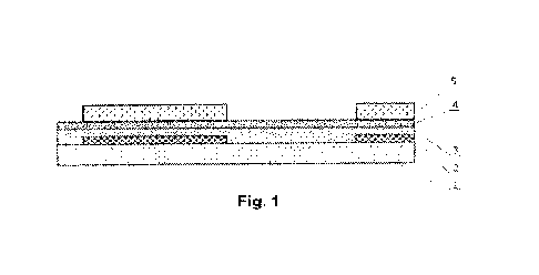
The multilayer surface, the cross-section of which is shown in Fig. 1, in
addition
CA 03236895 2024- 5- 1
WO 2023/085958
PCT/PI,2022/050078
to the visual effect of the imprinted design, also gives a tactile feel. The
applied
27 pm-thick porous structure correlating with the individual elements of the
main
design has a gloss level of 1 '-2' measured in a 60 geometry.
Example 2 ¨ positive mould, asynchronous effect
The decorative layer 2 is applied to the carrier 1 in the form of a plastic
film
band in the same manner as described in Example 1. The printed carrier 1 is
then coated with the protective layer 3, which is Primer FG 2810. This coating
is
carried out using an intaglio cylinder, which applies approx. 5g/m2 of the
primer.
This layer is cured in a dryer at a temperature of 75 C,
Then the structure is coated with the first layer of the topcoat electron
curable
varnish 4 using the 3tvVS coating system. The varnish used at this step has
the
following composition:
FL 27694 - 0.8 part
FLE 27800 - 0.2 part
- FZ 2711 - 0.07 part
- FZ 2720 - 0.15 part
Photoinitiator UZ 7381 ¨ 0.01 part
The obtained coating of the topcoat electron curable varnish layer 4 with a
grammage of 8 g rT12 is exposed to an excimer lamp emitting radiation with a
wavelength of 172 nm, which causes the coating to become matte. Then the
layer 4 is subjected to the pre-polymerization (gelation) process in the
electron
beam generator. The generator parameter settings are as follows:
- Dose 2 kGy
- 100 kV high voltage.
The resulting surface has a gloss level of 7 when measured in a 60 geometry.
The coated band then advances to the intaglio cylinder station with a pattern
that is asynchronous with the individual main decorative elements (decorative
layer 2). At this step, the structural electron curable varnish layer 5 is
applied,
and the varnish has the following composition:
FLE 27800 - 1 part
CA 03236895 2024- 5- 1
WO 2023/085958
PCT/PI,2022/050078
11
- FZ 2720 -0.15 part
- Photoinitiator Omnirad 819¨ 0.005 part
Photoinitiator UZ 7381 ¨ 0.01 part
The structural coating formed by electron curable varnish (5) is stabilized
under
the action of UV rays with a wavelength of 254 nrn using a PAC lamp The
surface is then exposed to an excimer lamp emitting radiation with a
wavelength
of 172 nm. This treatment is followed by the final curing in the electron beam
generator in the area of the entire thickness of all varnish layers. The
generator
parameters are as follows:
- Dose 40 kGy
- 110 kV high voltage.
The multilayer surface, the cross-section of which is shown in Fig. 2, in
addition
to the visual effect of the imprinted design, also gives a tactile feel.
The applied 22 pm-thick asynchronous porous structure, which does not
correlate with the individual elements of the main design, has a gloss level
of
1 -2 measured in a 60' geometry.
Example 3¨ negative mould, synchronous effect
The decorative layer 2 and the protective layer 3 are applied to the carrier
layer
1 as described in Example 1,
The next step is to apply the topcoat electron curable varnish layer 4 in the
3WS
coating system. The varnish used at this step has the following composition:
- FLE 27800 - I part
- FL 2720- 0.15 part
- Photoinitiator UZ 7381 ¨ 0.02 part
The obtained coating of the topcoat electron curable varnish layer 4 with a
gramrnage of 8 g / M2 is exposed to an excimer lamp emitting radiation with a
wavelength of 172 rim, which causes the coating to become matte. Then the
layer 4 is subjected to the pre-polymerization (gelation) process in the
electron
beam generator. The generator settings are as follows:
Dose 2 kGy
CA 032361395 2024- 5- 1
WO 2023/085958
PCT/PI,2022/050078
12
- 100 kV high voltage.
The resulting surface has a gloss level between 10 and 20 when measured in a
60 geometry.
The next step in the production process according to the invention is to apply
the structural electron curable varnish layer 5 , which is synchronous with
each
part of the design, as shown in Fig. 3. A structure is applied whose varnish
has
the following composition:
- FL 27694 - 0.9 part
- FLE 27800 - 0.1 part
- EZ 2711 -0.07 part
- FZ 2720 - 0.15 part
- Photoinitiator Omnirad 2022 ¨ 0.005 part
- Photoinitiator UZ 7381 ¨ 0.01 part
The surface is stabilized under the action of UV rays with a wavelength of 395
am using an LED lamp. The surface is then exposed to an excimer lamp
emitting radiation with a wavelength of 172 nm. This treatment is followed by
the
final curing in the electron beam generator in the entire thickness of all
varnish
layers. The generator parameters are as follows:
- Dose 40 kGy
- 110 kV high voltage.
The multilayer structure, the cross-section of which is shown in Fig. 3, in
addition to the visual effect of the imprinted design, also gives a tactile
feel.
The layer of cured varnish applied with a negative intaglio cylinder has a
thickness of 25 pm, gloss level of 80 measured in a 60 geometry.
Example 4 ¨ off-line varnishing, asynchronous negative mould The
decorative layer 2 and the protective layer 3 are applied to the carrier layer
1 as
described in Example 1.
In the next technological cycle, the topcoat electron curable varnish layer 4
is
applied with the 3WS coating system. The varnish used has the following
CA 03236895 2024- 5- 1
WO 2023/085958
PCT/PI,2022/050078
13
composition:
- FLE 27800 - 1.0 part
FZ 2720 - 0.1 part
- Photoinitiator UZ 7381 ¨ 0.01 part
The obtained coating of the topcoat electron curable varnish layer 4 with a
grammage of 8 g / ill2 is exposed to an exciiner lamp emitting radiation with
a
wavelength of 172 nrn, which causes the coating to become matte. Then the
topcoat electron curable varnish layer 4 is subjected to the pre-
polymerization
(gelation) process in the electron beam generator. The generator settings are
as
follows:
- Dose 3 kGy
- 100 kV high voltage.
The obtained surface has a gloss level between 1 and 20 measured in a 60
geometry.
The semi-finished product prepared in this way is rolled up on a roil and is
ready
for the next processing step.
In the next off-line technological cycle the asynchronous structural electron
curable varnish layer 5 is applied to the individual elements of the wood-like
design at another varnishing machine.
At this step of the process, the varnish has the following composition:
- FL 27692 - 0.9 part
FLE 27800 - 0.1 part
- FZ 2711 -0.07 part
- FZ 2720 - 0.2 part
Photoinitiator Omnirad 2100¨ 0.005 part
Photoinitiator UZ 7381 ¨ 0.01 part
The surface of the structural electron curable varnish layer 5 is stabilized
under
the action of UV rays with a wavelength of 395 nm using an LED lamp. The
surface is then exposed to an excimer lamp emitting radiation with a
wavelength
of 172 nm. This treatment is followed by the final curing in the electron beam
generator in the area of the entire thickness of all varnish layers. The
generator
CA 032361395 2024- 5- 1
WO 2023/085958 PCT/PI,2022/050078
14
parameters are as follows:
- Dose 40 kGy
- 110 kV high voltage.
The layer of cured varnish, the cross-section of which is shown in Fig. 4, in
addition to the visual effect of the imprinted design, also gives a tactile
feel.
The layer of cured varnish applied with a negative intaglio cylinder has a
thickness of 29 pm, gloss level of 6 measured in a 60" geometry,
Example 5 - varnishing without print on the carrier
The protective layer 3 is applied directly to the carrier layer 1, i.e. paper
without
any decorative imprinted design, in the same manner as shown in Example 1.
Then, over the entire band width, the topcoat electron curable varnish layer 4
is
applied using the 3VVS varnishing system. At this step of the process, the
varnish used has the following composition:
- FL 27694 - 0.9 part
FLE 27800 - 0.1 part
- FZ 2711 - 0,07 part
- FZ 2720 -0.15 part
Photoinitiator UZ 7381 ¨ 0.01 part
The obtained topcoat electron curable varnish layer 4 with a grammage of 8 g
M2 is exposed to an excimer lamp emitting radiation with a wavelength of 172
nrn, which causes the coating to become matte. Then the layer 4 is subjected
to
the pre-polymerization (gelation) process in the electron beam generator. The
generator settings are as follows:
- Dose 2 kGy
- 100 kV high voltage.
The obtained surface has a gloss level of 8 measured in a 60' geometry.
The carrier band then advances to the intaglio cylinder station. The second
structural electron curable varnish layer 5 is applied, and the varnish has
the
following composition:
CA 03236895 2024- 5- 1
WO 2023/085958
PCT/PI,2022/050078
FLE 27800 - 1 part
- FZ 2720 - 0.15 pert
Photoinitiator Omnirad TPO-L ¨ 0,005 part
Photoinitiator UZ 7381 ¨ 0,01 part
The surface of the structural electron curable varnish layer 5 is stabilized
under
the action of UV rays with a wavelength of 254 nm using a PAC lamp. The
structure is then exposed to an excimer lamp emitting radiation with a
wavelength of 172 nm. This treatment is followed by the final curing in the
electron beam generator in the area of the entire thickness of all varnish
layers.
The generator parameters are as follows:
- Dose 40 kGy
110 kV high voltage.
The 23 pm-thick rnultilayer "porous" structure, the cross section of which is
shown in Fig. 5, has a tactile feel and a gloss level of - 20 measured in a
800
geometry.
Example 6 - off-line varnishing, positive mould, asynchronous effect, 3
layers of electron curable varnish
The decorative layer 2 and the protective layer 3 are applied to the carrier
layer
1 as described in Example 1.
In the next technological cycle, the first topcoat electron curable varnish
layer 4
is applied with the 3WS coating system. The varnish used has the following
corn position:
- FL 27692 - 0.8 part
- FLE 27800 - 0.2 part
- FZ 2711 - 0.07 part
FZ 2720 - 0.15 part
Photoinitiator UZ 7381 ¨ 0.02 part
The obtained topcoat electron curable varnish layer 4 with a grammage of 8 g /
rn2 is exposed to an excimer lamp emitting radiation with a wavelength of 172
CA 032361395 2024- 5- 1
WO 2023/085958 PCT/PI.2022/050078
16
nrn, which causes the coating to become matte. Then the layer 4 is subjected
to
the pre-polymerization (gelation) process in the electron beam generator. The
generator settings are as follows:
- Dose 2 kGy
- 100 kV high voltage.
The obtained surface has a gloss level of 3 measured in a 60 geometry,
The band then advances to the intaglio cylinder station with a pattern that is
asynchronous with the individual main decorative elements formed in the
decorative layer 2. The structural electron curable varnish layer 6 is
applied,
and the varnish has the following composition:
- FLE 27692 - 0.9 part
- FLE 27800 - 0.1 part
FZ 2720 - 0.15 part
- Photoinitiator UZ 7381 ¨ 0.01 part
The surface is exposed to an excimer lamp emitting radiation with a wavelength
of 172 nm, which causes the surface to become matte. Then the structural
electron curable varnish layer 6 is subjected to the pre-polymerization
(gelation)
process in the electron beam generator. The generator parameter settings are
as follows:
- Dose 3 kGy
- 100 kV high voltage.
After this step, a decorative structure with a thickness of 4 pm and a gloss
level
of 5 is obtained, measured in a 60 geometry.
In the next off-line technological cycle the next structural electron curable
varnish layer EB 5 is applied. The layer is applied with an intaglio cylinder
with a
greater depth of engraving than in the electron curable varnish layer 6
application step. The varnish composition In this part of the process is as
follows:
- FLE 27800 - 1 part
- FZ 2720- 0.15 part
Photainitiator Omnirad 819 0.005 part
CA 03236895 2024- 5- 1
WO 2023/085958 PC T/P
L2022/050078
17
- Photoinitiator UZ 7381 ¨ 0.01 part
Subsequently, the surface is stabilized under the action of UV rays with a
wavelength of 395 nm using an LED lamp. The surface is then exposed to an
excimer lamp emitting radiation with a wavelength of 172 nm. This treatment is
followed by the final curing in the electron beam generator in the area of the
entire thickness of all varnish layers. The generator parameters are as
follows:
- Dose 40 kGy
- 110 kV high voltage.
The obtained surface, the cross-section of which is shown in Fig. 6, in
addition
to the visual effect of the imprinted design, also gives a tactile feel. The
total
thickness of the structural electron curable varnish layer 5 is 30 pm, and the
surface has a gloss level of 1 - 2 measured in a 60 geometry.
In all variants of the invention presented in the above examples, the varnish
mixture in both application units contains a special additive improving the
bond
strength between the individual layers. The additional condition for achieving
good bond strength is that each layer of varnish is subjected to pre-
polymerization (gelation) at the stage of producing a matte surface preceding
the last layer.
CA 03236895 2024- 5- 1