Note : Les descriptions sont présentées dans la langue officielle dans laquelle elles ont été soumises.
20365-2636
SPECIFICATION
"METHOD AND CIRCUIT ARRANGEMENT FOR THE TRANSMISSION
OF DATA SIGNALS BETWEEN TWO CONTROL DEVICES BELONGING
TO A LOOP SYSTEM"
and we do hereby declare ~hat the following is a true, clear and
exact description of same.
BACKGROVND OF_THE I~VENTION
Field of the Invention
-
~e invention relates to a method and to a circuit
arrangement for the transmission of data signals between cont:rol
devices connected to one another via a clock-controlled loop
system opera-ted directionally dependent.
Description of the Prior Art-
Dat~ transmission systems are known wherein the control
devices are control devices of a data switching system, whereby
data signals to be output proceeding from a control de~ice to a
further control device are transmitted in sections ~rom control
device to control device in the form of a signal block together
with a receiver address identifying a control device as -the
receiver which precedes the data signals. ~he signal block is
characteri~ed by a block start identifier, a sender address
~6~3~
20365-2636
ident;fying the control device emitting the signal block as the
transmitter which is attached to the data signals, ancl by a block
end identifier. In response to -the acceptance of a s:ignal hlock,
a control device selec-ted as the recelver emits an acknow]edyement
signal together with -the sender address for that control device
from which the received signal block had been previously emitted~
A method is known wherein a signal block constructed as
described above is transmitted proceeding from one control device
of a loop system -to a further control device in German OS 31 36
495. In the control device selected as the receiver, an acknow-
ledgement informatlon signal block is compiled in response to the
reception of a signal block, this acknowledgement in-formation
signal block being subsequently transmitted to that control device
from which the signal block just received had been previously
emitted. The ackncwledgement in-formation signal blocX is thereby
compiled in the same way as the previously received signal block,
i.eO, receiver address and sender address for the ac1snowledgement
signal to be transmitted are attached to the actual acknowledge-
ment signal. The two addresses for this purpose are derived from
the signal block just receivedO A control outlay whlch is some-
times undesired is thus required in the indlvidual control devices
for the reception of signal blocks and the transmission of
acknowledqement information signal blocks connected therewith
SUMMARY OF THE INVENTION
An object of the presen-t invention is to provide a
method and circuit arrangement o the type described above,
, ....
. . .
3~
20365-2~36
wherein signal hlo~ks and acknowledgement slgnals can be trans-
mitted between two control devices connected to the loop system
with a low control circuitry outlay~
In accordance with the principles oE the present
invention, the above objec-t is achieved in a method and system
where1n, in response to the appearance of a signal block having a
b~ock start iden-tiEier and a receiver address, the signal block
is copied in the receiving control device identified by the
receiver address for possible processing. The receiving control
device then cancels the block start identiier of the signal
block, and attaches an acknowledgement signal to the sender
address identified by the block end identifier. This modified
signal block is then returned to the loop system and is trans-
mitted around the loop back to the sending control device. The
acknowledgement signal is recognized by the control device
identified by the sender address, such recognition occurring due
to the appearance of the block end identifier and the sender
address. The sending control device then accepts the mod;fied
block signal for evaluation.
The method and apparatus disclosed herein have the
advantage that the received signal block is directly employed ~or
generating an acknowledgement signal intended for the sending
control device. The block start identifier originall~ belonging
to the signal block is cancelled, and an acXnowledgement signal
Eor the receiving control device is simply attached to the sender
address already identified by the block end identif-ier. By
cancelling the block start iden-tifier, the forwarded .signal blocX
-- 3 --
3~ ~
20365-2~36
is no longer identified by other control devices as such. The
sender address tran~mitted in conjunction with the block end
identifier, however, is still recognizable~ An acknowledgement
signal confirming reception of the signal block is attached there-
to by the receiving control device. The con-trol device from which
the signal block was originally sent, need only recognize the
appearance of the sender address in combination with the block end
identifier in order -to accept the acknowledgement signal intended
for that control device.
- 3a -
~2~
20365-2636
In one embocllment of the invention, the circuit includes
a reception controller and a receiver having a reception memory
for accepting signal blocks, and also lnc:Ludes an acknowledgement
signal receiver. By separating the receiver arrangement into a
reception memory and an acknowledgement signal receiver, it is
possible to accept signal blocks and acknowledgement signals in
the control device with a low circuit outlay, and to process these
signals in components following -the receiver arrangement. The
reception memory may be, for example, a write/read memory
controllable by two separate means for executing write/read
events. By this expedient, the working speed of the control
device can be adapted to the transmission rate of the loop system.
For this purpose, it is preferable that the write~read memory be
addressed in circulating Eashion by counter arrangements. Given
circulating addressing of the write/read memory, to avoid
overwriting signal blocks already stored in the write/read memory
but not yet read out, a counter arrangement may be provided which
monitors the filling status of the write/read memory and, when a
prescribed filling state is reached, aborts acceptance of the
just-received signal bLock by inhibiting the counter which
executes the write-in eventsO
In accordance with a broad aspect of the invention there
is provided a method for transmitting data between two control
devices in a system having a plurality o~ control devices
connected by at least one clock controlled trans~ission loop
operated directionally dependent, said method comprising the steps
o~: generating a signal block in a sending control device ~or
20365-263
transmission to another o:E said plurality of control devi.ces
intended as a recelving control dev.ice; generati.ng a ~Ei:rst ent:ry
preceding said data signals in said sending contKol device having
a receiver address identi-Eying said intended receiving contro].
devi.ce; generating a last entry following said da~a signal in said
sendi.ng control device having a sender address identiEying the
sending control device and a block end identiEier; emittiny said
Eirst entry, said data signals/ and said last entry as a signal
block to said loop for transmission around said loop to all other
control devices; a control device having an address corresponding
to said receiver address, in response to the appearance of the
block start identifier and said receiver address in said signal
blockr copying said signal block therein for possible processing
by said receiving control device; cancelling said block start
identifier from said block signal in said receiving control
device; attaching an acknowledgement siynal -to said sender address
identified by the block end idantiEier in said receiving control
device; re-emitting said signal block with the acknowledgement
signal and the block start identifier cancelled to said loop
system; inhibiting copying of a signal block not having a block
start identiEier in all contro:l devices; and said sending control
device, upon recognition of its sender address in combination with
said block end identiEier, accepting said acknowledgement signal
or interpretation.
In accordance with another broad aspect of the invention
there is provided a ~ata transmission system having a plurality of
control devices connec~ed by at least one clock-controlled
4a
~2~
20365--2636
transmlssion loop ope:rated directional depend0nt~ each control
device inclucling: tneans Eor generating data signals -Eor
transmission to another control device around said loop :Erom said
control device to control device; means ~or generating a first
entry preceding said data signals having a receiver address
identiEying anothe:r control device in said plurality of control
devices intended to receive said data signals and a block start
identifier ; means Eor generatiny a last entry following said data
signals identifying the control device emitting said data signals
and a block end identifier; means for emitting said first entry,
said data signals, and said last entry as a signal block to said
loop for transmission around said loop to all other control
devices; means/ upon receipt oE said signal block, if the
receiving control device is the control device identified by said
receiver address, for copying said signa:l block for possible
processing by the receiving control device; means in the receiving
control device for cancelling the block star~ identifier of said
signal block; means in the receiving control device for attaching
an acknowledgement signal to said sender address; means for re-
emitting said signal bloclc with the acknowledgement signalattached thereto and the block start identifier cancelled to said
transmission loop for transmission around said loop; means i~ all
control devices for inhibiting copying of a signal block not
having a block start i.dentifier; and means Eor accepting said
acknowledgement signal in the control device which originally
transmitted said signal block upon recognition of said sender
address in combination with said block end identifier for
4b
20365-2636
lnterpreting said acknowledgement signal~
The invention shall be set forth in greater detail below
by way of example with :reference to drawings.
FIGo 1 shows a block circuit diagram of a data switching
system formed of a loop system wherein the invention is applied,
FIG~ 2 shows a block circuit diagram of portions of the
structure of one of the interface circuits schematically shown in
FIG~ 1 and of the structure oE a switching unit or line
termination unit connec-ted thereto.
FIG~ 3 shows the structure o:E a receive buffer arrange-
4c
20365-2~36
ment present in the interface cireuit of F'IG. 2.
FI~. 4 s~ows the s-tructure o:E a reception controller
pertaining to the reeeive buffer arrangement oE .FIG. 3.
FIG. 5a through 5d show the skructure of signal blocks
which are transmit-ted via the loop systern.
DESCRIPTION OF THE PREFERRED EMBODIMENTS
-
FIG. 1 shows a data switching system including a
plurality of switehing units SUo through SUn. Based on the l.oad
division principle, these switehing units execute the switching
funetions requirecl Eor the transmission of data signals. For this
purpose, t~e switching units are eonneeted in common to a loop
system. Sueh a loop system ean be eomposed of a single, el.osed
ring conduetor arrangement. Such a loop system, however, as shown
in FIGURE 1 by way of example, can also be eonstructed o~ two
mutually independent ring eonduetor arrangements RINGO and RIN~l
whieh proeeed in parallel~ For example, given outage of one of
the ring eonduetor arrangements, sueh a redundaney makes it
possible to exeeu-te the transmission of signal bloeks and aeknow-
ledgement signals on the respeetively other ring eoncluetor
arrangement.
'Fhe eonneetion of the said switching units SUo through
~Un to the two ring eoncluetor arrangements respeetively ensues
via a separate interface eireuit RA ~or eaeh oE the ring eondue-
tor arrangements, this interfaee eireuit RA to be discussed in
greater cletail below.
Line termination units TUo through ~Uk are also eon-
neeted to the saicl ring eonduetor arrangements RINGO and RINGl,
20365-2636
being also respec-tively connected thereto via a separate interface
circuit RA for each of the ring conductor arranyements toget-'ner
with the associated interface circuits, the~e line termination
units serve for the data siynal transmission between the said
switchi.ng units and transmission lines connected to subscriber
equipment, the transmission lines being connected to the :Line
termination units TUo throuyh TUk. Each of the line termination
units has a plurality of line terminations LTo through LTm for
such a connection of transmission lines~
The circuit units formed of the swi-tching units or the
line termination units and the associated interface circuits are
also referred to below as control devicesO If the loop system is
composed of only a single ring conductor arrangement, only a
single interface circuit belongs to a control unitO
Within the switching system shown in Fig. 1, i.e.,
between the switching units and the line termination units, the
transmission of data signals ensues in the form of signal blocks
which, as data slgnals in the course of the set-up of a connec-
tion, respectively comprise signaling infor~ation and, given an
established connection, comprise the message si.gnals to be trasls
mitted between the subscriber equipment coming into consi-
deration. In addition to the actuaL data signals which are
respectively formed of a plurality of bits, for example 8 bits,
each siynal block to be transmitted cosltains a receiver address
identifying at least one of the control devices as the receiver, a
start identifier indicating the beginning of a signal block, as
end idesltifier indicating the end of a signal block, a sender
6 ~3~t~
20365-~636
address identifying the control device emitting t'he signal block
as -the sender, and at leas-t one ~cknowledgement sign.~l or blank
acknowledgement. A siynal block constructed in such fashion,
which shall be se-t Eorth in yet greater detail below, can thereby
be emit-ted to one of the ring conductor arrangements only when the
sending control device has previously received a transmit authori-
zation signal transmitted from control device to control device
which respectively dri~es the control devices into a transmit
authorization status.
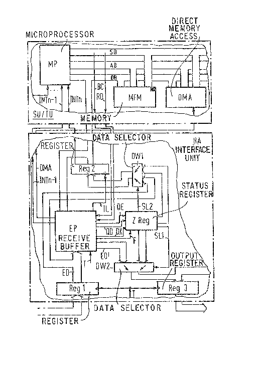
Fig. ~ shows the structure of a control device in
greater detail. As mentioned ahove, such a control device is
either compo~ed of a switching unit or a line termination unit,
indicated in Fig. ~ by the reference SU/TU, and of a plurality of
interface circuits RA corresponding in number to the plurality of
ring conductor arrangements. Only one of these interface circuits
is shown in Fig. 2 since all interface circuits connected to the
switching units or to the line termination units internally
comprise the same structure~
I'he unit (switching unit or line termination unit)
referenced SU/TU and shown in Fig. 2 includes a microproces~or
arrangennent which controls both transmit as well as receive
events. O~ this microprocessor arrangement, a microprocessor MP,
a memory arrangement MEM comprising read-only memories ~program
nnemories) and write/read memories and a means for a direct memory
access DMA are ~hown. The rnemory arrangement MEM and t'he direct
memory access DMA are in communication with t'he microprocessor MP
via a bus system~ The bus system includes a data bus DBt an
20365-2636
address b~s AB, and a control bus SB. The inter:Eace circuit RA :is
also in communication with the ~icroprocessor MP via the data bus
~B and via the lines o-f -the contro]. bus referenced RD and BC.
Further, two control lines referenced INTn-l and INTn of -the
interface circuit lead to interrupt inputs INTn-l and INTn of the
microprocessor MP. The interface circu:it RA is aLso connected -to
-the means for a direct memory access DMA, via a further line
referenced DMA.
An interface circuit RA includes devices Eor handling
received signal blocks and acknowledgement signals as well as
devices for the emission oE signal blocks pending in the control
deviceO In Eig. 2, only those devices for handling received
signal blocks and acknowledgement signals which relate to the
present invention are shown.
At the interace to the appertaining ring conductor
arrangement which, -for example, can be assumed -to be the ring
conductor arrangement RING0, the interface circuit RA shown in
Fig. 2 has a receive register Regl which is supplied with signals
transmitted via the ri.ng conduc-tor arrangement in parallel :Eorm.
For this purpose, this register Regl is controlled from a clock
generator which supplies clock signals corresponding to the
transmission rate of the ring conductor arrangement to an input of
-the input register Regl via a line 1'. At its ou-tput side, this
input register Regl is connected to a receive buffer arrangement
EP via a line arrangement ED and to first inputs o a data
selector DWl~ As shall be set forth below, the receive buffer
arrangement EP thereby serves for the acceptance of signal blocks
-- 8 --
20365-2636
and acknowledgement. signals as well as for forwarding these to the
control device followiny in the loop system.
rFhe recei~e buffer arrangement EP i5 in com~unication
with the unit SU/TU via the data bus DB, t.he aforementioned :lines
RD and BC of the control bus SB, and via the lines DMA and INTn-
1. The receive buffer arrangemen~ is supplied with clock signals
via the aEorementioned line T and itself emits control signals to
a status register ZReg via lines QE, QD, QK and F and ~o a clock
input of a register Reg2 serving as acknowledgement recei.ver via
a line TL. The receive buffer arrangement EP is also in communi-
cation with first inputs of a further data selector DW2 via a line
arrangement ED'.
Second inputs of the data selector DW2 and of the data
selector DWl are connected to outputs of the status register ZReg.
Both data selector~ are thereby controlled by the status register
via the lines SLl and SL2. At its output side, the data selector
DWl is connected to signal inputs of the reyister Reg2, whicn has
its signal outputs connected to the data bus DB. By contrast, the
output side of the data selector DW2 is connected to signal
inputs of an output register Reg3. This register Reg3 is supplied
with clock signals via the line T and emita signals supplied from
the data selector DW2 at its signal outputs onto the riny
conductor arrangement connected to the interface circuit RAo
Moreover, the signal inputs of the output register Reg3 are also
in communication with devices for the emission of signal blocks
ready in the control device. Elowever, as already set forth, the
6 ~
2~365-2~36
structure of these devices shall not be discussed in greater
detail.
The interaction oE the circuit parts shown in Fig. 2 in
the acceptance and for~arding of signal blocks and acknowledge-
ment signals will be set forth before the structure of the
receive buffer arrangement EP is discussed in greater detail~
Within the loop system, data signals can be optionally
transmitted to a single control device selected as receiver or to
a group of control devices. It shall be assumed first that data
signals from a control device of the loop system are only to be
transmitted to a single control device. For this transmission,
the control device from which the data signals are to be emitted
compiles the data signals in the unit SU/TU to form a signal
block. Such a signal blocX is schematically shown in Fig. 5a. It
is introduced by a receiver address EADR identifying the control
device selected as the receiver. This receiver address i9
followed by the data signals DSl through DSn to be transmitted. A
sender address SADR identifying the control device sending this
signal block is attached to these data signals. Finally, the
signal block is terminated by a blank acknowledgement LQ prepared
by the sender. Among other things, two identifier bits are
respectively attached to the signals of a signal block. A first
identifier bit (column A in Figs. Sa through 5b) serves for
identifying the start o a signal block. In a corresponding way~
a second identifier bit (co]umn E) ~erves for the identifica-tion
of the end of a signal block. The start and the end of a signal
- 10 -
20365-2636
block may be indicated, -Eor example, by the logic status "1" of
the respective identifier bit. The logic st.atus "1" of the iden-
tifier hit A shall be referred to below as the block start identi-
fier and the logic status "1" of the iden-tified bit E shal1. be
referred to as the block end identifier. As shown in Fi.gO 5a, the
block start identiEier is transmitted together with the receiver
address as a first entry and the block end identifier is
transmitted together with the sender address as a last entry.
Upon arrival of a tra~smit authorization signal trans-
mitted from control device to con-trol device and respectlvel.y
successively driving the control devices into a transmit authori-
zation status, a signal block compiled in the way just described
is subsequently emitted by the unit SU/TU (Fig. 2) to the ring
conductor arrangement connected to the interface circuit RA, via
the output register Reg3. Every one of the interface circuits
connected to the ring conductor arrangement accepts the signals
bel.onging to the transmitted signal block via its input register
Regl. With the assistance of the receive buffer arrangement EP
belonging to the respective control device, a comparison of the
receiver address transmitted in the signal block together with the
block start identifier to the address assigned to the respective
control device within the loop system is first execuked~ If the
comparison does not yield a coincidence of the addresses compared
to one another, the receive bufEer arrangement ~P forwards the
received signal block via the line arrangement ED' tG the data
selector DW2 unmodified. Via the data selection DW2 and the out-
203~5-2636
put register Reg3, the signal block then again arrives onto the
ring conductor arrangement.
If, however, the address co~parison yields a coincidence
of -the addresses compared to one another, the signal block just
received is copied in the receive buffer arrangement ~P. The
block start identifier is cancelled, and the signal block itself
is forwarded via the line arrangement ED' to the control device
following in the loop system. Given this forwarding, the status
register ZReg attaches another acknowledgement signal EADR, QS to
the sender address SADR, so that the blank acknowledgem~nt (LQ~
originally contained in the signal block is overwritten. For this
attachment, the status register ZReg is supplied with a control
signal via the line QE, from the receive buffer arrangement EP
which monitors the appearance of the block end identifier E and of
the sender address SADR. The forwarded signal block is shown in
Fig. 5b.
After the copying of a signal block, the receive buffer
arrangement EP emi-ts a control signal indicat-lrlg the readiness of
a received signal block, via the line DMA' to the means for a
direct memory access DMA. The direct memory access DMA then
effects transfer of the signal block into the unit SU/TU. The
microprocessor MP is informed of the end of the signal block by an
interrupt signal at its interrupt input INTn 1, from the receive
buffer arrangement EP.
Since the block start identifier A originally transmit-
ted in the signal block is erased in the forwarding thereof, the
signal block i.s no longer perceived as such, so that it cannot be
- 12
20365-2636
accepted by following control devices. Only the sender address
SADR transmitted together with the block end identifier R can
still'be percelved as such. The appearance of bLock end identi-
fier and sender address is moni-tored in the control device Erom
which the just-acknowledged signal block had been previous:Ly emit-
ted, namely in the receive buffer arrangement EP. When the buffer
arrangement EP recognizes the appearance of a block end identifier
and sender address, it emits a control signal ~o the acknowledge-
ment register Reg2 via the line TL, this acknowledgement register
Reg2 subsequently accepting the acknowledgement signal QS
transmitted following the sender address, from the line arrange-
ment ED via the data selector DWl. In response to the acceptance
of such an acknowledgement signal, the acknowledgement register
Reg2 emits an interrupt signal to the microprocessor Mp via the
line INTn. On the basis of this signal, this then accep-ts -the
acknowledgement signal ready in the acknowledgement register -for
an interpretation. The transmit event is thus ended.
The case wherein a signal bloclc is to be transmitted to
a group of control devices shall now also 'be considered. For
thisr too, a signal block is first compiled in the control device
emitting the signal block, in the format shown in Fig. 5a and is
emitted to the ring conductor arrangement. One difEerence is that
a group of control devices is now identified by the receiver
address EADR. A group can optionally comprise all control devices
belonging to the ring conductor arrangement or can comprise only a
part of these control devices.
- 13 -
2036~-2636
With the emission o-f the signal b:Lock to the ring con-
ductor arrangement, the mi.croprocessor MP o:E the emi-t-tiny control
device also emi.ts a multi--address signa:1 BC to the receive buffer
arrangement EP via the line also referenced BC. This multi-
address signal indicates that a signal block has been emitted to a
group of control devices.
The transmission of the signal block again ensues from
control device to control device in the way described above.
Control devices not identified by the receiver address forward the
received signal block unmodiied. The first control device
belonging to the group identified by the receiver addresst by
contrast, copies the received signal block in its receive buffer
arrangement EP. Without the previous blocX end identifier E, the
signal block is forwarded to the control device following in the
ring conductor arrangement. In t'nis forwarding and in response
to a data control signal emitted by the receive buffer
arrangement, this control signal being transmitted via the line
QK, the status register ZReg attaches another acknowledgement
information seyment to the sender address SADR together with a
block end identifier a.s a new last entry. The acknowledgement
information segment is composed of the address EADRl assigned to
the receiving control device withi.n the ring conductor arrangement
and o~ the actual acknowledgement signal QSl relating to the
recepti.on of the sig.naL blockO The signal block emitted by the
first control device belonying to the g:rollp is shown in Fig. 5c.
For the above attachment of the acknowledgement information
segment and of t.he block end identifier the da-ta selector DW2
- 14 -
3 ~3
2~365-263
shown in Fig. 2 i9 appropriately driven via the llne SI.l
proceeding from the status regis-ter ZReg.
The received signal block is also copied in the further
control devices belonging to the group and, without the pre~ious
block end identiEier, is forwarded to the control de~ice following
in the loop system. An aeknowledgement in~ormation segment and a
block end iden-tifier are again respectively attached to the last
acknowledgement information transmitted in the signal block. The
signal block emitted by the mth eontrol device belonging -to
the group is shown in Fig. 5d. The signal block which the last
eontrol deviee belonging to the group emits includes acknowledge-
ment information for all control deviees belonging to the groupO
The signal block containing the acknowledgement signals
of all control deviees belonging to the group is accepted into
that eontrol deviee from which the original signal block was
emitted. ~his aceeptanee can again ensue in the form of a copying
event in the reeeive buffer arrangement ~P of t.hat control device;
to whieh a multi-address signal BC had heen supplied with the
original emission of the signal bloek. The copying event is ini-
tiated in response to the appearance of the bloek start identifiertogether with the ~ulti-address signal. The signal block itself
is again emitted to the ring eonduetor arrangement with eaneellat-
ion of both the bloek start identifier and the bloek end identi-
fier, via the output register Reg3. Sinee both identifiers have
now been eaneellecl, the forwarcled signal block can no longer be
reeognized by the eontrol deviees fol1.owing in -the ring conductor
arrangement.
- 1.5 -~
lZ~6~3~D
20365~-2636
After copying the signal bLock including the acknow-
ledgement information, i.e~, upon appearance oE the block end
identifier belonging to this signal block, the r~cei~a buffer
arrangement EP emits a control. signal to the status register ZReg
via the line QD. In response there-to, this status regis-ter ZRey
offers an acknowledgemen-t signal relating to the reception of this
signal block, this acknowledgement signal being transferred via
the data selector DWl into the acknowledgement register Reg2 For
this transfer, the acknowledgement register is supplied with a
corresponding control signal from the receive buffer arrangement
via the line TL. Moreover, the data selector DWl is appropriately
controlled for this acceptance by the s-tatus register ZReg via the
line SL2.
Transfer of the acknowledgement signal trans~itted into
the acknowledgement register Reg2 and of the signal block situated
in the receive buffer arrangement EP into the unit SU/TU again
ensues in the way already set forth above. After this transfer,
an evaluation of all accepted acknowledgement signals ensues in
the unit SU/TU. Moreover, the transmit authorization signal
received by the control device is forwarded to the control device
following in the ring conductor arrangement.
With reference to Fig. 3 and 4, the structure of the
receive buffer arrangement referenced EP in Fig. 2 shall now be
discussed in greater detail below. As shown in Fig. 3, the
receive buffer arrangement contains a write/read memory R~M having
a plural.ity of memory celLs for the acceptance of signal blocks
including the block end identifiers~ For the acceptance of signal
- 16 -
~6~
203~-2536
blocks, t~is memory has its data signal inputs/outputs connected
to the line arrangemen-t ED already shown i.n Fig. 2 and for an
emission of signal blocks, 'has its data signal inputs/outputs
connected via a register Reg4 to -the data bus DB a'Lso al:ready
presented in Fig. 2. E'or the emission of a signal block, the
register Reg4 is supplied with read-out clock signals via the line
RD belonging to the control bus SB. These read-out clock signals
correspond to the working speed of the respective control device.
For the acceptance of signal blocks, the write/read
memory RAM, by contrast, is suppl.ied with write-in clock signals
at an input WR. These write-in clock signals appear on the line T
and are emitted to the said input of the memory via an AND element
Gl. This AND element is driven into its conducting state by a
control signal appearing on a line ANF. rFhis control signal is
emitted fxom a reception controller EPS.
rFhe write/read me~nory has its address inputs connected
to a counter LZ via a data selector DW3 and to a coun-ter SZ. The
counter SZ serving as write counter has its clock input connected
to the output of the aforementioned AND element Gl, i.e., it is
supplied with the write clock ~ignals simultaneously with the
write/read memory RAM. Given acceptance of a signal block, the
counter 5Z emits i-ts coun-ter readings, wh;.ch change based on the
measure oE these write-in clock signals at counter ou-tputs for the
write/read memory as address signals. r~nese coun-ter outputs are
in communication with a register Reg5 which is suppli.ed with a
transfer cloc'k pulse vi.a an ~ND element G2. At its input side,
this AND element is connected to the line T and to a line AK
- 17 -
~ 20365-2636
connected to the reception contro]ler EPS. At its output side,
the register Reg5 i8 in commun-;.cation with setting lnput of the
counter SZ. These setting inputs are enabled by a set-ting signa:L
output from the receptlon controller EPS whlch appears on a Line
F. The counter LZ serves as read counter. Its clock input is
supplied with the read-out clock signals app0aring on the line
and it emits its counter readings, which change based on -the
measure of these read-out clock signals to the write/read memory
RAM as address signals when a signal block i5 read out.
The data selector DW3 connected to the two coun-ters LZ
and SZ has its control input also connected to -the line A~F.
~ le receive buffer arrangement EP includes a further
counter IZ. This coun-ter is a bidirectional counter which, for
counting in one direction, is supplied wlth write-in clock signals
from the output of the AND element Gl and, Eor counting in the
other direction, is supplied with read-out clock signals appearing
on the line RDo At its output side, the counter IZ is connected
to inputs of a decoder DEC which, given a defined coun-ter reading
of the counter IZ, emits a status signal to the r0ception contro]
ler EPS via a line SUE.
At its output side, the counter IZ i.s also connected to
a register Reg6 and to an OR element G3. A clock input of the
register Reg6 is supplied with a tran~,fer clock pulse from the A~D
element G2. At its outpu-t side, this register RegG is connected
to setting inputs oE the counter IZ, which a:re again enabled by a
setting signal appearing on the line F.
18 -
~6~V~
~0365-2~36
The output of the a~orementioned OR element G3 is con-
nected to Eirst inpu-ts of an OR element G4. A further input of
this OR element G4 is connected to the negating output of a trig-
ger circuit FF. I~e output of the OR element G4 is connected to
the line DMA. The non~negating output of the trigger circuit FF
is connected to the line INTn-l. The clock input o this trigger
circuit FF is supplied with read~out clock signals appearing on
the line RD. The data input of the trigger circuits FF is con-
nected to the line EK of the data bus DB, whic'n carries the block
end identifierO
The reception controller EPS is in communication with a
plurality of the lines indicated in Fig. 2. At the input side,
these are the line arrangement ED as well as the lines BC and To
At t'he output side, there is a connection to the line arrangement
ED' and to the lines TL, QE, QD, QK and F.
I~e following control events occur in sequence in the
receive buffer arrangement EP shown in E'ig. 3. Upon the appear-
ance of a block start identifier together with a receiver addre~s
iden-tifying the control device, the reception controller EPS emits
a control signal via the line A~F. On the basis oE the control
signal, the write/read memory RAM as well as the two counters SZ
and I2 are supplied with write-in pulses for the acceptance of a
received ~ignal block, via the A'ND elemen-t Gl. Both counters w:ill
be first situated at a basic counter reading whic'h, for example,
can be assumed to be the counter reading '10ll. The counter reading
is then modified with every write-in clock pulse, whereby the
memory cells oE the write/read memory RAM are continuously addres-
-- 19 --
20365-2636
sed with the changing, momentary counter .readlng oE the counter
SZ, and the momentary coun-ter reading of the counter IZ cor.re-
sponds to the momen-tary Eilling state oE ~he write/read memory.
Acceptance of signals belonging -to a signal bLock then ensues
until, with the appearance of the block end identl-Eier belonging
to the signal. block, a control signal inhibi-ting the AND element
Gl is supplied via the line AND from the reception controller EPS,
so that the further emission of write-in clock pulses is pre-
vented. The momentary coun-ter reading just emitted by the two
counters SZ and IZ at this point in time is retained.
As was already set forth in conjunction with Fig. 2, the
unit SU/TU is informed of the presence of a received signal block
by a control signal transmitted via the line DMA. By supplying
read-out clock signals via the line RD and continuous addressing
of the memory cel].s of the write/read memory proceeding ~rom the
counter I.2, the signal block located in the write/read memory is
subsequently transferred into the unit SU/TU by a direct memory
access via the register Reg4 until the appearance of the blo~k end
identifier contained in the signal block just read out. This
block end identifier appears on the line EKl of the data bus DB.
This appearance transfers the trigger circuit FF to its active
condition in which it signals the end of a signal hlock to t'ne
microprocessor via the line INTn-l. In response theretol the
microprocessor interrupts the supply of further read-out clocks.
The trigger circuit FF interrupts the control signal for a direct
memory access transmitted via the line DMA.
- 2~ -
.
~ 20~65-2636
The counter L,Z will also initially begin to count pro--
ceeding fro~ a prescribed basic counter reading, which can be
assumed to be the counter reading "O". The momentary counter
reading just emit-ted by the counter LZ given appearance of the
block end identifier is then retained until the initiatlon of a
further read-out eventO
When reading a siynal block out of the wri-te/read memory
RAM, the read-out clock signals are also supplied to -the counter
IZ. These read-out clock signals effect a counting in the reverse
direction/ so that the momentary counter reading of this counter
is reduced with every read-out clock pulseO The momentary counter
reading thus corresponds to the number of signals of the signal
block which have not yet been read out of the write/read memory
RAM. When the counter reading "O" which indicates the empty
condition of the write/read memory is reached, the OR element G4
is inhibited so that the controL signal transmitted via the line
DMA is interrupted. When -Eurther signal blocks are now received,
t`he control events already set forth occur in sequence. The only
difference is that the counters SZ, LZ and IZ now con-tlnue to
count from the counter readings still pending. In other words,
the initial counter readings of these counters now correspond to
the counter readings most recently reached upon acceptance or upon
read-out of signal blocksl instead of the prescr;bed readings
assumed earlier. The renewed write-in o~ signal blocks into the
write/read memory RAM can already ensue at a point in time at
which previously received signal blocks were not yet capable of
being completely transferred into the unit 5U/TU~ In thi~ case,
- 21 ~
20365-2636
the acceptance vf a signal block just received has p:rio:rlty over
the read-out oE previously received siynal b:locks. In the accep-
tance of signal blocks the counter IZ changes i~s counter reading
in accord with the number o:E memory cells of the write/read memory
R~M which are occu~ied by siynals of the signal blocks and which
have not yet been read out.
Upon reception of a signal. block and in response -to the
appearance of ~he block start identifier transmitted -therewi~h, a
transfer clock pulse is smitted via the AND element G2 -to the two
registers Reg5 and Reg6, due to a signal transmitted via the line
AK. In response thereto, -these registers respectively accept the
momentary counter reading e~itted by the counter respectively
connected there-to as an initial counter reading for a Eurther
acceptance of ~ignal blocks.
When, due to the acceptance of signal blocks into the
write/read memory R~M and a -transfer into the unit SU/TU which has
not yet ensued, a prescribed counter reading which indicates -the
maximum filling state of the write/read memory RAM is reached,
then a status signal to the reception controller EPS i5 e~itted
proceeding from the decoder DEC, this reception controller EPS
subsequently transmitting a set-ting signal via the line F for
enabling the setting inputs of the counters SZ and IZ. The
initi.al counter readings trans~erred into -the registers Reg5 and
Reg6 at the beginning of the signal block just received are thus
transferred i.nto the counters SZ and IZ, i.e., the ~emory cells of
the write/read memory RAM which have already been occupied by
signals of the signal block which cannot be completely accepted
- 22 -
~2~"3~
20365-~636
are again released. Acceptance o-f t~e signal block just received
into the write/read memory R~M is ended. This ensues hy inhibi-
ting the AND element Gl by a control signa1 transmitted vla the
line ANF. The incornple-te acceptallce oE a signal block is also
signaled to the status regis-ter ZReg via the line F shown in
Fig. 2. The status register ZReg subsequently attaches a
corresponding acknowledgement signal to the sender address -trans-
mitted with the signal block just receivedO
Fig. 4 shows -the structure of the reception controller
EPS. This contains two comparator arrangements Vgll and Vgl2 for
comparison of the receiver address transmitted together with the
block start identifier or of the sender address transmitted
together with an acknowledgement signal, to an address assigned
to the appertaining control device within the ring conductor
arrangement~ The comparator arrangement Vgll thereby serves for
an address comparison given reception of a signal block intended
for only one of the control devices and given reception of an
acknowledgement signal~ The comparator arrangement Vgl2 serves
for an address comparison given reception of a signal block
intended for a group of control devices. The comparison address
to be consulted for the respective comparison is supplied by an
arrangement Sl or S2 each shown as a switch arrangement which is
connected to the respective comparator arrangement Vgll or Vgl2.
These arrangements can thereby be arhitrary storage devices. The
comparator arrangement -to be respectively ernployed for an address
comparison is controlled by a signal on the line GA~ This signal
- 23
20365-2636
is a component pa~t of the recei.ver address indicatiny a group of
control clevices ancl identifies this as such.
The outputs oE the two comparator arrangements Vgl:L and
Vgl2 are connected via an OR element G5 to one oE the address
inputs of a read-only memory PROM. Further address inputs o:~ thi~
memory are in communication with a line AK carrying ~he block
start identifier, with a line EK2 carrying the block end identi-
fier, with the lines SUE, BC and with the output of the comparator
arrangement Vgl2. The two ]ines AK and EK2 belong to -the line
arrangement ED.
The read-only memory PROM includes a plurality of
storage locations in which all control signals for handling the
received signal blocks and acknowledgement signals are storedO
This read-only memory PROM has its data outputs connected to a
register Reg7. Via data outputs, this register is in communica-
tion with the lines ANF, QE, QD, QK, TL and F already shown in
FigO 2~ A data output is also additionally connected to a first
control input of a register Reg8. One clock input of the register
Reg7 is also connected to the line T.
A second control input of the register Reg8 i5 connected
to the line BC already shown in Fig. 2. At its input side, this
register is in communication with the line arrangement ED and, at
its output side, is in communication with the line arrangement
ED'.
Dependent on the signals which are supplied at the
moment to the read-only memory PROM at its address inputs, it
e~its a control signal corresponding to these signals which is
- 24 -
3~q3
20365-2636
accepted by the reyister Reg7 and is forwarded to t'he llne comlny
into consideration. The ef~ect of -tl~e control signals appearing
on the lines ANF, QE, QD, QK, I'L and F 'has already been set fort'h
with reference to FigO 2.
Via the register Reg8, each of the signa:L b:Locks
received by the control device is forwarded to the control device
following in -the ring conductor arrangement. In this forwarding a
modification of the signal block may ensue with respect to the
block start iden-tifier and block end identifier contained thereinO
As already set -forth above, the possible modi-fication is, depen-
dent on the type of signal block now to be forwarded, cancellation
of the block start identifier, of the block end identifer or of
both identif;ers.
Although modifications and changes may be suggested by
those sXilled in the art it is the intention oE -the inventor to
embody within the patent warranted hereon all changes and modifi-
catiorls as reasonably and properly come within the scope of their
contribution to the art.
- ~5 -