Note : Les descriptions sont présentées dans la langue officielle dans laquelle elles ont été soumises.
77~0~i
BACKGP~OUND OF THE INVENTIGN
Field of the Invention
____
The present invention relates to ~ semiconductor laser
apparatus for an optical head for performing laser beam
radiation and incident laser beam detection.
Description of the Prior Art
An optical head used in an optical recording/reproducing
system or the like irracliates an optical recording medium with
a light beam, and de!tects a modulated light beam from the
optical recording medium to perform information recording/-
reproducing.
The optical head normally uses a semiconductor laser
apparatus. Namely, a laser light beam radiated from a semi-
conductor laser and reflected by a beam splitter is incident
on an optical recording medium through an objective lens. The
beam, reflected by the optical recording medium and passing
through the objective lens and the beam splitter, is incident
on a photodetector.
In the optical head, the semiconductor laser, the beam
splitter and the photodetector constitute a semiconductor laser
apparatus, In the conventional semiconductor laser apparatus,
positional adjustment of the three separate optical components
results in a high cost for the optical head.
The assignee of the present application filed a Canadian
patent applicati~n on April 14, 19~6 entitled "Semiconductor
laser apparatus" and identified as Serial No. 506,609, which
solves the above-mentioned problem. The semiconductor laser
apparatus disclosed in this Canadian Patent application Serial
-- 2 --
74~)~
No. 506, 609 is such that
- 2a -
~ 7 4
a laser diode as a light source and a ~lurality o~
photodetectors for àe,e~ting a light reflected by an optical
disc are formed on a semiconductor substrate. Further, on
the semiconductor substrate, there is Eixed a prism
positioned above the photodetectors for introducing the
reflected light from the optical disc to the photodetectors.
The semiconductor laser apparatus as mentioned above
has the laser diode as a light source, the respective
photodetectors, the prism and so on formed on the same
0 single semiconductor substrate so that it is possible to
reduce the size of the optical head as well as simplify its
structure, to thereby largely reduce the production cost
thereof. However, a stray light incident from a
semitransparent reflecting plane, that is, a direct light
from the laser diode is incident on the photodetectors so
that the detecting sensitivity of the photode~ectors is
decreased and the detecting error is increased.
OBJECTS AND SUMMARY OF THE INVENTION
Accordingly, it is an object of the present invention
to provide a semiconductor laser apparatus which can reduce
a stray light from a light source entering a photodetector
without providing the semiconductor laser apparatus with
particular optical elements.
It is another object of the invention to provide a
semiconductor laser apparatus which has a double coating
layer formed on the boundary between a photodetector portion
formed on a semiconductor substrate and a prism arran~ed
above the photodetector portion and in which the stray light
incident from the light source is inhibited from entering
3Q into the photodetector portion by the double coating layer.
-- 3
7~0~j
To achieve the above objects, the pre~ent invention
provides a semiconductor laser apparatus comprising:
a semiconductor substrate;
a semiconductor laser diode for radiating a laser beam;
a photodetector formed on the semiconductor substrate;
a prism having a first plane for introducing the laser beam
to a reflecting substance and introducing a laser beam
reflected by the reflecting substance to the photodetector
and a second plane facing to the photodetector; and
a coating means formed on a boundary between the
semiconductor substrate and the prism, having a refractive
index such that laser beam incident from the first plane
other than the laser beam reflected by the reflecting
substanc,e is inhibitted from reaching the photodetector.
These and other objects, features and advantages of the
present invention will become apparent from the following
detailed description of the preferred embodiment taken in
conjunction with the accompanying drawings, throughout which
like reference numerals designate like elements and parts.
BRIEF DESCRIPTION OF THE DRAWINGS
Fig. 1 is a cross-sectional view showing a main portion
of a semiconductor laser apparatus according to the present
invention;
Fig. 2 is an enlarged cross-sectional view of a part of
Fig. 1 showing first and second coating layers;
Fig. 3 is a graph showing a relationship between an
incident angle ~ of a laser beam and its transmittance; and
Figs. 4, 5 and 6 are graphs respectively showing a
relationship between the incident angle ~ of the laser beam
and its transmittance when the thichnesses of the flrst and
-- 4
~ ~74~
se~nd coating layerC are varied, respectively.
DESCRIPTION OF TH~ PREFERRED EMBODIMENTS
Now, an embodiment of a semiconductor laser apparatus
according to the present invention will hereinafter be
described with reference to the appended drawings.
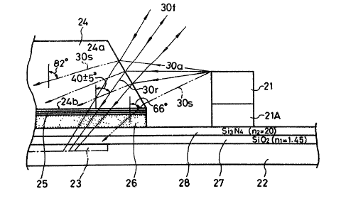
Fig. 1 is an enlarged cross-sectional view showing a
main portion of a semiconductor laser apparatus according to
the present invention which comprises a semiconductor
substrate 22 made of silicon or the like, a semiconductor
laser diode 21 fixed on the semiconductor substrate 22 by a
solder 21A, a photodetector section 23 formed on the
substrate 22 and a prism 24 which is located on the
photodetector section 23 and has a first semitransparent
reflecting plane 24a facing to the laser diode 21 and an
optical disc, not shown, with a predetermined angle and a
plane 24b facing to the photodetector section 23. By the
way, although only one photodetector section 23 is shown in
Fig. 1, there are actually 3 photodetectors formed on the
semiconductor substrate 22.
Further, on the plane 24b, that is, the bottom plane of
the prism 24 a half mirror 25 is formed by multicoating
which constitutes a second semitransparent reflecting plane
of the prism 24. On the upper surface of the semiconductor
substrate 22 there are formed a first coating layer 27 made
of SiO2 (Silicon Dioxide) and a second coating layer 28 made
of Si3N4 ~Silicon Nitride). The above-mentioned half mirror
25 is adhered to the second coating layer 28 by a bonding
agent 26.
In the present embodiment, the refractive index n of
the bonding agent 26 is selected to be almost equal to that
~ ~ ~740~
of the p~ism 24, e.g. 1.56. The refractive index n1 of the
first coating layer 27 and the refractive index n2 f the
second reflective layer 2~ are respectively set at 1.45 and
2Ø
~e thickness d1 of the first coating layer 27 is
selected as 3720 A and the thickness d2 f the second
coating layer 28 as 1128 A~
These first and second coating layers 27 and 28 are
respectively formed by vacuum evaporation techniques or the
like in the predetermined thickness after the photodetector
section 23 and so on are formed on the semiconductor
substrate 22.
The main portion of the semiconductor laser apparatus
is constituted as described above, so that a laser light or
beam 30a radiated from the laser diode 21 is reflected by
the semitransparent reflecting plane 24a arranged in front
of the prism 24 and irradiated on an optical disc and so on,
not shown, as a laser light or beam 30f. A returning laser
light 30r reflected by the optical disc passes through the
same optical path, enters into the prism 24 through the
first semitransparent reflecting plane 24a and irradiates
the photodetector section 23 through the first and second
coating layers 27 and 28 although a portion of the returning
laser light 30r is reflected by the half mirror 25 arranged
on the bottom plane of the prism 24 at an incident angle of
40o + 5O.
On the other hand, a portion of the laser beam 30a
radiated from the laser diode 21 passes through the
semitransparent reflecting plane 24a of the prism 24 and
enters into the prism 24 as a stray laser light 30s as
~ -~t~74(~j~
indicated by a two-dot chain line in Fig. 1. The incident
an~le thereof at that time is made to be approximately from
66O to ~2O
By the way, in the semiconductor laser apparatus
according to the present invetion, since the first and
second coating layers 27 and 28 are formed on the boundary
between the semiconductor substrate 22 and the prism 24, as
will be later described, it is possible that the stray laser
light 30s is almost totally reflected by the first and second
reflecting layers 27 and 28 and thereby does not reach the
photodetector section 23.
Fig. 2 shows how the laser light (7800 A) passes
through the coating layers 27 and 28 when the coating layer
27 is made of Sio2, the refractive index nl of which is
selected as 1.45 and the thickness of which is selected as
3720 A, and the coating layer 28 is made of Si3N4, the
refractive inde2 of which is selected as 2.0 and the
thickness of which is selected as 1128 A.
Fig. 3 shows a relationship between the transmittance
of the laser light and its incident angle a, wherein the
ordinate represents the transmittance and the abscissa the
incident angle a, respectively.
As is understood from Fig. 3, according to the two
coating layers 27 and 28 of the present invention, as shown
by a solid line curve, the transmittance more than 90% is
presented for the laser light, the incident angle a of which
is made as 40O t 5, that is, the returning laser light 30r
from the optical disc, while for the stray laser light 30s,
the incident angle of which is 66 or more, the
transmittance is reduced to less than several %, that is,
~ ~7~0~
the stray laser liqht 30s is subjected to almost total
reflecticn ~y the two coating layers.
Therefore, the photodetector section 23 presents
against the returning laser light 30r a high sensitivlty,
while almost never responds to the stray laser light 30s, so
that it is possible to detect the information contained in
the reflected laser light fro~ the optical disc with a high
sensitivity.
Incidentally, the above data in the graph of Fig. 3 is
made for a so-called S-polarized light of the laser light,
the plane of polarization of which is in the direction
perpendicular to the plane of incidence. While, in Fig. 3 a
broken llne curve represents the data for a P-polarized light
of the laser light. In Fig. 3, a one-dot chain line curve
shows an average data between those for the P-and
S-polarized li~hts. Thus, the variation in the
transmittance with respect to the incident angle a shows the
nearly same tendency as above when average data of
S-polarized light data and P-polarized light data are
concerned.
In addition, the characteristic shown by a fine two-dot
chain line in Fig. 3 shows the case where a single coating
layer only is formed on the substrate 22 without the first
coating layer 27 ~or dl = 0) formed on the same. In this
case, it can be seen that the transmittance scarcely varies
as the incident angle a changes up to 70 so that it cannot
be expected that the photodetector has the selecting
function for the returning laser light.
Figs. 4, 5 and 6 show the characteristics of the
transmittance depending upon the incident angle ~ of the
~7~
laser light when the thicknesses d1 and d2 of the first and
second coating layers 27 and 2~ are varied, respectively.
Ill these embodiments, the ratio of the transmittance
for the returning laser light to that for the stray laser
light is inferior as compared with that of the embodiment
shown in Fig. 3. However, the selecting effect on the
returning laser light is enhanced and the sensitivity of the
photodetector section can be improved as compared with the
case where no coating layer is provided or a single coating
layer is provided.
As the explanation set forth above, in the
manufacturing process of the semiconductor laser apparatus
according to the invention wherein the laser light source,
the photodetector and the prism are integrally formed on the
semiconductor substrate to reduce the size of the optical
head, two coating layers are formed on the boundary between
the prism and the semiconductor substrate in a manner that
the coating layers are provided to present the total
reflection against the stray laser light incident on the
prism, to thereby produce an effect o~ improving the
sensitivity of the photodetector for the returning laser
light from the optical disc.
Further, if the above-mentioned semiconductor laser
apparatus is used as the optical head, it is possible to
detect a tracking error signal, a focus error signal and so
on with a high accuracy.
The above description is given on a single preferred
embodiment of the invnetion but it will be apparent that
many modifications and variations could be effected by one
skilled in the art without departing from the spirit or
1~774~i
scope of the novel concepts of the invention so that the
scope of the invention should be determined by the appended
claims only.
-- 10