Note : Les descriptions sont présentées dans la langue officielle dans laquelle elles ont été soumises.
3767
- 1 -
DOWNSTREAM APPARATIJS AND TECHNIQUE
Background-of the Invention
1. Field of the Invention
This invention relates to semiconductor material
processing and, in particular, to the etching of
semiconductor materials.
2. Art-Background
Removal techniques, e.g., etching and cleaning,
are universally practiced on semiconductor materials, metal
materials, and/or dielectric materials in the production
of electronic devices and/or materials. secause of the
importance of these procedures, extensive research has been
expended in improving established techniclues and developing
novel approaches. Through this research, processing times
have been significantly diminished, and the quality of
these processes has been substantially improved.
One approach that has been used for decreasing
processing times is the simultaneous treatment of a
plurality oE substrates, e.g., semiconcluctor substrates or
semiconductor substrates that have been processed and that
have various levels including metal, semiconductor, and/or
insulator regions. A significant problem, however, occurs
when a plurality o substrates i5 treated. (Substrates,
for the purpose of this invention, comprehend any body upon
which a device is fabricated, inclucling, but not limited
to, devices in process, substrates utilized in
semiconductor device fabrication, and substrates utilized
in the manufacture of hybrid integrated circuits.) This
problem, denominated the loading effect, is characterized
by a change in removal characteristics produced by the
presence of a substrate area significantly larger than that
of a single substrate, i.e., the presence of several
substrates. The loading effect often is manifested both
locally and globally. The local loading effect leads to
non-uniformities across each substrate. For example, in
integrated circuit fabrication, often more material at the
'i ~
-- 2 --
periphery of a substrate is removed than at the center of
the substrate with a concomitant unacceptable non-
uniformity.
In the global loading effect, all substrates of a
batch are etched at the same rate and yet this rate differs
from the rate achieved when a different number of
substrates is treated. This effect is quite
disadvantageous since the etching conditions must be
adjusted or the time varied for the particular number of
substrates that is to be treated. The result of each
loading effect is either a significant increase in
processing time, and thus expense, or the production of
substrates that are unacceptable for electronic devices.
Since the processing of a plurality of substrates
presents many difficulties, techni~ues are being employed
that are adapted to the processing of individual
substrates. For example, excellent etching is produced
using species generated in a plasma and directed by
electric fields towards the substrate that is immersed in
2~ the plasma. Exemplary processes and apparatllses are
described in, ~or example, U. S. Patent 4,383,8~5, issued
Ma~ 17, 1983. A seco~d approach that has been utilized and
described in Journal of the Electrochemical Society, 129,
S. Dzioba et al, page 2537 (19B2), Proceedings of the
7th Conference of Solid State Devices, Y. Horiike and
M. Shibagaki, Tokyo t1975), supplement to the Japanese
Journal of A~lied Physics, 15, page 13 (1976), and Thin
Film Processes, Chapter V-2, C. M. Melliar-Smith and
C. J. Mogab, Academic Press, edited by J. L. Vossen and
W. Kern, New York (1978) is the separation of the substrate
from the region where the etching species is produced. In
such a process, a discharge is established in one region
and the etching species produced in this discharge is
allowed, generally through diffusive and bulk flow
processes, to leave the discharge region and to induce
etching or cleaning of the substrates in a second, disjoint
region. This downstream process has been employed
8767
generally to prevent the plasma from damaging the substrate.
For example, when a substrate is present in the plasma region,
it is subjected to bombardment by kinetically energetic
species. These energetic species often induce sputtering of
substrate material. The radiation and fields associated with
the plasma also have the potential for inducing damage.
Despite the reduction of damage to the substrate, attempts to
expand downstream removal techniques to multiple substrates
have led to loading effects, and thus the techniques presently
employed remain, to a large extent, repetitive single substate
methods.
Summary of the Invention
In accordance with an aspect of the invention there
is provided a process for fabricating a device including the
procedure of removing material from a plurality of substrates
comprising the steps of producing reactive species in a plasma
and directing said species to said substrates and subsequently
into an effluent wherein said substrates are disjoint from and
not surrounded by said plasma characterized in that the volume
of said plasma is at least 200 percent as large as the volume
occupied by said substrates, and the concentration of said
reactive species measured in said effluent in the absence of
said substrateSis at least 25 percent of the concentration of
said species at the periphcry of said plasma.
~3y carefully configuring an apparatus and
controlling the removal process, e.g., the etching and/or
cleaning process, the advantages of downstream removal are
producible with multiple substrate treatment while the
disadvantages associated with the loading effect are avoided,
i.e., etch rates across a substrate and from substrate to
substrate do not vary more than 20 percent. Highly
desirable results are produced by ensuring that 1) the
substrates do not contact or are not surrounded by
~,
.: ..., .., r~
l-~t787~7
- 3a -
the plasma, 2) the volume of the discharge region is at
least 200 percent of the volume occupied by the substrates,
and 3) the etchant species concentration exiting the
etchant chamber when no substrates are present should
be not less than 25 percent of the etchant species
concentration at the boundary of the discharge region.
By conforming to these three criteria up to 48 substrates
have been etched without substantial loading effect
difficulties, and this number has not been limited,
except by weight and space considerations.
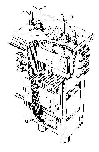
Brief Description of the Drawing
_ _ __ _ __ ___ ~__ ___
The Figure is illustrative of an apparatus
involved in the invention.
Detailed Descri~tion
_________ _ _ _ _
The downstream reactor and reaction process of
B7~7
-- 4 --
the invention should satisfy three criteria. First, the
substrate should not contact or be surrounded by the
plasma. To fully define the limits of this criterion, it
is necessary to specify the region that is considered
occupied by the plasma. In particular, the discharge
region is defined by all points that have a luminosity due
to the discharge and that are at least 5 percent as
intense as the most luminescent point produced by the
discharge. The luminosity of a point is easily measured
using conventional detectors such as photomultipliers or
photodiodes combined with, for example, bandpass filters.
Thus, to define the discharge region, all the luminescent
points produced by the discharge are measured. The point
of highest luminosity is taken as a reference, and the
discharge volume is defined by all points whose luminosity
is greater than or equal to 5 percent of this highest
value.
Many configurations satisfy the first criterion.
For example, the configuration shown in the Figure is
satisfactory and easily employed. It should be noted that
the means utiliæed for producin~ the discharge generally
determines its size. ~or example, discharges are
producible by utilizing r.~. power, dc power, or microwave
power. The region into which power is channeled by
expedients such as electrodes, 10, is generally
representative of the area in which luminescence occurs.
(See Techniques and A~plications of Plasma Chemistry,
J. R. Hollahan and A. T. Bell, Wiley-Interscience,
New York (1974) for a description of various techniques
useful for producing a discharge suitable for removal
techniques.) The substrates, 20, are then located in a
spatial region that is disjoint from the discharge region
and which is not surrounded by the discharge region. For
example, a configuration is not suitable where the
substrates are surrounded by the discharge. In contrast,
the configuration of the Figure is suitable since the
discharye, in area 15, produced by power introduced through
-- 5
electrode, 10, is disjoint from the substrates, 20, and
does not surround the substrates.
Since reactive species should reach the surface
of the substrate to induce removal, it is not desirable
that the substrates contact each other. Generally, the
substrates are held apart by a holder, 25, that is
typically formed from an inert material such as aluminum or
fluorocarbon. The spacing between the substrates chosen to
ensure reactive species contact is not critical. However,
it is generally desirable to have spacings in the range 5
to 15 mm. Larger spacings are undesirable since they
require excessive space, and smaller spacings are
undesirable because they restrict mass transport and cause
excessive pressure drop. It is also typically advantageous
to position the substrates so that they are parallel or
within 5 degrees of parallel. Use of a non-parallel
configuration, although not precluded, is not as desirable
because it induces non-uniform gas flow.
To avoid the loading effect, a second criterion
should also be satisfied. In particular, the volume of the
discharge region, as previously defined, should be at least
100 percent, preferably at least 200 pe~cent, of the volume
occupied by the substrates. The volume o~ the substrates
is defined by the region encompassed by connecting every
point on the periphery of each substrate with every point
on the periphery of every other substrate. The outer
boundaries of this subtended region are the ambit of the
substrates. Typically, plasma discharge volumes in the
range 2 to 10 liters are utilized. Larger volumes require
excessive power while smaller volumes are less power
efficient. Therefore, the substrates for typical operating
parameters should generally occupy a volume in the range 1
to 5 liters. Silicon substrates typically have a diameter
in the range 100 to 150 mm. Therefore, to satisfy the
volume requirements for typical operating parameters,
average spacings between the substrates are generally in
the range 5 to 10 mm for the simultaneous processing of 10
787Co'7
-- 6
to 30 silicon substrates.
The third criterion is satisfied if the
concentration of the reactive species in the effluent
exiting the reaction chamber, i.e., the chamber in which
the substrates are located, when no substrates are present,
is not less than 25 percent of the etchant species
concentration at the boundary of the previously defined
discharge region. The concentration levels at the removal
chamber exit and at the periphery of the discharge region
are measurable using conventional detectors such as
catalytic probe detectors. (Catalytic probe detectors and
their use are described in Canadian Journal of Chemistry,
.
37, L. Elias et al, page 1690 ~1959) and Progress ln
Reaction Xinetics, 1, F. Kaufman, Pergamon Press, New York
(1961).) A reactive species is defined as a species which
causes removal of material from the region to be etched or
cleaned by processes includinq ablation by abstraction,
insertion, and/or reaction and desorption. If more than
one reactive species is generated, then the satisfaction of
2Q the third criterion is determined by summiny the reactive
species concentrations. ~or example, in the etching of
silicon, a gaseous discharge is produced in 1) CF4
combined with ox~gen or ~) N~3. rhis discharye induces
the Eormation of fluorine atom etchant species which, in
turn, produces etching through the contemplated reaction of
fluorine atoms with silicon to Eorm gaseous SiF4.
The distance between the discharge region and the
substrate, as well as the discharge power and gas pressure
and flow, all affect the satisfaction of the third
criterion. It is typically desirable to utilize discharge
powers in the range 100 to 1500 Watts with a distance
between the discharge and the substrate in the range 1 to
10 cm (measured between the downstream boundary of the
discharge and the upstream edge of the substrate) to yield
suitable concentrations of reactive species. The
concentration of the gas that is the precursor to the
reactive species, i.e., that undergoes an interaction in
-- 7 --
the plasma to produce a species capable of reaction, also
affects this third criterion. Typically, for the power
levels and discharge and substrate distances discussed,
etchant precursor gas pressures in the range 66.7 to
666.6 Pa (0.5 to 5 Torr) are desirable. ~igher pressures
generally lead to inhomogeneities, while lower pressures
produce large proportionate pressure differentials across
the substrates and tend to induce sputtering of material
from the chamber walls. It is also possible to combine the
gas reactive species precursor with an inert gas.
Typically, inert gases such as He, Ar, and N2 are
utilized, and total pressures of inert gas and precursor
gas in the range 133.3 to 1333 Pa ~1 to 10 Torr) are
suitable.
As previously discussed, the reactive species are
caused to flow from the discharge region to the substrates.
This flow is easily accomplished by producing a pressure
differential through conventional techniques such as the
use of a vacuum ~ump. Other means, such as the use of
diffusion of the species Erom one concentration region to a
second, are also possible.
Although the criteria previously discussed are
those that should b~ satisfi~d Eor the practice of the
subject invention, there are other expedients that are
useful, although not essential, to the invention. For
example, it is desirable to coat the reaction chamber walls
with a fluorocarbon material such as Teflon M or
KynarTM. This material retards the recombination of
reaction species and therefore aides in the satisfaction of
the third criterion. It is also desirable to use a high
frequency in the range 13.56 to 27.12 MHz for producing an
r.f. gas discharge. The use of high frequencies produces a
more uniform plasma and results in a low sheath voltage.
This low voltage limits the potential energy of various gas
species and thus reduces any sputtering that is present.
The following examples are illustrative of the
invention.
-- 8 --
Example 1
Forty-eight aluminum oxide ceramic substrates
measuring 5.53 cm x 6.93 cm x 0.051 cm
(3.75 inches x 4.50 inches x 20 mils) were fire-cleaned in
an air ambient at 1500 degrees C. An AZ-1350J resist
solution, as provided by American Hoechst Company, was
diluted 4:1 in AZ thinner, also provided by American
Hoechst. Each substrate was spun at 200 rpm, and a
sufficient amount of this solution was placed on each of
the spinning substrates to cover it. The speed of the
substrates was then increased to 3000 rpm, and the spinning
was continued for approximately 25 seconds. This procedure
resulted in a resist layer of about 1 ~m in thickness. The
resists were baked at approximately 80 degrees C in an air
ambient oven and maintained at this temperature for
approximately 30 minutes. The substrates were placed in
the substrate holder, 25, of the etching apparatus, and the
apparatus was evacuated to a pressure of approximately
2.7 Pa (20 mTorr~. ~he spaciny between the substrates in
the substrate holder was approximately 0.48 cm ~3/16 of an
inch).
~ mixture Oe 3.6 mole percent C~4 in oxygen was
introduced through inlets, 30. The combined flow through
the inlets was approximately 470 sccm. The resulting
pressure in the discllarge chamber was approximately
80 Pa (0.6 Torr). Approximately 400 Watts of r.f. power at
27.12 MHz was applied to the electrode, 10, through
leads, 40, while cooling water was supplied to the
electrodes through the inlets, 35, in leads, 40. (The
electrode was electrically isolated from the case and
vacuum sealed from the ambient by insulators, 50.) Etching
was continued until the resist layer was removed. Etching
was uniform in the two directions perpendicular to the gas
flow direction and showed a slight non-uniformity in the
direction parallel to the ~low direction due to inadequate
bulk flow velocity. This slight non-uniformity--evidenced
by a tendency to strip at a greater rate at the periphery
~'~'7~
of the substrate closest to the discharge region and
oriented normal to the flow direction--is rectifiable by
increasinq the pumping speed and gas flow rate.
Example 2
The procedure of Example 1 was utilized except
the substrate was coated with 40 nm of tantalum nitride
(Ta2N), rather than with the resist material.
Additionally, the gas introduced through inlets, 30, was
12 mole percent oxygen in CF4. Removal of the tantalum
nitride proceeded essentially uniformly in all directions.