Note : Les descriptions sont présentées dans la langue officielle dans laquelle elles ont été soumises.
8~3~72
LWCS 210534
DIVERSITY RECEPTION RADIO RECEIV:ER
This invention relates to the ~ield of wireless receivers ~or
mobile communications. More particularly, it relates to a radio
receiver system employing diversity switching to automatically
select among the outputs of a plurality o~ receivers, such as
twin receivers, and to improve communication quality when the
strengths of the electromagnetic signal waves reaching the re-
ceiver system are subject to large scale fluctuations.
An object of the invention is to provide a diversity reception
receiver that reduces unwanted switching noise in a recovered
signal when both signals waves are weak or strong. A more par-
ticular object of the invention is to reduce the unnecessary
"churning" of prior art diversity receivers when both signals are
relatively weak and the unnecessary switching that saturates the
signal-to-noise (S/N) performance when both signals are relative-
ly strong.
In keeping with an aspect o~ the invention, a diversity reception
radio receiver has a two-receiver system incorporating ~irst and
second receivers. A wave envelope detector is provided ~or each
receiver to generate an output voltage corresponding to the
strength of the electromagnetic signal wave which is p:icXed up by
~133~7~
66446-403
the receiver. A hysteresls comparator compares the outputs of the
two wave envelope detectors and generates a switching control
signal. The hysteresis comparator changes a threshold level of
change in response to the strength of the output of either one of
the two ~7ave envelope detectors. Responsive to the switching
contro] signal, a switching means se Lects between the signals
which are produced by the first and second receivers. Switching
between the first and second recovered signals occurs only a~ter
the compared outputs reach the threshold level.
The above mentioned and other features oi this invention
and the manner of obtaininy them will become more apparent, and
the invention itself wil:L be best understood by reference to the
followlng description of some embodiments of the invention taken
in conjunction with the accompanyiny drawings, in which:
Fiyure 1 is a simplified diagrammatic block diagram of a
first embodiment of my invention;
Figure 2 shows typical detector output voltages of weak
signal waves from the two receivers which are used in the
embodiment of Figure 1, together with a trace indicating which
receiver output wi:Ll be selected hy automatic switching;
Figure 3 shows typiaal deteator output voltages of
strony siynal waves from the two receivers which are used in the
embocli-
~2~33~
LWCS 210534
ment of Figure 1, together with a trace indicating which receiveroutput will be selected by automatic switching;
Figure 4 shows a graph of the noise level o~ the embodiment
of Figure 1 as a function o~ the average signal strength of the
received electromagnetic wave~, together wlth a comparison o~ the
noise level of a prior art receiver shown in Figure 7;
Figure 5 is a simpli~ied diagrammatic schematic of the
embodiment of Figure 1, showing details of the controller and
comparator;
Figure 6 is a simplified diagrammatic ~locX diagram of a
second embodiment of my invention employing a digital controller;
and
Figure 7 is a block diagram of a prior art diversity re-
ceiver employing automatic switching between two receivers.
The block diagram of Figure 7 shows a prior art diversity recep-
tion receiver ~or ~requency modulated ~FM) signals. The FM
modulated signals are picked up by a separated pair of antennas 1
and 2 and are respectively input to a pair o~ demodulating re-
~283~72
~.WCs 210534
ceivers 3 and 4, which in turn recover baseband ~ignals Sl and S2from the picked up modulated signals.
For determining the received signal strength, each receiver iII-
cludes a wave envelope detector tnot shown) for detecting the
wave envelope of the antenna signals which it receives. These
wave envelope detectors respectively generate detector output
voltages vl ~receiver 3) and v2 ~receiver 4) which are propor-
tional to the strengths of the electromagnetic waves picked up
from their respective antennas 1, 2.
These detector output voltages v1, v2 are input to a comparator 5
which generates a signal for directing baseband switch 6 to
select the output o~ the ~aseband receiver having the larger
detector output voltage. The base~and signal selected by switch
6 is amplified by a baseband amplifier 7 and then used to drive
an output speaker 8. In sum, this prior art twin receiver system
automatically switches to the stronger of two recovered signals
in response to a comparator circuit's indication as to which
receiver has the larger wave envelope detector output voltage.
However, such a prior art diversity receiver does not perEorm
well when the electromagnetic signals picked up by each of the
two antennas are relatively weak with a high content o~ back-
ground noise. In such a case, the envelope detector signals are
correspondingly noisy. Thus, even if the inputs to the two
i~3~ LWCS 210534
receivers are about the same quality, the noise can cause unnec-
essary automatic switching between the receivers. The noise
generated by this unnecessary switching further weakens the sig-
nal-to-noise ratio (S/N) of the recovered signal.
Moreover, there are also problems when the signals picked up by
both antennas are relatively strong. In such a case, even a
significant drop in wave amplitude may not cause much degradation
in an already good S/N. However, the prior art circuit continues
to automatically search for and switch to the stronger signal,
giving rise to more switching than needed. This causes addi-
tional "switching noise" that degrades the recovered signal,
leading to an undesirable saturation of S/N for strong signals
(see Fig. 4).
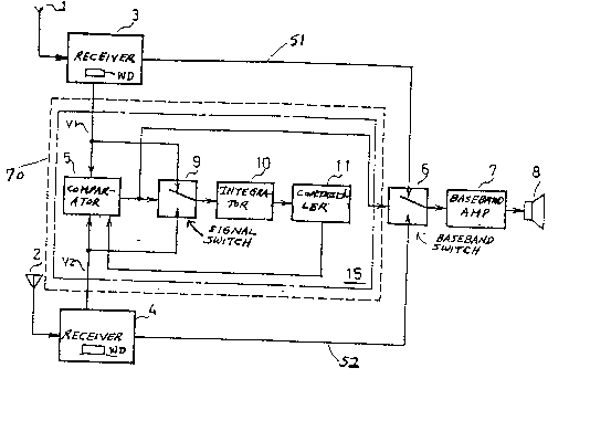
Figure 1 shows a block diagram of a first embodiment of my inven-
tion providing a diversity receiver which is suitable for FM
signals. The FM modulated signals are picked up by a pair of
antennas 1 and 2 which are separated from each other. The sig-
nals are respectively input to a pair of demodulating receivers 3
and 4, which in turn recover baseband signals Sl and 52 from
them. The recovered baseband signals Sl and S2 are input to
basehand switch 6, which selects one of them to be fed via base-
band amplifler 7 to output speaker 8.
lZ83~2 LWCS 210534
Each receiver includes a wave envelope detector WD for detecting
the wave envelope o~ the antenna signals which it receives, and
hence for detecting their signal strength. These wave envelope
detectors respectively generate detector output voltages vl (re-
ceiver 3) and v2 ~receiver 4), which voltages are proportional to
the strengths of the electromagnetic waves input from their
respective antennas 1, 2.
A dotted line 70 encloses parts constituting an improved compara-
tor portion of the invention. A comparator 5 in a comparator
circuit 15 receives the envelope detector voltages v1 and v2 and
simultaneously sends switching control signals to both baseband
switch 6 and signal switch 9.
The detector output voltages vl, v2 of receivers 3 and 4 ar~ also
split off as alternative inputs to signal switc~ 9. The output
selected by switch 9 goes to an integrator or low pass ~ilter 10,
which smoothes or time-averages the selected detector output
voltage. The output of integrator 10 is an input to controller
11, which generates a control signal that is an additional input
to comparator 5 in order to give it a predetermined amount of
hysteresis or a threshold resistance to change, that is respon-
sive to the smoothed wave envelope detector output voltage pro-
duced by integrator 10.
~2~3~2 LWCS 210534
The first embodiment operates this way. As shown in Figure 1,
the circuit is such that every time comparator 5 sends a control
signal to reverse the position of baseband switch 6, it also
simultaneously sends a corresponding control signal to reverse
signal switch 9. For example, if comparator 5 orders baseband
switch 6 to select receiver 3, as having the stronger received
signal, it also simultaneously orders signal switch 9 to select
the detector OUtp~lt voltage vl to be fed to integrator 10.
Conversaly, if switch 6 is ordered to select receiver 4, output
voltage v2 is fed to integrator 10. Integrator 10 then produce~
a smoothed output signal that is a time-averaged version of which
ever detector output voltage is then being received by it and
feeds such smoothed signal to controller 11. This smoothed
signal reflects the strength of the signal waves. Controller 11,
in turn, generates a control signal for comparator 5 that causes
it to ma~e a corresponding change in the amount of its hysteresis
or threshold resistance to change, depending on the strength of
the received signal.
For weaX signal waves, Figure 2 shows typical wave envelope
detector output voltages which vary as a ~unction of time. These
output voltages are from the two receivers used in the embodiment
o~ Figure 1, together with a trace indicating which receiver
output will be selected by comparator 5.
~2 ~3~2 LWCS 210534
Starting on the left of Figure 2, initially vl is greater than
v2, so receiver 3 is selected. However, because of the hystere-
sis or threshold resistance to change which is set in comparator
5, that comparator will not order a switchover to receiver
until after the detector voltage vl falls below dekector voltage
V2 by some specific amount d. If the amount of hysteresis or
threshold resistance to change d is larger than the typical noise
voltage that appears in the detector outputs, unnecessary switch-
ing between the receivers can be virtually eliminated.
For strong signal waves, Figure 3 shows typical wave envelope
detector output voltages which vary as a function of time. These
two voltages are provided by the two receivers used in the embod-
iment of Figure 1. Figure 3 also includes a trace indicating
which receiver output is selected by comparator 5. Because the
threshold resistance to change d' in comparator 5 has been set
much larger than it was set in Figure 2, there will be no switch-
over of receivers unless the difference in detector output volt-
ages becomes unusually large. Therefore, compared with the si-
tuation for weak signals, the frequency of switching has greatly
diminishe~.
Figure 4 shows a graph of the noise level of the embodiment of
Figure 1 as a function of the average signal strength of the
received electromagnetic waves, toyether with a comparison of the
LWCS 210534
noise level of the prior art receiver of Figure 7 (dotted line).
From this graph, it is clear that the introduction of a control-
led amount of hysteresis or threshold resistance to change gener-
ally reduces the noise, particularly ~or strong signal waves.
Figure 5 is a simplified diagrammatic schematic of the embodiment
of Figure 1, showing details of the controller and comparator.
FM receivers 3 and 4 recover the modulated signals picked up by
antennas 1 and 2 and deliver them as baseband signals Sl and S2
that become the alternative inputs to baseband switch 6. To help
determine which signal is better, the respective wave envelope
detector output voltages vl, v2 from receivers 3 and 4 are input
as alternatives to signal switch 9.
Figure 5 shows the case where receiver 3 has been selected and
the detector output voltage vl has been input to a law pass
smoothing filter 10. The output of low pass filter 10 is being
input to the "+" side of comparators 21, 22, & 23.
Comparators 21 - 23 and their associated logic network are for
determining when the signal waves are "weak", "mid-strength", and
"strong". The "-" inputs o~ comparators 21 and 22 are provided
with reference voltages obtained by voltage dividers respectively
formed by potentiometers 41, 42 and resistors 44, 45 connected
~z~3~ LWCS 210534
between a supply voltage Vcc and ground. The potentiometers are
set to adjust for the characteristics of the particular wave
detectors (not shown) that produce the detector output voltages.
The "-" input of comparator 23 is grounded by resistor 46.
The reference voltage input to comparator 21 is set higher than
the reference voltage input to comparator 22. For example,
suppose comparator 21 is set for a received detector output
voltage of 20 dB microvolts and comparator 22 is set ~or 10 dB
microvolts. Further suppose the voltage input from low pass
filter 10 is 20 dB microvolts or more, indicating a "strong"
signal wave. Then the outputs of all three comparators 21 - 23
will become logical l's. This will cause the outputs of Exclu-
sive OR gates 26 and 27 to become 0's. A logic network at the
inputs of a set of controllable switches 32 - 37 is arranged so
that when both gates 26 and 27 output 0's, only switches 32 and
35 will be "CLOSED", the others being left "OPEN".
Suppose that the voltage input from low pass filter 10 is between
10 dB - 20 dB microvolts, indicating a "mid-strength" signal
wave. The comparator 21 gives an output which is a 0, but com-
parators 22 and 23 continue giving outputs which are lls. This
causes Exclusive OR gate 26 to give an output which is a 1, but
Exclusive OR 27 continues to output a 0. For the logic network
whlch ls shown, the outputs o~ the gates cause only switches 33
33~2
LWCS 210534
and 36 to be fed control input signals of 1, thus switching them
"CLOS~D" and leaving the others "OPEN".
When the voltage input from low pass filter 10 equals or falls
below 10 dB microvolts, it indicates a "weak" signal wave.
Comparators 21 and 22 then give outputs which are 0's, while only
comparator 23 will continue to give an output which is a 1.
Therefore, Exclusive OR 26 gives an output which is a 0 and
Exclusive OR 27 gives an output which is a 1. This causes only
switches 34 and 37 to be l'CLOSED'I, the others being le~t 'IOPENII.
The responses of the logical network described above are summar~
ized by Table I.
~L~8~L72
LWCS 210534
TABLE I - RESPONSE OF LOGIC NETWORK
__ ______________________________ ________
SIGNAL WAVE STRENGTH
GATE WEAK MID- STRONG
OUTPUT STRENGTH
__________________________________________
21 0 0
_______ __________________________________
22 0
__________________~_______________________
23
__________________________________________
26 0 1 0
__________________________________________
27 1 0 0
__________________________________________
SWITCH
POSITION
__________________________________________
32 OPEN OPEN CLOSED
___________ ______________________________
33 OPEN CLOSED OPEN
__________________________________________
34 CLOSED OPEN OPEN
________________________________ _________
OPEM OPEN CLOSED
__________________________________________
36 OPEN CLOSED OPEN
__________________________________________
37 CLOSED OPEN OPEN
__________________________________________
~L2~3~L7~:
LWCS 210534
In Figure 5, comparator circuit 5 is shown as including two
comparators 24 and 25 having "-" inputs respectively receiving
wave envelope detector output voltages vl and v2. The "-~" inputs
of comparakors 24 and 25 receive the corresponding "other" wave
envelope detector output voltage v2 or vl, as proportionally
reduced by the voltage divider networks leading to these "~"
inputs. Thus, comparator circuit 5 is called a "h~steresis
comparator".
one end of each of the resistors 50 and 54 is respectively con-
nected to to the "~" input of comparators 24 and 25, and the
other end of each resistor is connected to ground. Controllable
switches 32 - 37 effectively switch resistors 47 - 49 and 51 - 53
into and out of the voltage divider circuits connected to the "+"
inputs of comparators 24 and 25. Thus, switches 32 - 37 set the
relative values of the resistors making up the voltage dividers
connected to the "~" inputs, thereby adjusting the amount of
hysteresis that is exhibited by comparators 24 and 25.
gl283gL~
LWCS 210534
To enable the hysteresis operation described above, resistors
47 - 49 and 51 - 53 should preferably have the following
relationships:
resistor 47 > resistor 48 > resistor 49
resistor 51 > resistor 52 > resistor 53
The output of comparators 24 and 25 is input through respective
input diodes 30 and 31 to a bistable multivibrator 74. For
example, suppose receiver 3 is selected by switches 6 and 9
because vl > v2 by an amount exceeding the current hysteresis or
threshold resistance to change. This means that comparator 24 is
producing a "O" and comparator 25 is producing a "1". Bistable
74 then has its left transistor 28 IIOFF" and its right transistor
29 "OM", which can be interpreted as outputting a logical "O" to
the control input of switch 6 which selects the recovered signal
Sl.
Next, suppo3e that wave envelope detector output voltage vl
becomes less than detector output voltage v2, by an amount ex-
ceeding the current hysteresis or the threshold resistance to
change. Comparator 24 switches from "O" to lll'l, causing a posi-
tive pulse to pass through diode 30 to the base o~ the bistable's
14
~L;~33~L'7;2 LWCS 210 5 3 4
transistor 28, flipping bistable 74 so that left transistor 28
becomes "ON" and right transistor 29 becomes 'IOFF". Bistable 74
then has an output which is a logical "1" and which controls
switch 6 to select recovered signal S2 from receiver 4. This
output of bistable 74 also controls switch 9, via line 76, to
select detector output voltage v2 as input for integrator 10.
Figure 6 is a simplified diagrammatic block diagram o~ a second
embodlment of the invention employing a digital controller. It
has a comparator circuit 16 which includes an analog-to-digital
converter 12, a digital controller 13, and a digital-to-analog
converter 14. The digital controller 13 could be, for example, a
microprocessor based controller.
The first embodiment of Figure 5 quantizes the strength of the
signal waves into three levels: wea~, mid-strength, and strong.
It also quantizes the amount of hysteresis into three alterna-
tives. The second embodiment of Figure 6 provides virtually a
continuum of hysteresis adjustments, by means such as a computa-
tion or table look up by the digital ~ontroller; thus, such a
continuum o~ adjustments i5 within the scope of the invention.
As will now be apparent, my invention uses a comparator that has
hysteresis ~or providing the output signals responsive to the
wave envelope detectors. The amount of hysteresis is adjusted in
~83~2
L~CS 210534
response to the strength of the received signal waves. This
substantially reduces the frequency of switching between the
alternative recovered signals, greatly reducing the noise which
is introduced into the recovered signal by the switching between
receivers, both when the signals are weak and when they are
strong.
While the principles of the invention have been described above
in connection with specific apparatus and applications, it is to
be understood that this description is made only by way o~ exam-
ple and not as a limitation on the scope of the invention.
16