Note : Les descriptions sont présentées dans la langue officielle dans laquelle elles ont été soumises.
~s~o~
Cable arrangement or use in a multlplex transmission
system
The present invention relates to a cable arrangement
in which a pair of power conductors for transmitting power
and a pair of signal conductors for transmitting various
signals are integrally formed in one cable structure.
To enable the prior art to be described with the aid
of a diagram, the figures of the drawings will first be
listed.
Fig. 1 is a circuit diagram showing an example of
10 multiplex transmission terminal;
Fig. 2 is a perspective view of an example of a wire
connection in a conventional multiplex transmission
terminal;
Fig. 3 is a perspective view showing an example of a
15 multiplex transmission cable according to an embodiment of
the present invention;
Fig. 4 is a perspective view showing a specific
feature of the use of a multiplex transmission cable
according to the present invention;
Fig. 5 is a front view of the terminal shown in Fig. 4
with the casing halves opened, and
Fig. 6 is a perspective view of a terminal attached to
a multiplex transmission cable according to the present
'
.
S703
-- 2
invention.
Fig. 1 shows an example of multiplex transmission
system. In Fig. 1, lOl and 102 denote power transmission
lines for supplying power to terminals 105 and 106. 103
and 104 denote data transmission lines for transmitting
data information to the terminals 105 and 106. In the
example shown, the respective terminals 105 and 106 are
provided with actuators 107 and 108, such as an electric
motor and a display lamp, which are activated by the data,
in addition to various switches lO9 and 110 for inputting
the data.
In the prior art, the power lines 101 and 102 and the
data transmission lines 103 and 104 are connected to the
respective terminals 105 and 106 by means of one or more
separate conventional connecting wires or twisted pair
wires, using external connectors 121 and 122, as shown in
Fig. 2. In Fig. 2, the connecting lines shown generally
by the arrow A are the lines to be connected to a front
stage terminal and the lines shown generally by the arrow
B are the lines to be connected to a back stage terminal.
However, in the prior art, since the respective lines
are connected to the multiplex transmission terminal
through one or more external connectors 121 and 122, in
order to connect each line with the terminal 7 it is
necessary to provide a cable of a suitable length corres-
ponding to the position of the multiplex transmission
terminal, having a suitable connector tip attached to the
ends of the conductors of the cable.
Moreover, since the respective lines lOl and 102 are
laid independently, it is necessary to consider the cable
lay out to prevent noise caused by the power lines from
being induced on the signal lines.
An essential ob~ect of the present invention is to
provide a multiplex transmission cable arrangement that is
capable of eliminating these problems.
9d5~
-- 3
Another object oE the present invention is to provide
a mu]tiplex transmission cable arrangement that is easy to
connect to one or more multiplex transmission terminals.
A further object of the present invention is to
5 provide a multiple transmission cable arrangement that can
avoid interference from the power lines.
To this end, the invention consists of a cable arrange-
ment comprising a pair of power conductors which are
electrically separated but closely adjacent each other; a
10 pair of signal conductors disposed to one side of said
power conductors with the centers of the respective signal
conductors positioned substantially at a level between
said power conductors while extending parallel to the
power conductors; and insulation layers for insulating
15 said power conductors and signal conductors, respectively.
Referring to Fig. 3, there is shown a multiplex trans-
mission cable unit 10 comprising a pair of power supply
conductors 1 and 2 of elongated strip shape extending
parallel to each other. The two conductors 1 and 2 are
20 located as close as possible to each other, while
maintaining the necessary distance for assuring the
required withstand voltage. Disposing the conductors 1
and 2 close to each other increases the capacitance
between them, whereby to provide a low impedance power
25 supply line. A pair of signal conductors 3 and 4 are
disposed on one side of the conductors 1 and 2, at a level
corresponding to the center between the conductors 1 and 2
and extending parallel to and alongside the conductors 1
and 2. The respective distances between the conductor 3
30 and the conductors 1 and 2 are equal to prevent electro-
static induction from the conductors 1 and 2. The
respective distances between the conductor 4 and the
conductors 1 and 2 are also equal.
The conductors 1 to 4 are covered with an insulation
:~.2~5703
_ 4
material 11 (referred to as insulation layer hereinafter),
as shown in Fig. 3. Although the conductors 1 to 4 are
covered with the insulation layer 11 throughout the whole
length of the conductors, a multiplex transmission
terminal can be connected to the conductors 1 to 4
anywhere along the cable, as desired. Grooves 12 and 13
are formed on the surface of the insulation layer 11,
corresponding to interface portions between the power
conductors 1 or 2 and the signal conductor 3, and between
the two signal conductors 3 and 4.
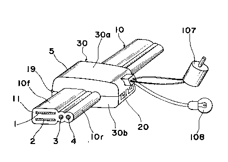
Referring to Figs. 4, 5 and 6, a terminal casing 30 of
a multiplex transmission terminal is composed of a top
half 30a and a bottom half 30b made of a resin material
and connected by one or more hinges 19, so that the halves
30a and 30b can be opened and closed. A lock mechanism 20
is provided at the right hand portion of the outside of
the casing 30. A printed circuit board 25 is accommodated
in the top half 30a, a circuit arrangement, including such
elements as an integrated circuit chip 23 or other
necessary components for use in the terminal, being
provided on the printed circuit board 25. This circuit
arrangement has its respective components connected to a
conductor pattern 24 formed on the printed circuit board
25 to provide a desired terminal circuit.
Three pressing connector pins 15, 17 and 18 project
downwardly from the printed circuit board 25 toward a
recess 26f, and one pressing type connector pin 16
projects upwardly from the bottom casing half 30b towards
the recess 26f. The connector pin 15 is connected to the
circuit pattern 24, and the connector pin 16 is also
connected to other parts of the circuit pattern 24 through
a flexible wire 27. The connector pins 15 and 16 are such
that, when the casing halves are closed, the respective
ends of the pins 15 and 16 project into the cable so that
~29~703
-- 5
the pin 15 is coupled with the power supply conductor 1
and the connector pin 16 is coupled with the power supply
conductor 2. The connector pins 17 and 18 are connected
to other parts of the circuit pattern.
The terminal 30 is mounted on the cable unit 10 in
such a manner that the power conductor portion ]Of is laid
in the generally flat shaped recess 26f and signal
conductor portions lOr are laid in the round recesses
26r. The terminal 30 is then closed, as shown in Figs. 4
and 6, with the casing halves being locked together by the
member 20. The ends of the connector pins 15, 16, 17 and
18 penetrate the insulation layer 11, the pins 15 and 16
contacting the conductors 1 and 2 respectively, and the
pins 17 and 18 clamping and contacting the conductors 3
and 4 by means of their fork shaped ends, as shown in Fig.
6. The respective projections 14 fit in the grooves 12
and 13 which thus serve to position the pins 17 and 18
with respect to the conductors 3 and 4.
An advantage of the present invention is that the
terminal 30 can be mounted anywhere along the cable unit
lO without need for working on the cable, such as cable
cutting or end treatment.
Another advantage of the present arrangement is that,
since the power conductors are closely arranged, it is
possible to decrease the power source impedance,
independently of the length of the cable unit.
A still further advantage of the present arrangement
is that the cable unit has such a structure that cross
talk between the power conductors and the signal
conductors is smal], whereby noise on the signal
conductors caused by the power conductors can be
effectively avoided.