Note : Les descriptions sont présentées dans la langue officielle dans laquelle elles ont été soumises.
1~032~
BACKGROUND OF THE INVENTION
The present invention broadly relates to an optical disk
system having a head actuator adapted for driving the optical
head in the radial direction of an optical disk and, more
particularly, to a device for driving and controlling the
optical head in such an optical disk system. Still more
particularly, the present invention is concerned with a speed
control circuit for conducting speed control of the head
actuator during access to a track.
BRIEF DESCRIPTION OF THE DRAWINGS
Fig. 1 is a block diagram of a control system of a
conventional device for drivlng and controlling an optical
head in an optical disk system;
Fig. 2 is an input-output characteristic diagram of a
reference speed generation circuit shown in Fig. 1;
Fig. 3 is an input-output characteristic diagram of a speed
detection circuit shown in Fig. 1;
Fig. 4 is a waveform diagram of a reference speed output and
a detected speed output obtained in the conventional system;
Fig. 5 is a block diagram of a control system of an optical
head driving and controlling device which represents an
embodiment of the present invention;
Fig. 5 is a block diagram of details of the essential
~, sections of a speed control system shown in Fig. 5;
Fig. 7 is an input-output characteristic diagram of a second
memory circuit shown in Fig. 5;
~13~3Zli~
Fig. 8 is an input-output characteristic diagram of a first
memory circuit shown in Fig. 5;
Fig. 9 is a waveform diagram of a reference speed output and
a detected speed output in accordance with the present
invention; and
Fig. 10 i5 a waveform diagram of outputs during operation
from sections of the speed control system shown in Fig. 5.
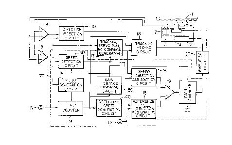
Fig. 1 is a block diagram of the control system in a known
optical head driving and controlling device used in an
optical disk system disclosed in Japanese Patent Application
No. 156526/1986. Referring to Fig. 1, the optical disk
system has an optical disk 1 provided with tracks in the form
of concentric circles or a spiral which carry information. A
light beam which serves as an informatiorl transfer media
between the optical disk 1 and an optical head 3 is denoted
by 2. The optical head 3 is housed in a carriage 4 which is
driven by a head actuator 5 so that it moves across the
tracks on the optical disk 1. The carriage 4 is pro~ided
with a tracking actuator 6 provided with a collimator lens
(not shown) which is adapted to focus
la -
J
,
~03218
the light beam 2 so as to form a spot on the track of the
optical disk 1. The tracking actuator 6 is adapted to
perform, after the spot of the light beam 2 has been
positioned approximately on the aimed track by the operation
of the head actuator, fine adjustment of the position of the
spot and subsequent tracking control of the beam spot. A
two-devided photo detector 7 has a pair of sensors and is
adapted to convert light reflected on the optical disk 1
into electrical signals and output these signals. Each of
the sensors outputs an electrical signal in response to the
quantity of light in the light beam 2 introduced to the
sensor. An addition circuit 8 adds the signals supplied
from the two-devided photo detector 7 to each other and
outputs a movement signal waveform in response to the
transversal movement of the spot oE the light beam 2. A
subtraction circuit 9 performs subtraction between the
signals supplied from the two-devided photo detector 7 so as
to detect the deviation of the spot of the light beam 2 from
the center of the track of the optical disk. A direction
detection circuit 10 detects, on the basis of the outputs
from the addition circuit 8 and the subtraction circuit 9,
the direction in which the spot of the light beam moves. A
speed detection circuit 11 detects, on the basis of the
output signal from the subtraction circuit 9, the speed at
which the spot of the light beam 2 crosses the tracks on the
` ~L3~132~8
optical disk 1. A pulse generation circuit 12 generates a
pulse from a signal supplied from the subtraction circuit 9
each time the spot of the light beam 2 crosses each track on
the optical disk 1. A track counter 13 receives a signal
which corresponds to the number of access-tracks N supplied
from the outside, and counts and outputs the number of
remaining tracks by a pulse signal supplied from the pulse
generation circuit 12. A reference speed generation circuit
14 receives a signal which represents the number of
remaining tracks and which is supplied from the track
counter 13, first determines and stores a reference speed
pattern corresponding to the number of remaining tracks, and
successively outputs reference speed signals for operating
the head actuator 5 in accordance with the change in the
number of remaining tracks supplied from the traclc counter
13. A re~erence-speed-direction as~ignation circuit lS
assigns a direction D input rom the outside to a reference
speed signal which i5 output from the reference speed
generation circuit 14. A speed-direction assignation
circuit 16 assigns, from the output of the direction
detection circuit 10, a direction of the speed of the spot
of the light beam 2 detected by the speed detection circuit
-- 11. A tracking servo pull-in command generator 17 receives
the outputs from the subtraction circuit 9, the speed
detection circuit 11 and the track counter 13, and outputs a
~3~32~
positior. control command when the speed of the spot of the
light beam 2 decreases to a predetermined speed at a
predetermined track before the spot of the light beam
reaches a target track. A tracking-servo circuit 18 drives
the tracking actuator 6 on the basis of the outputs from the
tracking servo pull-in command circuit 17 and the
subtraction circuit ~ so as to control the fine adjustment
in positioning the spot of the light beam 2, and the
operation of following up the target track. A speed error
detection circuit 19 detects the difference between the
speeds determined by the reference speed signal supplied
from the reference-speed-direction assignation circuit 15
and b~ a moving speed signal that which is suppled from the
speed-direction assignation circuit 16 and which represents
the speed at which the spot of the light beam 2 moves. An
amplifier circuit 20 amplifies an output signal supplied
rom the speed error detection circuit 19 and outputs a
control signal to the head actuator 5.
Fig. 2 is a diagram of input-output characteristics of
a conventional circùit corresponding to the reference speed
generation circuit 14, Fig. 3 is a diagram of input~output
characteristics of a conventional circuit corresponding to
the speed detectlon circuit 11, and Fig. 4 is a waveform
diagram of a reference speed output VREF from a circuit in a
conventional speed control system corresponding to the
~3~3Z~8
reference-speed-direction assignation circuit 15, and of a
speed detection output VSD from a circuit corresponding to
the speed-direction assignation circuit 16.
The operation of this control system will be described
below. During access to one of the tracks in which the
carriage 4 incorporating the optical head 3 is moved by the
head actuator 5 so that it crosses the tracks on the optical
disk 1, a signal N which corresponds to the number of
access-tracks supplied from the outside is input into the
track counter 13. When, during track-accessing, the spot of
the light beam 2 crosses the tracks on the optical disk 1,
electrical signals which correspond to this crossing
movement are output Erom the sensors of the two-devided
photo detector 7. These output signals are input into the
addition circuit 8 and the subtraction circuit 9, thereby
respectively obtaining summation signals, namely, REF
signals (total reflection quantity signals) and differential
signals, namely, tracking signals. The pulse generation
circuit 12 generates pulses on the basis of a signal
supplied from the subtraction circuit 9 in such a manner
that it generates a pulse, for example, at a zero point of
this signal at which each cycle of the signal starts. The
thus generated pulses that represent the extent to which the
spot of the light beam 2 has crossed the tracks are output
to the track counter 13. The track counter 13 receives the
~30~2~a
pulse signal from the pulse generation circuit 12 and
successively subtracts corresponding values from the number
of access-tracks N first supplied from the outside, and
outputs signals each of which represents the number of
remaining tracks. The reference speed generation circuit 14
receives the output from the track counter 13, and
determines and outputs a reference speed pattern signal in
accordance with the number NA of remaining tracks (residual
tracks) on the basis of the input-output characteristics
shown in Fig. 2. The reference-speed-direction assignation
circuit 15 assigns to the output from the reference speed
generation circuit 14 a reference-speed-direction command D
which specifies the direction of the movement of the head
actuator 5 and which has been input from the outside,
thereby outputting a reference speed. Tpe direction
detection circuit 10 receives the output from the addition
circuit 8, namely, the RF ~ignal and the output ~rom the
subtraction circuit 9, namely, the tracking signal, and
detects, from the phases of these signal waveforms, the
direction in which the spot of the light beam 2 moves. The
speed detection circuit ll receives the output from the
subtraction circuit 9 (tracking signal), detects the
tracking signal cycler converts it into a speed at which the
spot of the light beam 2 moves across the track on the
optical disk 1 in accordance with the characteristic shown
~.3~321 !3
in Fig. 3 (into a value in proportion to the reciprocal
number of the period), and thereafter outputs this speed.
The speed-direction assignation circuit 16 receives a speed
signal output from the speed detection circuit 11 and a
direction signal output from the direction de~ection circuit
10, and outputs a beam-spot-speed detection signal with a
selected direction. A reference speed output from the
reference-speed-direction assignation circuit 15 and the
beam-spot-speed detection signal from the speed-direction
assignation circuit 16 are then input into the speed error
detection circuit 19 and are compared with each other
therein. ~ differential signal thereby obtained i5
amplified by the amplifier circuit 20. ~he head actuator 5
is driven on the basis of the output from the amplifier
circuit 20 so as to control the speed at which the carriage
~ is moved and, hence, the speed at which the spot of the
beam 2 is moved. ~s shown in Fig. 4, as the spot of the
light beam 2 approaches the target track, the speed at which
the spot of the light bea~l 2 moves decreases by the control
of the operation of driving the head actuator 5. The
tracking servo pull-in command generator 17 receives output
signals supplied from the subtraction circuit 9, the speed
detection circuit 11 and the track counter 13, and outputs a
position control command signal if the speed becomes lower
than a predetermined value when the spot of the llght beam
~3(~32~3
reaches a predetermined track, for example, the track
adjacent to the target track before the beam spot reaches
the target track; The tracking-servo circuit 18 receives
the output from the tracking servo pull-in command generator
17 and the output from the subtraction circuit 9 (tracking
signal), and controls the tracking actuator 6 in the
vicinity of the zero point of the tracking signal,
thereafter proceeding to a positional control mode. That
is, the light spot can be positioned at the target track.
If, in t.he thus constructed device for driving and
controlling the optical head, some offsets occur in the
electrical circuits including the speed detection circuit
11, the reference speed generation circuit 14, the
reerence-speed-direction assignation circuit 15, the speed-
direction assignation circuit 16, the speed error detection
circuit 19 and the amplifier circuit 20, this would affect
the control of the operation of driving the head actuator 5,
as indicated by the broken line in Fig. 4, and reduce the
accuracy of the control. This is because the signal levels
of the speed detection output and the reference speed output
are small as the speed of the light spot is low immediately
before pull-in, namely, the operation of positioning the
spot at the target track. Therefore, there is a possibility
of a reduction in the accuracy of the drive control by the
head actuator 5 due to circuit-system offsets and, hence, a
~303Z~8
possibility of the tracking-servo circuit 18 failing to
perform the pull-in operation at the target track, resulting
in increase in the access time.
SUMMARY OF T~E INVENTION
The present invention has been achieved with a view to
overcoming these problems, and an object of the present
invention is to provide an optical head driving and
controlling device which is capable of suitably controlling
the head actuator and ensuring a stable pull-in operation of
the tracking-servo circuit at the target track even when the
degree of offset of an electrical circuit of the contro]
system is high.
To this end, the present invention provides an optical
head driviny and controlling device having a circuit in
which a reEerence speed output indicative of a reference
speed and a speed detection output indicative oE a transfer
speed of the beam spot are multiplied by C (C ~ 1) when,
while accessing a target track, the distance between the
light beam spot and the target track or the speed at which
the spot of the light beam moves (the speed at which the
carriage which accommodates the optical head moves) becomes
smaller than a predetermined value while a value output from
an error detection circuit as the difference between the
reference speed output and the speed detection output is
reduced by being multiplied by l/CI thereby enabling the
g
~3~32~8
speed deviation due to an offset of the circuit system to be
reduced to l/C while maintaining the total loop gain of the
circuit system.
In the device for driving and controlling the optical head in
accordance with the present invention, the reference speed
output and the speed detection output are simultaneously
multiplied by C (C > 1) when, during the access of a target
track, it is determined that the number of remaining tracks
or the speed at which the spot of the light beam moves
transversely (the speed at which the carriage which
accommodates the optical head moves) has become smaller than
a predetermined value. It is therefore possible to improve
the performance of driving and controlling the head actuator
by reducing the effects of the occurrence of an offset in a
subsequent circuit to l/C.
., -- 10 --
1303Z~l3
DESCRIPTION OF PREFERRED EMBODIMENT
An embodiment of the present invention will be described
below with reference to the accompanying drawings. Fig. 5 is
a block diagram of the control system of an optical head
driving and controlling device which represents an embodiment
of the present invention. The components 1 to 10, 12, 13, 15
to 20 shown in Fig. 5 are identical to those
~:,
~,,, -- 1 1 --
~3032~8
of the conventional device shown in Fig. 1. In the device
in accordance with this embodiment, a speed detection
circuit 30 is supplied with the output from the subtraction
circuit 9, that is, the differential signal indicative of
difference of outputs from the two-devided photo detector 7,
and functions to detect the speed at which a spot of the
light beam 2 ~ormed on the optical disk 1 moves, and
multiplies by several times the speed detection output in
a~cordance with the output from a gain-change command
circ~it, which will be described later, when the number of
remaining tracks that is the output from the track counter
13 is equal to or smaller than a predetermined value. A
reference speed generation circuit 40 is adapted to generate
a reference speed output in accordance with the number Oe
remaining tracks which is output from the track counter 13
during track access. The reference speed generation circuit
40 also generates an output obtained by multiplying by
several times the reference speed output when the number of
remaining traclcs becomes equal to or smaller than the
predetermined value. A gain-change command circuit 50
determines, on the basis of the output from the track
counter 13, whether or not the number of remaining tracks
becomes smaller than the predetermined value, and outputs a
low level i~ the number of remaining trac~s exceeds the
predetermined value, or outputs a high level if the number
.
~ - 12-
~ 3(3 32~8
of remaining tracks is equal to or smaller than the
predetermined value. A gain-change circuit ~gain changer)
60 is provided with two amplifiers having gains Gl and G2 (G
G2), and uses these amplifiers by changing them over in
accordance with the output from the gain-change command
circuit 50.
Fig. 6 is a block diagram of details of the essential
sections of the speed control system indicated by the broken
line 70 in Fig. S. Referring to Fig. 6, a comparator
circuit 31 is supplied with a differential signal from the
two-devided photo detector 7, that is, the output from the
subtraction circuit 9, and converts this signal into a pulse
signal. A pulse cycle detection circuit 32 detects a pulse
cycle output from the comparator circuit 31 by using a clock
at a frequency higher than that defined by this pulse cycle.
A first memory circuit 33 is supplied with the number of
cycle counts NB (refer to Fig. 8) which is the pulse cycle
detection output from the pulse cycle detection circuit 32.
The first memory circuit 33 issues a speed output which is a
value in proportion to the reciprocal of the number of cycle
counts NB, and issues, in response to the gain-change
command, when the number of remaining tracks becomes equal
to or smaller than the predetermined value, a speed output
which is obtained by multiplying by C a value which is in
proportion to the reciprocal of the pulse cycle detection
- 13 -
~3~3~
output. ~ D/A converter 34 converts a digital signal
supplied as an output from the first memory circuit 33 into
an analog signal. The circuits 31 to 34 constitute the
speed detection circuit 30. A second memory circuit 41 is
supplied with the number o~ remaining tracks which is output
Erom the track counter 13, outputs a value of the present
reference speed, and outputs a value obtained by multiplying
by C the previous value when the number of remaining tracks
becomes e~ual to or smaller than the predetermined value. A
D/A converter converts a digital signal suppl;ed as an
output ~rom the second memory circuit ~1 into an analog
signal. The circuits 41 and 42 constitute the reference
speed generation circuit 40. A first gain amplifier 61 is
supplied with the output from the speed error detection
circuit 19, and performs amplification at a gain of Gl
(amplification factor: G~ second gain amplifier 62
performs amplification at a gain G2 ~amplification factor:
G2). ~ switch 63 operates to select one of the outputs from
the first gain amplifier 61 or the second gain amplifier 62
in response to the output from the gain-change command
circuit 50. The circuit 61 to 63 constitutes the gain-
change circuit 60.
Fig. 7 shows a diagram of the input-output
characteristics of the second memory circuit 41 for
generating the reference speed output. The second memory
- 14 -
~L3~32~3
circuit 41 is supplied with the number of remaining tracks
output from the track counter 13, and outputs YA = KA if the
reference speed output is YA and if the number of remaining
tracks exceeds NA1, and outputs YA = F(NA) which shows that
the reference speed output decreases gradually, during a
period of time in which the number of remaining tracks
gradually decreases from NA1 and to NA2 . If the number of
remaining tracks becomes equal to or smaller than NA2, the
second memory circuit 41 outputs a value expressed by YA =
C-F(N~) which is C times the function YA as between the
numbers of remaining tracks N~l to NA2. Fig. 8 shows a
diagram of the input-output characteristics of the first
memory circuit 33 for generating the speed detection output
indicative of the transfer speed of the beam spot. The
first memory circuit 33 is supplied with the number of cycle
counts N~ which is the output from the operation in which
the cycle of the output from the subtract.ion circuit 9 which
has been converted into pulse signals by the comparator
circuit 31 is detected by the pulse cycle detection circuit
32 by using a clock having frequency higher than that
defined by the cycle of the output from the comparator
circuit 31. The first memory circuit 33 has two areas in
which data has been stored, and one of these areas is
selected by the gain-change command. In a range (a), an
output YB of the first memory circuit 33 is Y~ = K~ when the
- 15 -
~3~32~3
number of cycle counts i5 smaller than NB1, and is Y~ =
F(Na)/NB when the number of cycle counts is equal to or
greater than N~l, because the speed is in proportion to the
reciprocal of the number of cycle counts. In the range (b),
when the number of cycle counts is smaller than C-N~l, the
first memory circuit 33 also outputs Y8 - KB in order to
output, when the number of cycle counts NB is small, a value
which is C times as high as that obtained in the range (a).
When the number of cycle counts exceeds C-NBl, the first
memory circuit 33 outputs YB = C-F(NB)/NB. Furthermore, as
the first and second memory circuits 3 and 41 are digital
circuits, the outputs Y~ and YB thereof are obtained by, for
example, modulating pulse signals in the manner of frequency
modulation. The upper graph in F`ig. 9 shows the waveform of
a reEerence speed output VREF Erom the reference-speed-
direction assignation circuit lS, in which the abscissa
represents the period of time rom a seek start point ~t =
O) to a seek completion point tpull-in point of tracking
servo: tEND), and the ordinate represents the reference
speed output V~EF. The lower graph in Fig. 9 shows the
waveform of a speed detection output VSD from the speed-
direction assignation circuit 16. The abscissa represents
the same period of time as that in the upper graph, and the
ordinate represents the speed detection output VSD. Fig. 10
is a diagram of waveforms of output signals Sl to S2 from
- 16 -
., ' , .
~3~3Z~8
the circuits shown in Figs. 5 and 6 when the operation of
driving the head actuator 5 is started.
The operation in accordance with the present invention
will now be described below. From the outputs from the
sensors of the two-devided photo detector 7, the addition
circuit 8 outputs summation signals (hereinafter referred to
as "R~ signal") and the subtraction circuit 9 outputs
differential signals (hereinafter referred to as "tracking
signal"). When the optical head 3 is moved to a target
address by the head actuator 5 driven under control, the
tracking signal Sl (refer to Fig. 10) is input into the
comparator circuit 31 and the pulse generation circuit 12.
The comparator circuit 31 compares the tracking signal Sl
with a level which i3 a half of the maximum amplitude of the
tracking signal S1 so as to output a digital signal S~, and
outputs a digital signal S4 by issuing a pulse every track,
that is, every cycle ~reer to Fig. 10). The output signal
S4 supplied from the pulse generation circuit 12 is input
into the track counter 13. In the track counter 13, the
number of access-tracks N between the target point and the
start point input from the outside is reduced every count on
the basis of the output signal S4 50 that the output from
the track counter 13 represents the number oÇ remaining
tracks NA between the beam spot and the target track. The
output from the track counter 13 is input into the second
~ - 17 -
~ 3~3211~
memory circuit 41 and into the gain-change command circuit
50. The output from the second memory circuit 41 is issued
as the output value Y~ shown in Fig. 7 in accordance with
the output from the track coun~er 13. The gain-change
command circuit 50 determines whether or not the number of
remaining tracks NA becomes smaller than NA2, outputs, for
example, a low-level signal when NA ~ NA2, and outputs a
high-level signal when NA < NA2 . The output from the second
memory circuit is input into the D/A converter circuit 42
and is converted into an analog signal. The signal S5 shown
in Fig. 10 represents the output from the D/A converter
circuit 42. Fig. 10 is a waveform diagram at the time of
commencement of access, and, therefore, the Signal Ss i5
constant at the maximum level, but it decreases as
represented by a signal S6 when the spot reaches the
vicinity of the target track. The reference-speed-direction
assignation circuit 15 is supplied with the output from the
second D/A converter 42, and outputs an analog signal to
which a polarity necessary for the reference speed output
has been imparted in accordance with a moving direction
command data D assigned previously. On the other hand, the
first memory circuit 33 is supplied with the outputs from
the pulse cycle detectlon circuit 32 and the gain-change
command circuit 50, selects and issues, for example, an
output such as that defined in the range (a) in Fig. 8 when
.
- 18 -
13~3211 8
the output from the gain-change command circuit 50 is low
level ~when the number of remaining tracks NA > NA2), and
issues an output such as that defined in the range (b) in
Fig. 8 when the cutput from the gain-change command circuit
50 is high level (when the number of remaining tracks NA <
NA2)- This operation ensures that the output from the first
memory circuit 33 obtained when the number of remaining
tracks NA < NA2 is C times as high as that obtained when the
number of remaining tracks is expressed by NA ~ NA2. An
analog signal S3 (refer to Fig. 103 can be obtained by
inputting the output from the f.irst memory 33 into the first
D/A converter 34. The output from the direction detection
circuit 10 obtained from the difference between the phases
of the R~ tracking signals is input into the speed-direction
assignation circuit 16, thereby obtaining an analog signal
to which a polarity necessary for the speed detection output
has been imparted. The output VREF from the refe.rence-speed-
direction assignation circuit 15 and the output VSD from the
speed-direction assignation circuit 16 are input into the
speed error detection circuit 19, thereby detecting
difference VREF _VSD. This output is input into the first
gain amplifier 61 having the gain Gl and into the second
gain amplifier having the gain G2. In this case, the gains
Gl and G2 are selected so that Gl/G2 = C. The operation of
the switch 63 is performed in such a manner that it is
- 19 -
~.3 [)32~8
turned to the side A so as to select the output from the
first gain amplifier 61 when the output from the gain-change
command circuit S0 is low level, that is, the number of
remaining tracks is as expressed by NA ~ NA2~ and it is
turned to the side B so as to select the output from the
second gain amplifier 62 when the output from the gain-
change command circuit 50 is high level, that is, the number
of remaining tracks is expressed by NA ~ NA2. The output
from the switch 63 is input into the head actuator 5 via the
amplifier 20. The speed.at which the carriage 4 or the spot
of the light beam 2 moves can be controlled by the head
actuator 5 in accor~ance with the reference speed output so
that the spot of light beam moves to the target track at a
high speed. When the spot reaches the target track, the
output from the traclt.counter becomes zero. This output
signal and the tracking signal output from the subtraction
circuit 9 are input into the traclcing servo pull-in command
generator 17, so that the tracking servo pul].-in command
generator 17 issues an output which shows that the track-
pull-in point has been detected. When this output signal is
input into the tracking-servo circuit 18, the loop of the
tracking servo system is formed (this will not be explained)
so that the tracking actuator 6 is controlled by the
tracking signal so as to lead the spot onto the target
track, the spot thereafter following the track. In the thus
- 20 -
~3~13~
arrallged circuit, the reference speed output VREF and the
speed detection output VSD ( from the access start to the
access completion) changes as indicated in Fig. 9.
Immediately after the access start, the amplifier 20 is
saturated due to a large value of the output (VREF - VSD)
Erom the speed error detection ~ircuit 19, so that the head
actuator control speed, that is, the speed at which the spot
oE the light beam moves is increased at the maximum
acceleration. After the moment at which VREF and VSD become
equal to each other, the spot speed is controlled so as to
equalize VREF and VSD. At the same time, in the gain-changer
60, the first gain amplifier 61 having the gain Gl is
selected so as to maintain the necessary loop gain of the
speed control circuit. When the number of remaining tracks
becomes small as expressed by N~ ~ NAZ, both the circuit
gains oE the speed detection circuit 30 and the reEerence
speed generation circuit 40 increase by being multiplied by
C. Simultaneously, in the gain-change-over circuit 60, the
second gain amplifier 62 having the gain G2 is selected.
Slnce the relationship between Gl and G2 of the gain
amplifiers 61 and 62 is G2 = Gl/C, the total loop gain of
the speed control circuit is the same as that determined
when the number of remaining tracks is expressed by NA ~ NA2-
In the above described embodiment, the differentialsignal obtained Erom the outputs from the two-devided photo
- 21 -
~3032~8
detector 7, namely, the tracking signal is input into the
comparator circuit 31 and the pulse generation circuit 12,
but the summation signal obtained from the outputs from the
two-devided photo detector 7, namely, the RF signal or both
the tracking and RF signals are input instead of using the
tracking signal only. It is not always necessary to use the
outputs from the two-devided photo detector 7 for this
purpose. For example, in the case of a sample loop system,
the output from a means which detects signals correspondiny
to the tracking signal (track deviation signal), the RF
signal, or the number of tracks over which the spot has
moved transversely may be used.
In the above-described embodiment, the gain is changed
by determining that the distance between the spot and the
target track has become smaller than a certain value.
Otherwise, the gain may be changed by determining that the
output from the reference speed generation circuit or the
speed at which the carriage 4 accommodating the optical head
3 moves (the speed at which the light beam spot moves across
the tracks) has become smaller than a certain value, because
it is sufficient to reduce the influence of offsets
immediately before the head is led to that target track.
In the above-described embodiment, digital signals
which represent the target spe~ed and the detect1on speed are
converted into analog signals, and the difference between
'
- 22 -
~303X1~3
them is thereafter calculated. Otherwise, the difference
may be calculated between the digital signals, thereafter
converting the result of this calculation into an analog
signal. This operation may be performed in such a manner
that values of the target speed and the detection speed are
respectively multiplied by C or that the differential signal
output from the subtraction circuit 9 is previously
multiplied by C and is thereafter multiplied by 1/C in a D/A
converter in a subsequent stage or an analog circuit in a
further subsequent stage.
In the above-described embodiment, the tracking signal
is input into the pulse generation circuit 12, and the
output from the pulse generation circuit is .input into the
track counter 13. However, the output from the comparator
31 may be used instead of the output from the pulse
generation circuit 12. In this case, the pulse generation
circuit 12 can be reduced.
The above-described embodiment is provided with the
separate first and second memories 33 and 41, but one memory
circuit may be used instead in such a manner that the
outputs from the pulse cycle detection circuit 32 and the
track counter 13 are input into the memory in a time-
division manner and items of data thereby written in
separate areas are read out, thus temporarily storing items
o~ data.
- ~3 -
~3032~3
The gain-changer 60 in the above-described embodiment
is arranged so as to use the pair of gain amplifiers 61 and
62 having the gains of Gl and G2. However, if the gain of
one of these amplifiers is 1, this amplifier can, of course,
be removed.
The device in accordance with the present invention may
otherwise be constructed in such a manner that the tracking
actuator 6 is re~oved and only the head actuator 5 is used
to perform tracking.
In the above-described embodiment, the optical head is
entirely driven by the head actuator, but the present
invention can also be applied to a device such as that using
a separate type of head in which only a part of the head is
driven.
The head actuator 5 may be a linear motor which moves
linearly, or a rotary actuator.
The speed is detected from the light beam reElected on
the optical disk l, but other methods of detecting the speed
are possible. For example, a drive current which flows
through the head actuator 5 may be detected so that the
value thereby detected is used, together with that detected
from the light, to calculate the speed more accurately.
In accordance with the present invention, as described
above, the levels of the reference-speed and speed-detection
outputs are simultaneously increased before the moment at
- 2~ -
~3~3Z~8
which the track-pull-in operation starts, thereby reducing
effects resulting from offsets occurring between the D/A
converter and the speed error detection circuit. Therefore,
the optical head driving and controlling device in
accordance with the present invention has improved functions
of controlling the head actuator driving operation and,
hence, functions oE positioning the head with high accuracy.
~ - 25 -