Note : Les descriptions sont présentées dans la langue officielle dans laquelle elles ont été soumises.
~304~L52
, ,.
64768-166
RADIO PAGER RECEIVER CAPABLE OF READILY CHECKING
WHETHER OR NOT MEMORY BACKUP IS CORRECT
Background of the Invention:
This invention relates to a radio pager receiver
that can receive message signals carrying messages and
destined to the pager receiver.
A radio pager receiver becomes widespread which
can provide not only an indication of a call received by
the pager receiver but also visual displays of a message
on a display unit, such as a liquid crystal display
(LCD).
For this purpose, the pager receiver comprises a
: message processor activated by main electric power
supplied from a main battery through a manually opsrable
power source switch. The message processor is for
processing the message signals into the respective
15 messages and administration data for use in
administrating the messages. In this event, the message
: processor processes the message signals to have the
: administration data related to one another in accordance
..
`
~31D4452
with a logical relationship. More specifically, the
message processor makes the logical relationship
comprise message linkage information. For each of the
messages, the message linkage information is indicative
5 of a message order in which the message signals are
processed into the respective messages.
A memory is coupled to the message processor and
is activated by the main electric power. The memory has
a message area for storing the messages and an
10 additional area for storing the administration data.
The messages are stored in the message area while the
administration data are stored in the additional area in
correspondence to the respective messages. In this
manner, the message and the additional areas are used in
15 memorizing the messages and the administration data as a
content of the memory.
The memory is typically a random access memory
(~AM). Therefore, the content of the memory is erased
when the memory is deactivated by disconnection of the
20 main electric power. The disconnection of the main
electric power occurs when the power source switch is
put into an off state. The disconnection also occurs
; when the main battery is detached from the pager
receiver in order to exchange the main battery.
With a view to preventing such erasure of the
content of the memory, a memory backup method is
generally used wherein the memory is backed up by backup
electric power supplied from a backup battery even when
.
~L31D4~5~
64768-16~
the memory is deactivated by disconnection of the main electric
power.
In the manner known in the art, the content of the
memory is not always correctly kep~ or retained in the memory when
the memory is again activated after once deactivated. Therefore,
a backup test is generally carried out when the memory is again
activated after once deactivated. The backup test is for judging
whether or not the content of the memory is correctly kept when
the memory is a~ain activated after once deactivated. This makes
it possible to confirm the content of the memory by making the
display unit display the content of the memory when ~he memory and
the rnessage processor are activated after once deactivated.
A conventiona~ radio pager recei~er capable of executing
the backup test is disclosed in Unlted States Patent No.
4,779,091, by Takashi Ohyagi and Toshihiro Mori and assigned to
the instant assignee, this patent corresponding to ~anadian Patent
Application No. 528,529 filed January 30, ~987.
In the conventional radio pager receiver, a specific
datum is preliminarily written in a prescribed part of the
additional area of the memory. The specific
, :
,.
`~.
~311)4~2
datum i8, for example, a datum of two bytes consisting
of "10101010" and "01010101" wherein each digit of one
of the two bytes has one of logic "1" and "0" levels
when a corresponding digit of another of the two bytes
5 has the other of the logic "1" and "0" levels. In order
to check whether or not the memory backup is correctly
executed, the message processor judges whether or not
the specific datum of two bytes is correctly kept in the
prescribed part of the additional area of the memory
10 when the memory is again activated after once
deactivated.
Inasmuch as the specific datum of two bytes must
be preliminarily written in the prescribed part of the
additional area of the memory, it is defective in that
1~ the conventional radio pager receiver is incapable of
readily checking whether or not memory backup is
correct.
As an alternative of the specific datum of two
bytes, it is possible to use another specific datum of
20 one byte. In this event, a one-byte datum "00000000"
would result when the specific datum of one byte is
added to all data stored in the message area and the
additional area collectively as stored data. It is
therefore necessary to renew the speci~ic datum of one
25 byte so as to always provide the one-byte datum
"00000000" whenever the stored data are renewed in the
message and the additional areas. Such renewing
operation of the specific datum of one byte i5 not only
..
~3~44~2
complicated but also time consuming. This is because it
is necessary to check all stored data in the message and
the additional areas whenever the stored data are
renewed in the message and the additional areas.
At any rate, the conventional radio pager
receiver is incapable of readily checking whether or not
the memory backup is correct.
Summary of the Invention:
It is therefore an object of this invention to
10 provide a radio pager receiver which is capable of
readily checking whether or not memory backup is
correct.
It is another object of this invention to
provide a radio pager receiver of the type described,
15 which is capable of saving time in checking whether or
not the memory backup is correctly executed.
Other objects of this invention will become
clear as the description proceeds.
A radio pager receiver to which this invention
20 i9 applicable, is for receiving message signals carrying
messages and destined to the pager receiver. The pager
receiver comprises a memory activated by main electric
power, backed up by backup electric power, and having a
message area and an additional area, and a message
25 processor including processing means activated by the
main electric power ~or processing the message signals
into the respective messages and administration data for
use in administrating the messages and storing means
52
activated by the main electric power for storing the
messages in the message area and the administration data
in the additional area in correspondence to the
respective messages. According to this invention, the
5 message processor is characterized by judging means
coupled to the additional area and activated by the main
electric power for judging whether or not the
administration data are correctly kept in the additional
area when the memory, the processing means, and the
10 storing means are activated after once deactivated, The
judging means thereby produces a result signal
representa~ive of a result of judgement.
Brief Description of the Drawing-
. . . _ . . . _ _ .
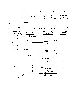
Fig. 1 is a block diagram of a radio pager
15 receiver according to an embodiment of this invention;
Fig. 2 is a time chart for use in describing a
radio call signal received by the pager receiver
illustrated in Fig. l;
Fig. 3 is a diagram for use in describing
20 operation of an RAM which is preferably used in the
pager receiver illustrated in Fig. l;
Fig. 4 is another diagram for use in describing
operation of the RAM mentioned in connection with Fig.
3;
Figs. 5(a) and 5(b) collectively show a flow
chart for use in describing a backup test of the pager
receiver illustrated in Fig. l;
,.
~3~4452
Fig. 6 is another flow chart for use in
describing another backup test of the pager receiver
illustrated in Fig. l; and
Fig. 7 is still another flow chart for use in
5 describing a part of another backup test illustr~ted in
Fig. 6.
Des~ription-of the Preferred Embodiment:
.
Referring to Fig. l, a radio pager receiver 11
according to a preferred embodiment of this invention is
lO operable in response to a radio call signal which is
transmitted ~rom a transmitting station (not shown).
In Fig. Z, the radio call signal is indicated at
RC along a top line. The radio call signal RC comprises
a preamble signal PR of a first predetermined number of
15 bits, a frame synchronization signal FS of a second
predetermined number of bits, a call number signal CN of
a third predetermined number of bits, a message signal
M, and an end signal E of a fourth predetermined number
of bits. The preamble signal PR, the frame
20 synchronization signal FS, the call number signal CN
the message signal M, and the end signal E are
successively arranged to form a frame. In the manner
~shown along a second line labelled PR, the preamble
signal PR is specified by a repetition of pulses which
25 are of logic "l" and "0" levels and are equal in number
to the first predetermined number. The frame
synchronization signal FS has a fixed pattern of the
second predetermined number of bits as shown along a
.
.,
. .
~304L9L5;~
third line labelled FS. The end signal E has another
fixed patt~rn of the fourth predetermined number of bits
as illustrated along a fourth line labelled E. The
fixed pattern of the end signal E is different from the
5 fixed pattern of the frame synchronization signal FS.
Each of the frame synchronization, the end, and the call
number signals FS, E, and CN is formed by a scH
(Bose-Chaudhari-Hocquenghem) code which is well known in
the art.
As depicted in a bottom line labelled "CN or M,"
the call number signal CN comprises an identification
area ID positioned at the most significant bit (MSB)
thereof, an information area INF, and a check bit area
CHK. The call number signal CN is specified by a logic
15 "0" level at the identification area ID and carries, in
the information area INF, a call number which is
assigned to each radio pager receiver. The message
signal M is similar to the call number signal CN, as
shown along the bottom line. The message signal M
20 consists of the BCH code and is specified by a logic "1"
level at the identification area ID. A message is
located in the information area INF of the message
signal M. The message has a variable message length
which is not longer than a preselected maximum length in
25 the manner which will later be described.
Turning back to Fig. 1, the radio pager receiver
11 is for use in combination with a main battery 12 for
generating main electric power and a backup battery 13
,.
~3~4452
for generating backup electric power. The pager
receiver 11 comprises an RAM (random access memory) 14
coupled to the main battery 12 through a manually
operable power source switch 17 and to the battery 13.
5 The RAM 14 is activated by the main electric power when
the switch 17 is closed to an on state. The RAM lA is
backed up by backup electric power when the switch 17 is
opened.
The radio call signal is picked up by an antenna
10 15 and supplied to a receiving portion 16. The
receiving portion 16 is coupled to the main battery 12
through the switch 17 and is activated by the main
electric power when the switch 17 is put into the on
state. The recei~ing portion 16, when activated,
15 converts or demodulates the radio call signal into a
baseband signal carrying the preamble signal PR, the
frame synchronization signal FS, the call number signal
CN, the message signal M, and the end signal E. The
baseband signal is supplied to a decoder 18 as a
20 succession of digital signals.
The decoder 18 is coupled to the main battery 12
through the switch 17. Therefore, the decoder 18 is
activated by the main electric power when the switch 17
is put in the on state. When activated, the decoder 18
25 decodes the baseband signal into the preamble signaI PR,
the frame synchronization signal FS, the call number
signal CN, the message signal M, and the end signal E.
~1.3~4~52
More specifically, the decoder 1~ establishes
bit synchronization with reference to the preamble
signal PR consisting of the repetition of logic "1" and
"0" pulses. Thereafter, the decoder 18 detects the
5 frame synchronization signal FS in order to establish
frame synchroni~ation~
The decoder 18 cooperates with a P-ROM
(programmable read-only memory) 19 so as to detect the
call number signal CN assigned to the pager receiver 11
10 under consideration. More specifically, the P-ROM 19
memorizes a directory number signal of a prescribed
number of bits indicative of a directory number assigned
to the pager receiver 11.
When the frame synchronization is established by
15 detecting the frame synchronization signal FS, the
decoder 18 starts to read the directory number signal
from the P-ROM 19 and compares the call number signal CN
with the directory number signal bit by bit to produce a
coincidence pulse on detection of coincidence between
~0 bits of the call number and the directory number
signals. The coincidence pulse is sent to a message
processor 20 for processing the message signal in the
manner which will presently be described.
The decoder 18 compxises a tone signal generator
25 (not shown) responsive to a drive signal for generating
a tone signal indicative of a call for the pager
receiver in the manner which will presently be
described .
. ' ' ~. .
~;3 0~ 2
The message processor 20 comprises a processing
circuit 21 coupled to the main battery 12 through the
switch 17. The processing circuit 21 is therefore
activated by the main electric power when the switch 17
5 is put in the on state. The processing circuit 21 is
for processing the message signals into the respective
messages and administration data for use in collectively
administrating the messages. The administration data
will later be described. More specifically, the
10 processing circuit 21 processes the message signal into
the message and the administration datum in response to
the coincidence pulse. In this event, the processing
circuit 21 processes the message signals to have the
administration data related to one another in accordance
15 with a logical relationship which will become clear as
the description proceeds.
When processing operation becomes to an end for
each of the message signals, the processing circuit 21
produces a drive signal. In other words, the drive
20 signal is produced when the processing circuit 21
detects the end signal E (Fig. 2). Responsive to the
drive signal, the tone signal generator of the decoder
18 sends the tone signal to a loudspeaker 22 through an
amplifier 23 to make the loudspeaker 22 generate a call
25 tone indicative of arrival of a call to the pager
receiver.
In the manner which will later be illustrated,
the RAM 14 has a message area and an additional area. A
:
'
~L3~)4~5~
12
storing circuit Z4 is activated by the main electric
power like the processing circuit 21. The storing
circuit 24 stores the messages in the message area and
the administration data in the additional area in
5 correspondence to the respective messages in the manner
which will later be described more in detail. At any
rate, the message and the additional areas are used in
memorizing the messages and the administration data as a
content of the RAM 14.
A read control circuit 25 and a backup test
circuit 26 are activated by the main electric power like
the processing circuit 21. The read control circuit 25
will later be described. In the manner which will also
later be described more in detail, the backup test
15 circuit 26 serves as a judging circuit for judging
whether or not the administration data are correctly
kept or retained in the additional area when the R~M 14,
the processing circuit 21, and the storing circuit 24
are activated after once deactivated as a result of
20 manipulation of the switch 17. More specifically, the
backup test circuit 26 judges whether or not the logical
relationship is correctly kept in the additional area.
The backup test circuit 26 thereby produces a result
signal representa~ive of a result of judgement.
An erasing circuit 27 is activated by the main
electric power and is coupled to the backup test circuit
26 and to the RAM 14. When the result signal
representative of the result of judgement indicates that
13044S2
13
the administration data are not correctly kept or
retained in the additional area, the erasing circuit 27
erases the content of the memory 14. For this purpose,
the erasing circuit 27 supplies an earth or ground
S voltage to the RAM 14 during a predetermined time
duration enough to erase the content of th~ memory 14.
The content of the RAM 14 is erased by supplying the
earth voltage to the RAM 14 even while the RAM 14 is put
in the activated state by the main electric power.
Thus, the erasing circuit 27 is coupled to the
backup test circuit 26 and to the message and the
additional areas of the RAM 14 for erasing the messages
and the administration data from the message area and
the additional area in response to the result signal
15 when the result of judgement indicates that the
administration data are not correctly kept or retained
in the additional area.
The message processor 20 may be of a single
semiconductor chip. In this event, the processing, the
20 storing, the read control, and the backup test, and
erasing circuits 21, 24, 25, 26, and 27 may be made
controlled by software.
A display unit 28 is, for example, a liquid
crystal display (LCD). The display unit 28 is connected
25 to tha read control circuit 25 through a display driver
29 in visually displaying the messages and the like.
! Referring to Fig. 3, description will be made as
regards a structure of the RAM 14. It will be presumed
.
.
- .
. :.' , '
- ' ~ .
~IL3~ 52
14
that the RAM 14 is capable of memorizing a maximum of
forty messages and that the RAM 14 is capable of
memorizing messages having a total length equal to
(32 x 56) bytes.
The RAM 14 has a message area 30 and a list area
31 which serves as the additional area and which is used
in memorizing a list of the administration data. The
message area 30 has first through fifty-sixth sectors
which are numbered in Fig. 3 #1 through #56. Each of
10 the sectors has a memory capacity of thirty-two bytes.
As described above, each of the messages has a
variable message length which is not longer than a
preselected maximum length of (16 x 32) bytes. A
predetermined length of thirty-two bytes will be taken
15 into consideration. The messages may include a message
which is longer ~han the predetermined length and will
be called a particular or long message. By the
processing circuit 21 (Fig. 1), the long message is
processed into a succession of message blocks which have
20 the predetermined length in common. The message blocks
are stored in different sectors by the storing circuit
24. The longest one of the messages consists of sixteen
message blocks.
The list area 31 has a first partial area 32 for
25 memorizing a file allocation table labelled FAT as a
portion of the administration data and a second partial
area 33 for memorizing a directory table as a remaining
portion of the administration data. The file allocation
13~L452
table has first through fifty-sixth divisions (later be
illustrated) in one-to one correspondence to the first
through the fifty-sixth sectors of the message area 30.
The directory table has first through fortieth parts
5 (later be illustrated) for memorizing directories in
correspondence to the respective messages memorized in
the message area 30.
Turning to Fig. 4, first through fourth messages
M1, M2, M3, and M4 are memorized in the message area 30.
10 In correspondence, first through fourth parts 35 are
illustrated among first through fortieth parts of the
directory table and are memorized in the second partial
area 33. The fifth through the fortieth parts of the
directory table are similar to the illustrated parts 35.
15 Each of the directories consists of an order pointer 36,
an attribute 37, and a file pointer 38. The attribute
37 and the file pointer 3~ will become clear as the
description proceeds. In the manner which will later be
described more in detail, the order pointers 36 are used
20 in memorizing message linkage information. For each of
the messages memorized in the message area 30, the
message linkage in~ormation is indicative of a message
order in which the message signals are processed by the
processing circuit 21 into the respective messages.
With the file allocation table FAT of the first
partial area 32, twelve divisions 40 are illustrated in
Fig. 4 among the first through the fifty-sixth divisions
- . .
- . :
' ' ' ' ' .
:
~L3~
16
which are in one-to-one correspondence to the first
through the fifty-sixth sectors #l to #56 (Fig. 3).
It will be supposed that the processing circuit
21 (Fig. 1) consecutively processes the message signals
5 M (Fig. 2) into the first through the fourth messages Ml
to M4 and that the storing circuit 24 (Fig. 1)
consecutively stores the first through the fourth
messages Ml to M4 in the message area 30 of the RAM 14.
More particularly, the message signal M carrying the
10 first message Ml is processed at first into the first
message Ml. Therefore, the first message Ml is
memorized at first in the message area 30. Thereafter,
the second message M2 is produced and memorized in the
message area 30. In this manner, the fourth message M4
15 i5 memorized at last in the message area 30 after the
third message M3 is memorized in the message area 30.
In the directory table exemplified in Fig. 4, a
first directory is memorized in the first part 35 in the
manner depicted along a top line. The first directory
20 is for the first message Ml memorized in the message
area 30. The first directory has the order pointer 36
indicating an address of the second part 35 depicted
along a second line. In the second part 35, a second
directory is memorized for the second message M2. The
25 order pointer 36 of the second directory indicates an
address of the third part 35 depicted along a third
line. In the third part 35, a third directory is
memorized for the third message M3. The third directory
~309L452
has the order pointer 36 indicating an address of the
fourth part 35 depicted along a bottom line. A fourth
directory is memorized for the fourth message M4 in the
fourth part 35. The fourth director~ has the order
5 pointer 36 which memorizes a message end mark
representing the fact that the fourth message M4 is last
received by the pager receiver. That is, the message
end mark represents absence of a following message which
may otherwise follow the fourth message M4. The
10 directory table further comprises a list pointer 39
indicating an address of the first part 35 as a start
address of a list of the administration data.
Thus, the order pointers 36 and the list pointer
39 are used in memorizing message linkage information
15 indicative for each of the messages of the message order
in which the message signals are processed into the
respective messages. In this connection, the message
linkage information defines the logical relatio~ship.
It will now be assumed that the first message Ml
20 is a long message mentioned before and that the first
message Ml is processed into first, second, third, and
fourth message blocks. It will also be assumed that the
first through the fourth message blocks are successively
memorized in first through fourth sectors #l to #4
25 (Fig. 3).
Memorized in the first part 35 depicted in the
top line, the first directory has the file pointer 38
indicating an address of the first division 40 of the
.,
~309t~52
18
file allocation table FAT. The first division 40
corresponds to the first sector #l and is indicated or
specified by an arrow extended from the file pointer 3
of the first directory.
The first division 40 has a file pointer
indicating an address of the second division 40 which
corresponds to the second sector #2. The second
division 40 is indicated by an arrow extended from the
file pointer of the first division 40.
The second division 40 has a file pointer
indicating an address of the third division 40
corresponding to the third sector #3. The third
division 40 is specified by an arrow extended from the
file pointer of the second division 40.
The third division 40 has a file pointer
indicating an address of the fourth division 40
corresponding to the fourth sector #4. The fourth
division 40 is indicated by an arrow extended from the
file pointer of the third division 40.
The fourth division 40 memorizes a message block
end mark representing that the fourth message block
memorized in the fourth sector #4 is last received by
the pager receiver among the first through the fourth
message blocks of the first message Ml.
It will readily be understood from a combination
of the part 38 and the divisions 40 for the second
message M2 that the second message M2 is processed into
three message blocks. The third message M3 is not the
~0~52
19
longer message described above. The fourth message M4
is processed into four message blocks.
Thus, the parts 38 of the directory table and
the divisions 40 of the file allocation table FAT are
5 used in memorizing block linkage information indicative
for each of the message blocks of a block order in which
the longer message is processed into the message blocXs.
In other words, the block linkage information defines
the logical relationship.
When the pager receiver newly receives a message
signal carrying a fifth message after reception of the
fourth message M4, the processing circuit 21 (Fig. 1)
processes the message signal into the fifth message. In
this event, the processing circuit 21 produces the fifth
15 message in a form of a succession of message blocks in
the manner described above. The storing circuit 2~
(Fig. 1) stores the message blocks in the respective
empty sectors each of which memorizes no message block.
The storing circuit 24 furthermore stores a fifth
20 direc~ory for the fifth message in an empty part which
memorizes no directory. The empty part is one of the
fifth through fortieth parts of ~he directory table.
The fifth d1rectory has an order pointer which
memorizes a message end mark described before. The
;~ 2~5 fifth directory also has a file pointer indicating an
address of the division which corresponds to a leading
one of the sectors memorizing the message blocks for the
fifth message. Block linkage information for the fifth
52
message is memorized in divisions of the file
allocatioin table F~T like the block linkage information
for each of the first through the fourth messages Ml to
M4.
It should be noted here that the order poin~er
of the fourth directory for the fourth message M4 is
renewed so as to indicate an address of the part
memorizing the fifth directory ins~ead of the message
end mark.
It will be assumed that the pager receiver
receives a message signal carrying a forty-first message
after reception of a fortieth message.
The processing circuit 21 processes the
forty-first message into at least one message block.
15 When the forty-first message is not longer than the
first message Ml, the message processor 20 (Fig. 1)
erases the first message memorized in the first through
the fourth sectors #l to #4 (Fig. 3) to make the first
through the fourth sectors #l to #4 empty. As a result,
20 the first through the fourth sectors #1 to #4 become
empty sectors. The message processor 20 also erases the
first directory and the block linkage information for
the first message Ml.
Thereafter, the storing circuit 24 (Fig. 1)
25 stores at least one message block of the forty-first
message in at least one of the empty sectors. For the
forty-first message, a forty-first directory is
memorized in the first part 35 of the directory table
~L3i~4~L52
21
instead of the first directory for the first message Ml.
Block linkage information for the forty-first directory
is memorized in at least one division of the file
allocation table FAT.
Inasmuch as the first directory is erased, the
list pointer 39 is renewed so as to indicate an address
of the second part 35 which memorizes the second
directory for the second message M2. As a result, a
start address of a list of the administration data
10 ~ecomes the acldress of the second part 35.
When the forty-first message is longer than the
first message Ml and is not longer than a total length
of the first and the second messages Ml and M2, the
message processor 20 may erase the first and the second
15 messages Ml and M2 memorized in the message area 30 so
as to store the forty-first message in the message area
30. In this case, the message processor 20 should erase
the first and the second directories and the block
linkage information for the first and the second
20 messages Ml and M2 in order to renew the directory table
and the file allocation table.
In this manner, the directory table and the file
allocation table FAT are renewed when the forty-first
message is received by the pager receiver.
It should be noted here that the attribute 37 of
each of the directories indicates whether the list is
closed or open in the directory in question. More
specifically, the attribute 37 of the directory in
.
.~,, . . - ,
5~
questlon indicates whether or not renewing operation of
the list becomes an end in the directory in question.
Referring to Figs. 1, 3, and 4, description will
proceed to opera~ion of the read control circuit 25~
5 The pager receiver 11 comprises first and second keys
(not shown) for producing first and second instruction
signals 41 and 42 when the first and the second keys are
operated by a possessor of the pager receiver 11,
respectively. Responsive to the first instruction
10 signal, the read control circuit 25 successively reads
leading message blocks of the messages memorized in the
message area 30 of the R~M 14. The leading message
blocks of the messages are successively sent to the
display driver 29. The display driver 29 makes the
15 display unit 28 successively display the leading message
blocks of the messages. Responsive also to the second
instruction signal, the read control circuit 25
successlvely reads message blocks of one of the messages
memorized in the message area 30 to make the display
20 unit 28 successively display the message blocks of the
message in question.
Turning to Fig. 5, description will proceed to
.
backup test operation of the backup test circuit 26
(Fig. 1).
The backup test circuit 26 comprises a first
working area (not shown) for memorizing flags in
one-to-one correspondence to the respective parts 35
(Plg. 4) of the directory table of the RAM 14 (Fig. 13
l~t)9L~S~
23
Inasmuch as the number of the parts 35 is forty, the
number of the flags is forty. Each of the flags is one
bit and has a logic "1" level.
On starting the backup test operation, the
5 backup test circuit 26 stores the ~lags in the first
working area at a first stage Sl. The first stage Sl is
followed by a second stage S2.
At the second stage S2, the backup test circuit
26 refers to a content of the list pointer 39 (Fig. 4).
10 The second stage S2 is followed by a third stage S3. At
the third stage S3, judgement is carried out whether or
not the content of the list pointer 39 is an end mark.
When a result of the judgement is affirmative, operation
proceeds to a fourth stage S4 which will later he
15 described. In this case, no message is memorized in the
message area 30 (Fig. 4). When the result of the
judgement is negative, operation proceeds to a fifth
stage S5. In this ca9e, the content of the list pointer
39 indicates an address of a directory for a leading
20 message as described above. At the fifth stage S5,
judgement is carried out whether or not the address of
the directory for the leading message is an illegal
address. The illegal address specifies an undeflned
address other than addresses which are present within
25 the directory table. When a result of the judgement is
affirmative, the fifth stage S5 is followed ~y a sixth
stage S6. Otherwise, the fifth stage is followed by a
seventh stage S7.
:
, . . .
~13al~S2
24
At the sixth stage S6, the backup test circuit
26 makes the erasing circuit 27 erase the content of the
RAM 14 (Fig. 1) because the memory backup operation ends
in failure.
At the seventh stage S7, judgement is made
whether or not the address of the directory for the
leading message erroneously indicates a forty-first
directory which is undefined. When a result of the
judgement is affirmative, operation proceeds to the
10 sixth stage S6. Otherwise, operation proceeds to an
eighth stage S8.
At the eighth stage S8, judgement is made
whether or not the list is closed with reference to the
attribute 37 (Fig. 4) of the directory in question.
15 When a result of the judgement is negative, operation
proceeds to a ninth stage S9 which will later be
described. Otherwise, operation proceeds to a tenth
stage S10.
At the tenth stage S10, judgement is carried out
20 whether or not the flag corresponding to the directory
in question is still a logic "1" level. When the flag
is not a logic "1" level, the memory backup operation is
a failure. Operation therefore proceeds to the sixth
stage S6. Otherwise, operation proceeds to an eleventh
25 stage Sll at which the flag is erased from the first
working area. As a result, check operation becomes to
an end for the directory of the leading message. The
eleventh stage Sll is followed by a twelfth stage S12.
:
,
4~;2
At the twelfth stage S12, the backup test
circuit 26 refers to an order pointer of the directory
for the leading message. The twelfth stage S12 is
followed by the third stage S3.
Check operation is made for a next directory
having an address which is indicated by the order
pointer of the directory for the leading message. Such
check operation is made in the manner similar to the
check operation for the directory of the leading message
10 at the third, the fifth, the seventh, the eighth, and
the tenth stages S3, S5, S7, S8, and S10.
When the next directory has an order pointer 36
which memorizes an end mark (that is, a message end
mark), the third stage S3 is followed by the fourth
15 stage S4.
At the fourth stage S4, the backup test circuit
26 carries out erasure operation of unchecked
directories. The fourth stage S4 is followed by a
thirteenth stage S13 which will later be described.
When the next directory has an attribute 37
indicating that the list is open, the eighth sta~e S8 is
followed by the ninth stage S9.
At the ninth stage S9, the backup circuit 26
stores a message end mark in the order pointer of the
25 directory for the leading message. In other words, the
message end mark is stored in the order pointer of a
previous directory which is stored immediately before
.. . . .
~L3~4~52
26
the next directory. In this manner, the list is closed.
The ninth stage S9 is followed by the fourth stage S4.
A last directory corresponding to a last message
has an order pointer having a message end mark. When
5 check operation becomes to an end for the last
directory, the message end mark is detected at the third
stage S3. ~s a result, operation proceeds to the ~ourth
stage S4 which is followed by the thirteenth stage 513.
Thus, the backup test circuit 26 judges whether
10 or not the message linkage information is correctly kept
or retained in the additional area 33. That is, the
backup test circuit 26 judges whether or not a logical
relationship of the message linkage information is
correctly kept in the additional area 33.
Description will proceed to check operation of
the block linkage information.
The backup test circuit 26 further comprises a
second working area (not shown) for memorizing flags in
one-to-one correspondence to the respective divisions 40
20 (Fig. 4) of the file allocation table FAT (Fig. 4) of
the RAM 14. The divisions 40 are in one-to-one
correspondence to the sectors #l to #56 of the message
area 30 as described above. Inasmuch as the number of
the diyisions 40 is fifty-six, the number of the flags
25 is fifty-six. Each of the flag is one bit and has a
loqic "1" level.
At the thirteenth stage S13, the backup test
circuit 26 stores the flags in the second working area.
, .
- - i
130~5Z
The thirteenth stage S13 is followed by a fourteenth
stage S14.
At the fourteenth stage S14, the backup test
circuit 26 again refers to a content of the list pointer
5 39. The fourteenth stage S14 is followed by a fifteenth
stage S15.
At the fifteenth stage S15, judgement is carried
out whether or not the content of the list pointer is an
end mark. When a result of the judgement is
10 affirmative, operation proceeds to a sixteenth stage S16
which will later be described. When the result of the
judgement is negative, operation proceeds to a
seventeenth stage S17. In this case, the content of the
list pointer 39 indicates an address of a directory for
15 a leading message as described above.
At the seventeenth stage S17, the backup test
circuit 26 refers to a file pointer 38 (Fig. 4) of the
directory for the leading message. The file pointer 38
of the directory for the leading message indicates an
20 address of a division 40 corresponding to a sector which
memorizes a first message block of the leading message.
The seventeenth stage S17 is followed by an eighteenth
stage S18.
At the eighteenth stage S18, judgement is
25 carried out whether or not a content of the file pointer
38 is a message block end mark. When a result of
judgement is affirmative, operation proceeds to a
nineteenth stage Sl9 which will later be described.
~ , ~
28
When the result of the judgement is negative, operation
proceeds to a twentieth stage S20.
At the twentieth stage S20, judgement is carried
out whether or not the address indicated by the file
5 pointer 38 of the directory for the leading message is
an illegal address other than addresses which are within
the file allocation table FAT. When a result of the
judgement is affirmative, operation proceeds to the
sixth stage S6 described above. When the result of the
10 judgement is negative, operation proceeds to a
twenty-first stage S21.
~ t the twenty-first stage S21, judgement is made
whether or not a division 40 having the address
indicated by the file pointer 38 of the directory for
15 the leading message corresponds to a sector which is
used in memorizing one of first through sixteenth
message blocks for each message. A seventeenth message
block does not have to appear in such judgement~ This
is because a message of seventeen message blocks is
20 undefined in this pager receiver. When the result of
the judgement is negative, operation proceeds to the
sixth stage S6 described above. When the result of the
judgement is affirmative, operation proceeds to a
twenty-second stage S22.
as At the twenty-second stage S22, judgement is
carried out whether or not the flag corresponding to the
directory in question is still a logic "1" level. When
the flag is not a logic "1" level, operation proceeds to
.
:
13(~ 2
~9
the sixth stage S6. Otherwise, operation proceeds to a
twenty-third stage 23 at which the flag is erased from
the second working area. As a result, check operation
becomes to an end for the file pointer 38 of the
5 directory for the leading message. The twenty-third
stage S23 is followed by a twenty-fourth stage S240
At the twenty-fourth stage S24, the backup test
circuit 26 searches for a second division 40 located in
the address which is indicated by the file pointer 38 of
10 the directory for the leading message. The second
division 40 has a file pointer indicating either a
message block end mark or an address of a different
division 40 corresponding to a sector which memorizes a
second message block of the leading message.
When the message block end mark is detected at
the eighteenth stage S18, operation proceeds to the
nineteen~h stage Sl9. Otherwise, operation proceeds to
the twelfth stage S20 described above.
At the nineteenth stage Sl9, the backup test
20 circuit 26 refers to an order pointer of the directory
for the leading message.
Check operation of the block linkage information
is made for a next directory having an address which is
indicated by the order pointer of the directory for the
25 leading message. Such check operation is made in the
manner similar to the check operation of the block
linkage information for the directory of the leading
message at the fifteenth, the seventeenth, the
~3~4~52
eighteenth, the twentieth, the twenty-first, the
twenty-second, the twenty-third, and the twenty-fourth
stages S15, S17, S18, S20, S21, S22, S23, and S24.
When the next directory has an order pointer 36
5 which memoriæes an end mark (that is, a message end
mark), the fifteenth stage S15 is followed by the
sixteenth stage S16.
At the sixteenth stage S16, the backup test
circuit 26 carries out erasure operation of unchecked
10 divisions. The sixteenth stage is followed by a
twenty-fifth stage at which the backup test circuit 26
confirms that the memory backup is correctly carried
out.
Thus, a last directory corresponding to a last
15 message has an order pointer having a message end mark.
. When check operation of the block linkage information
becomes to an end for the last directory, the message
end mark iB detected at the fifteenth stage S15. As a
result, operation proceeds to the sixteenth stage S16
20 which is followed by the twenty-fith stage S25.
As described above, the backup test circuit 26
judges whether or not-the message linkage information is
correctly kept or retained in the additional area 33.
That is, the backup test circuit 26 judges whether or
25 no~ a logical relationship of the block linkage
~: information is correctly kept in the additional area 33.
~3~52
31
Referring to Figs. 6 and 7, description will
proceed to another backup test operation of the backup
test circuit 26 (Fig. 1).
Referring to Fig. 6, a twenty-sixth stage S26 is
5 carried out instead of the fourth stage S4 illustrated
in Fig. 5. When the result of the judgement at the
third stage S3 is affirmative, the third stage S3
proceeds to the twenty-sixth stage S26. The
twenty-sixth stage S26 also follows the ninth stage S9.
10 At the twenty-sixth stage S26, judgement is made whether
or not an unchecked directory is present. The unchecked
directory is, or example, an independent directory
having an administration datum which is not related at
all to other administration data in accordance with a
15 logical relationship. When the unchecked directory is
present, operation proceeds to the sixth stage S6 at
which ~he content of the RAM 14 is erased. otherwise,
the twenty-sixth stage S26 is followed by the thirteenth
stage S13.
Referring to Fig. 7, a twenty-seventh stage S27
is carried out instead of the sixteenth stage S16
illustrated in Fig. 5. When the result of the judgement
at the fifteenth stage S15 is affirmative, the fifteenth
stage S15 proceeds to the twenty-seventh stage S27 at
25 which an unchecked division 40 is present. The
unchecked division 40 (Fig. 4) is, for example, an
independent division having an administration datum
which is not related at all to other administration data
.~
~3134~52
in accordance with a logical relationship. When the
unchecked division is present, operation proceeds to the
sixth stage at which the content of the RAM 14 is
erased. Otherwise, the twenty-seventh stage S27 is
5 followed by the twenty-fifth stage S25 described above.
- : ' .
.
: ' - '' '