Note : Les descriptions sont présentées dans la langue officielle dans laquelle elles ont été soumises.
1 3 ~ 4
5 e ~ q ~
Apparatus for fabricatin~ semiconductor dcv~
The present invention relates generally to an
apparatus for fabricating a semiconductor device and, more
particularly, to an apparatus for individually separating
semiconductor chips formed on a semiconductor wafer.
A technique for individually separating a plurality of
chips formed on a single wafer i8 called "dicing~. As a
separating method, there are two systems; a scribing
system in which the wafer is scribed along the chips to
form scribed grooves, using a laser or a diamond needle,
with the chips being subsequently mechanically separated,
and a dicing saw system in which the high speed rotation
of a thin diamond blade is used to cut deep into the wafer
so that the chips can be readily mechanically separated or
become separated during the cutting.
To enable the prior art to be described with the aid
of a diagram, the figures of the drawings will first be
listed
Fig. l is a schematic side view of an apparatus for
fabricating a semiconductor device according to a first
preferred embodiment of the present invention;
Figs. 2(a) and 2(b) are fragmentary sectional views
showing how a wafer deforms when pressed by a pressing
means;
*
3 ~ ~
-- 2 --
Figs. 3 and 4 are schematic side views of apparatus
according to second and third embodiments of the present
invention; and
Fig. 5 is a schematic side view of a prior art
S apparatus.
A wafer half-cut with either the scribing technique or
the dicing technique involves dividing the wafer into
individual chips by mechanical means.
Fig. 5 illustrates schematically one prior art
apparatus for dividing the wafer. This apparatus comprises
a base 1 with a rubber mat 2 thereon. A half-cut wafer 3
having first and second surfaces opposite to each other
and having chips formed on its first surface is placed on
the rubber mat 2, with its first surface confronting the
rubber mat 2 and its second surface facing upwardly. Prior
to the placement of the wafer 3 on the rubber mat 2, an
adhesive tape 5 is applied to the second surface of the
wafer so that, when the wafer 3 is divided, the chips will
not scatter and are retained in position.
A peripheral surface of a generally cylindrical roller
14 is pressed against the second surface of the wafer 3,
and the roller is driven to rotate about its longitudinal
axis to divide the wafer 3. The chips divided from the
wafer remain separated on the tape 5 which is suitably cut
according to need.
This prior art apparatus is so designed that the wafer
supported by the elastic rubber mat is divided when the
roller is pressed against it. Both the wafer and the
rubber mat are deformed downwardly when pressed by the
roller. Because of this, the wafer can only be divided in
one direction. In order for a wafer that has been scribed
to be divided in both the X-axis and the Y-axis, the
process must be repeated.
Moreover, while the pressing surface exhibited by the
- 3 ~
ro~ation of the roller is flat, a peripheral area of the
wafer may have a film, such as a SiN film, left unremoved,
rendering the peripheral area of the wafer thicker than
the remainder thereof. To avoid this problem, a greater
5 pressing force may be exerted on the peripheral area of
the wafer than on a central area thereof.
Furthermore, according to the prior art apparatus,
localized areas of the wafer tend to be excessively
pressed, which can result in breakage of the wafer and/or
10 damage to the wiring fabricated on the wafer. In order to
avoid these problems, an adjustment of the pressing force
is required, rendering the apparatus expensive. In
addition, subsequent to the separation of the chips from
the wafer, the adhesive tape must be expanded to separate
15 the chips individually, and this requires additional
manufacturing steps.
The present invention has been devised with a view to
substantially eliminating the above described problems
inherent in the prior art apparatus, and has for its
20 essential object to provide an improved apparatus for
fabricating a semiconductor device, which is effective to
accurately separate the chips in a single process without
excessive pressing force being applied.
In order to accomplish this object the invention
25 provides an apparatus for fabricating a semiconductor
device by individually separating semiconductor chips
formed on a wafer, which comprises a flexible mat: means
for supporting the mat in a substantially horizontal
position; a pressing means having a generally convex body
30 and being supported for movement up and down; and a drive
means for vertically moving the pressing means and the
wafer relative to one another, said wafer having first and
second surfaces opposite each other with chips formed on
the first surface thereof, said wafer being placed on the
mat with the chips confronting the mat, and said convex
boc3y of the pressing means being pressed against the second
surface of the wafer to separate the chips on the wafer.
Preferably, the flexible mat will be circular in shape
and made of rubber.
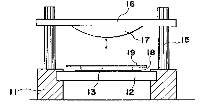
Referring first to Fig. 1, the apparatus comprises a
generally annular base 11 having a generally circular
rubber mat 12 mounted thereon so as to close the opening
of the base 11. At least three, preferably four, upright
posts 15 are rigidly mounted to extend upwardly from the
base 12, these posts being equally spaced apart in the
circumferential direction of the base 12. The upright
posts 15 carry a generally circular, horizontal pressing
plate 16 that can move towards and away from the mat 12
along the posts 15. The pressing plate 16 has one surface
formed with a domed body 17 protruding downwardly towards
the mat 12. A drive mechanism for moving the plate 16
towards and away from the mat 12 is not illustrated, and
can be of any known construction.
When this apparatus is to be operated, a wafer 13
having first and second surfaces opposite each other and
with chips formed on its first surface is placed on the
mat 12 above a surface protective tape 18. During this
placement, care must be taken that the wafer 13 is placed
on the mat 12 with the chips on its first surface in
contact with the tape 18 and with its second surface
facing upwards. The second surface of the wafer 13 has a
tape 19 applied thereto so that, when the wafer 13 is
placed on the mat 12 in the manner just described, the
tape 19 on the second surface of the wafer 12 faces
upwards and away from the mat 12.
After such placement of the wafer 13, the drive
mechanism is operated to move the pressing plate 16 down-
wards towards the wafer 13 on the mat 12. As a result,
9 3 ~3 ~
-- 5 --
the body 17 on the plate 16 is brought into contact with
the wafer 13 through the tape 19, substantially as shown
in Fig. 2(a). When the body 17 is brought into full
contact with the wafer 13 as the plate 16 is moved further
5 downwards, the wafer 13 together with the mat 12 is
deformed downwardly to follow the curvature of the body
17, as shown in Fig. 2(b). While the wafer 13 is being so
deformed together with the mat 12, cracking is initiated
in the wafer 13 starting from a central area thereof and
10 extending towards its periphery. However, the force
applied by the body 17 on the wafer 13 no longer acts on
the wafer once the cracking takes place to separate the
chips individually.
Accordingly, even though the wafer has a greater
15 thickness at its peripheral area than at its central area,
because of the presence of a film such as a SiN film, the
chips formed on the wafer 13 receive a uniform pressing
force transmitted from the body 17. The application of
the force uniformly over the chips on the wafer 13 results
20 not only in minimization of any possible damage to the
chips, but also in the separation of the chips in both the
x-axis and the y-axis.
In a second preferred embodiment shown in Fig. 3, the
apparatus comprises a base 21 having at least three,
25 preferably four, upright posts 25 secured thereto to
extend upwards, and a generally circular, horizontal
rubber mat 12 mounted thereon by an annular member, for
movement towards and away from the base 21 along the posts
25. The annular member supporting the mat 12 also
supports a tape 28 on which the wafer 13 is placed
immediately beneath the mat 12.
The apparatus also comprises a pressing block 26
rigidly mounted on the base 21 and having a generally
domed body 17 integrally formed therewith to protrude
~c ~ t~
upwardly. A wafer ring 29 surrounds the body 17, being
supported on a plurality of posts for movement up and
down. The body 17 has a heater embedded in it for heating
the body 17 to a predetermined temperature, for example,
S about 60C.
When this apparatus is operated, the wafer 13 is
placed on the tape 18 with the chips on the first surface
thereof confronting the mat 12. The drive mechanism is
then operated to move the wafer 13 together with the mat
10 12 and the tape 28 downwardly towards and into contact
with the body 17, thereby deforming the wafer 13 and the
mat 12 to follow the curvature of the body 17. It is to
be noted that, shortly before the wafer 13 is deformed by
contact with the body 17, the latter comes into contact
15 with the tape 28 and that the tape 28 is heated thereby,
which enhances its ductility.
When the wafer 13 is so deformed with the mat 12,
cracking is initiated in the central area of the wafer 13
and extends towards its periphery. However, the pressing
20 force applied by the body 17 to the wafer no longer acts
on the wafer once the cracking has taken place to separate
the chips individually.
After the cracking has occurred in the wafer 13, the
mat 12 is, together with the wafer 13, moved a further
25 predetermined distance downwards to allow the tape 28 to
elongate or expand while separating the chips
individually. Thereafter, the wafer ring 29 is shifted
upwardly by a suitable drive mechanism to urge the tape
28, which has previously been expanded thereover, against
30 the wafer 13 from below.
From the foregoing description it will be clear that
with this apparatus, not only can the chips on the wafer
be individually separated, but the application of tape to
the wafer can also be accomplished, thus minimizing the
35 number of manufacturing steps.
L ~
Referring now to Fig. 4, the apparatus shown therein
is generally similar to that shown in and described with
reEerence to Fig. 1. However, the apparatus of Fig. 4 has
a wafer ring 29 corresponding in function to the wafer
5 ring 29 of Fig. 3 for automatically applying a tape to the
wafer 13. For this purpose, the apparatus of Fig. 4 is
provided not only with the wafer ring 29, but also with a
support ring vertically slidably mounted on the upright
posts 15 and having a tape 38 stretched across it to lie
10 immediately below the domed body 17. The wafer ring 29 in
the apparatus of Fig. 4 is supported by a plurality of
rods that can slide through the presser plate 16 for
vertical movement independently of the movement of the
plate 16. These rods are coupled to a drive mechanism
lS tnot shown).
The apparatus of Fig. 4 operates in the following
manner.
The wafer 33 having chips on its first surface is
placed on the mat 12 with the chips in contact with the
20 mat 12. The drive mechanism is then operated to move the
plate 16 downwards towards the wafer 33.
During this downward movement of the plate 16, the
body 17, which is heated to about 60C, comes into contact
with the tape 38 to enhance the ductility of this tape.
25 The plate 16 is then moved further downwards until the
domed body 17 is brought into contact with the wafer 33 on
the mat 12. Upon further such downward movement, the
wafer 33 and the mat 12 are downwardly deformed, i.e.,
made concave to follow the curvature of the body 17.
30 Cracking is initiated in the central area of the wafer 33
and extends towards its periphery. However, the pressing
force applied by the body 17 to the wafer no longer acts
on the wafer once the cracking takes place to separate the
chips individually.
a ~1
After this cracking occurring in the wafer, the wafer
rirg 29 is lowered to retain the tape 38 pressed against
the mat 12. When the pressing plate 16 is again elevated,
the tape 38 is expanded by the wafer ring 29 and applied
5 to the wafer 33. Thereafter, the wafer ring 29 is shifted
upwardly in readiness for removal of the separated chips
now retained by the tape 38.
Although the present invention has been fully
described in connection with the preferred embodiments
10 thereof with reference to the accompanying drawings, it is
to be noted that various changes and modifications are
apparent to those skilled in the art. Such changes and
mod~fications are to be understood as included within the
scope of the present invention unless they depart
15 therefrom.