Note : Les descriptions sont présentées dans la langue officielle dans laquelle elles ont été soumises.
1312387
The present invention relates to a hybrid printed
circuit board used, for exampl~, in a PBX (Private Branch
Exchange).
The PBX accommodates a lot of circuit boards
respectively including circuits for interfacing with a
terminal, such as a telephone. Commonly, one PBX
accommodates as many as 50 boards, including 8 to 16 sets of
interface circuits thereon. The accommodating form of these
boards is like "accommodating books (printed boards~ in a
bookcase (PBX~". This means that the area and the thickness
of a printed circuit board have a great effect on the size of
PBX.
Accordingly, in a PBX system which requires a lot of
printed circuit boards, the area of a printed circuit board
has a great effect on the size of PBX. Heretofore, a
technique has been well known for mounting a particular type
of printed circuit board, which is referred to as a "hybrid
printed circuit board". This board is constructed by
electrically connecting a plurality of circuit devices on the
board through leads. This means that the hybrid printed
circuit board requires disposing a plurality of circuit
devices in a predetermined space. Thus, if the area of the
board is reduced, this results in a reduction of the size of
.
-- 1 --
i ~,
131~387
the PBX system.
Yet, the hybrid conventional printed circuit board
generally requires more space than printed circuit boards.
Thus, miniaturization of a PBX system in which hybrid printed
boards are used becomes difficult.
In one aspect, the present invention provides a hybrid
circuit board for mounting on a main circuit board, the
hybrid circuit board comprising: a flat circuit board having
two first long sides, two first short sides, a first
thickness, a first upper surface, and a plurality of first
leads, the flat circuit board having a first lead-disposed
area along the first long sides of the first upper surface of
the flat circuit board~ the first leads being disposed at
intervals in the flat lead-disposed area, the flat circuit
board having at least two first lead-free areas along both
first long sides of the first upper surface, the first leads
not being disposed in the first lead-free areas; and at least
one flat circuit device having two second long sides, two
second short sides which are shorter than the first short
sides, a second thickness, a second upper surface and second
leads at intervals along both second long sides of the second
- 2 -
1312387
upper surface, the second leads being disposed in the first
lead-free area of the flat circuit board.
Fig. 1 is a view showing an outer appearance of a PBX
employing a hybrid printed circuit board of this invention;
Fig. 2 is a block diagram for explaining an arrangement
of a subscriber's circuit;
Fig. 3 is a block diagram for explaining arrangement of
the first subscriber's circuit of Fig. 2;
Fig. 4 is a perspective view of a printed board having a
subscriber's circuit;
Fig. 5 is a plan view showing a hybrid printed circuit
board of this invention;
Fig. 6 is a longitu*oinal section showing a hybrid
printed circuit board of this invention;
Fig. 7 is a view showing two neighboring printed boards
of the PBX shown in Fig l; and
Fig. 8 is a perspective view showing a hybrid printed
circuit board of the second embodiment and another printed
board for mounting this hybrid printed circuit board thereon.
Hereinafter, embodiments of this invention will be
described.
; 25 Fig. 1 is a view showing an outer appearance of a PBX
employing a hybrid printed board of this invention.
- 3 -
1 3 1 2387
PBX 102 shown in Fig. 1 accommodates about 70 printed
boards 104 in a manner resembling the stacking of books in a
bookcase. Each printed board 104 includes about 16
subscriber's circuits.
Fig. 2 is a block diagram for explaining the arrangement
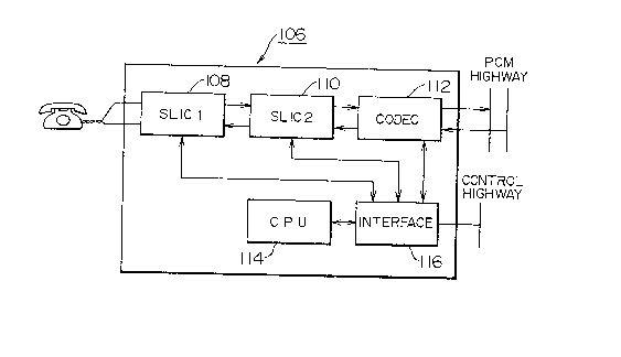
of such a subscriber's circuit.
The subscriber's circuit 106 shown in Fig. 2 is disposed
between a PCM highway and a control highway conducting from
the circuit of a digital system and a terminal machine, such
as a telephone. This subscriber's circuit 106 is composed of
a first subscriber's circuit 108 in charge of ring back tone
control and test control, a second subscriber's circuit 110
in charge of power feed control, overvoltage protection,
; 15 circuit monitor and 2/4 line conversion, a codec circuit 112
for converting a digital signal from the PCM highway into an
analogue signal and an analogue signal supplied to the PCM
highway into a digital signal, a CPU 114 for integrally
controlling the subscriber's circuit 106 and an interface
circuit 116 for interfacing these respective circuits to a
control highway.
Fig. 3 is a block diagram for explaining an arrang~ment
of the first subscriber's circuit 108.
- 4 -
1312387
The first subscriber's circuit 108 shown in Fig. 3 is
composed of four FET switches 118, 120, 122, 124 for various
kinds of switching, a control circuit 126 for controlling
each switching and photocouplers 128 to 134 laid between
these FET switches and the control circuit~
Fig. 4 is a perspective view showing a printed board 104
provided with such a subscriber's circuit 106 as described
above.
The printed board 104 shown in Fig. 4 is composed of a
subscriber's circuit area 136 having subscriber's circuits
106 and a control circuit area 138 having control circuits
for controlling these subscriber's circuits 106.
The subscriber's circuit area 136 includes first subscriberrs
circuits 108 ~or respective subscriber's circuits, second
subscriber's circuits 110 and codec circuits 112 along the
direction of an arrow shown in this figure. The subscriber's
circuits 106 of the abovementioned circuits are ~ormed on a
hybrid printed circuit board 140.
Fig. 5 is a plan view showing such a hybrid printed
circuit board 140 and Fig. 6 is a longitudinal section
showing the board 140.
- 5 -
1 3 1 2387
The hybrid printed circuit board shown in these Figures
is composed of FET switches 118 to 124, a control circuit 126
and photo couplers 128 to 134 formed on the printed board
142.
The printed board 142 typically is 11 mm in height and
90 mm in.width. There is disposed on the lead-disposed area
along one of the longer sides of the printed board 142 thirty
pads 144 for lead connection that are respectively 2 mm is
height and 1 mm in width. This longer side includes about 21
mm-long area in the center thereof which is assigned as a
lead-free area 146 on which leads are not disposed. Thus, in
this area no pad 144 is provided.
The control circuit 126, serving as the circuit device, is
10.5 mm in height and 19 mm in width and is disposed
substantially near the center of the printed board 142. The
control circuit 126 has second leads 147. The second leads
147 of the control circuit 126 are positioned near the lead-
free area 146. The ~ontrol circuit 126 is spaced from the
pads 144 by about 1 mm. The control circuit 126 contains two
; FET switches and photocouplers formed on both sides thereof.
These FET switches
~: :
- 5a -
6 13123~7
and photocouplers are respectively smaller than the control
circuit in height and width.
Each pad 144 has a lead 148 for connecting with the
printed board 104. The lead 148 is about 4.6 mm in length.
Fig. 7 is a view showing two neighboring printed boards
104 of those boards shown in Fig. 1.
As shown in Fig. 7, the lead 148 projected on the
hybrid printed board 104 is fixed by soldering through a
through hole 150 provided in the printed board 104.
The lead 148 projected through the through hole 150 to
the rear side is 2 mm in length, the hydrid printed circuit
board 104 is 12 mm in height from the printed board 104
surface (including 1 mm lead length~, the interval between
the top of the lead 148 and the top of the hybrid printed
circuit board 104 is 2 mm and the printed board is 1.6 mm
in thickness. This means that the interval between the
neighboring printed boards 104 is about 20 mm.
The provision of the lead-free area 146 results in an
interval between the printed boards 104 which is as small as
about 20 mm, as described above. If the leads 148 are
disposed on the area corresponding to the lead-free area
146, the printed board 142 in the hybrid printed circuit
board is about 15 mm in height on the basis of the fact that
the control circuit 126 is 10.5 mm in height, the pad 144 is
2 mm in height and the gap between the control circuit 126
and the pad 144 is about 2 mm in height and the gap between
the control circuit 126 and the pad 144 is about 2 mmO
Thus, the printed board 142 to which this invention is
1 3 t 23~7
applied is lower than the normal printed board by about
4 mm. One rack in the P~3X shown in Fig. 1 accommodates
fourteen printed boards 104, so that he width of the PBX 102
is made shorter by about 50 mm.
Furthermore, this embodiment forms the control circuit
126 substantially near center of the printed board 142, so
that the wiring design of the hybrid printed circuit board
140 is facilitated and miniaturized, because the control
circuit 126 includes the largest number of input and output
pins among the cells loaded on the hybrid printed circuit
board 140. Thus, if this control circuit 126 is located in
the center of the printed board 142, allowance for design is
guaranteed and the inner layers of the printed board 142 are
reduced in number.
Moreover, due to provision of the lead-free area 146,
this embodiment allows wiring patterns to be provided on the
surface of the printed board 104 under the lead-free area
146. Thus, it is possible to guarantee allowance for design
of the printed board 104 employing the hybrid printed
circuit board 140.
Fig. 8 is a perspective view showing a printed board on
which the hybrid printed circuit board of the second embodiment
is mounted.
~f~ The hybrid printed circuit board ~ shown in this
figure is composed of a control circuit 156, FET switches
(not shown) and photo couplers ~not shown) formed on a
printed board 152.
The printed board 154 is 67 mm in length and 12.5 mm in
1312387
width. Each longer side of thls printed board 154 contain
15 pads for lead connections disposed thereon, that are
respectively 2 mm in length and 1 mm in width. The 21 mm-
long areas in the centers of the longer sides are assigned
as lead-free areas. Thus, in this area no pads 158 ~ f~Re
provided.
The control circuit 156 is 10.5 mm in length and 19 mm
in width and is formed substantially near the center of the
printed board 154. Thus, the control circuit 156 includes
the portions positioned in the lead-free areas 160, 162.
The control circuit 156 is spaced from the pad 158 by about
1 mm. The control circuit 156 contains two FET switches and
photocouplers formed on each side. These FET switches and
photocouplers are smaller than the control circuit in width
and height.
w ~ th
Each pad 158 has a lead 166 for connecting ~
printed board 164, that is formed perpendicularly. This
means that this hybrid printed circuit board 152 is disposed
in parallel with the printed board 164.
This embodiment has a reduced width of the hybrid
printed circuit board 152, resulting in reduction of the
width of the printed board 164 employing this hybrid printed
circuit board 152.
Further, like the first one, this embodiment
contributes to facilitating and simplifying wiring design of
the hybrid printed board circuit 152 and reducing the
pattern size and guarantees allowance for design of the
printed board 164 employing the hybrid printed board 152.
9 1 3 1 2387
Heretofore, this invention has been described with
reference to the embodiments, but, this invention is not
limited to these embodiments and can be modified in many
ways without departing from the spirit of this invention.
::~