Note : Les descriptions sont présentées dans la langue officielle dans laquelle elles ont été soumises.
200GZ80
D-8~-1-235 -1- PATENT
ELECTRONIC ~ALLAST CIRCUIT FOR DISCHARGE LAMP
FIELD OF THE INVENTION
The present inventîon relates in general to
ballast circuits for lamps, and pertains, more
particularly, to electronic ballast circuits,
particularly for use with electric discharge lamps~
~ACRGROU~D OF THE INVENT ION
One conventional electronic ballast circuit is one
that employs an inductive ~allast, typically dropping
about 80% of the line voltage arross the ballast
element. There are many applications in which such an
in~uctive ballast are effective. However, for in
particular, low voltage, hiqh current electric
discharge lamps, such as negative glow lamps, an
inductive ballast is highly inefficient. For example,
20 in the particular case of a 15 volt high current
negative glow lamp, undesirably substantially all of
the RMS line voltage would be dropped across the
ballast element.
Accordingly, the use of an inductive ballast for
this type of lamp for a low voltage high current
discharge lamp result~ in poor lamp efficiency.
Because of the relatively high currents required by
these lamps, the corresponding Joule heating loss
~I R, eddy current, hysteresis, etc.) are much
higher than for a lamp operating at lower currents.
In this regard, the higher current referred to would
be in the range of 2-5 amps and the lower currents
-, : ' : , . . ..
~6X~tt~
D-83-1~235 -2- PATENT
would be less than one amp. Accordingly, it is
desirable because of these poor efficiencies
associated with inductive ballasts to instead provide
a more efficient ballast circuit, particularly for use
Fit with di~charge lamps inclu~inq DC glow discharge lamps.
Prior U.S. patents that describe the use of
capacitive ballasts with or without rectifier circuits
lnclude U.S. Patent No. 2,356,369 to Abernathy: U.S.
Patent No. 4,288,725 to Morton; U.S. Patent No.
4,172,981 to Smith; U.S. Patent No. 4,500,812 to
Roche; and U.S. Patent No. 3,787,751 to ~arrow.
Modifications to inductive ballasts have been carried
out. For example, indictive ballasts can be designed
so that resistive and magnetic power losse~ are
lS minimized. However, to minimize both the ballast
weight and system power losse~, a capacitive ballast
is pref~rred, particularly for negative glow, low
pressure discharge lamps, a capacitive ballast in
conjunction with a bridge rectifier has been employed
in the prior art. In this regard, refer to, for
e~ample, the article ~Capacitor ~allast for a Compact
Fluorescent Lamp" by Watanabe, J. Light ~ ~is. Env.,
Vol. 7, ~o. 1, 1983, pp. 7-14. In this article, refer
in particular to the circuit of FIG. 17 employin~ the
combination of a bridge rectifier and capacitor
ballast.
Reference is also made herein to FIG. 1 for an
illustration of the use of a capacitor ballast in
conjunction with a full-wave rectifier bridge for
operating a low voltage, high current DC discharge
lamp. More particularly, FIG, 1 illustrates thP
ballast element as capacitor C. The full wave
D-88-1~235 -3- PATENT
rectif ier bri~e ~fi compri~;0d of diod~s Dl-D4
interconnected in the normal bridge rectif ier
configuration. The input AC ~ignal which typically is
a 120 volt AC ~ignal i6 coupl~d at the terminals 10.
The te~minals 10 connect in series with the capacitor
C to the input of the full-wave rectifier bridge. Th~
output of the full-wave rectifier bridge may be
considered as coupling to the glow discharge lamp 12.
j The glow discharge lamp 12 is comprised of an
anode 14 and a cathode 16. Also illustrated in FIG. 1
is the switch 20. The switch 20 couples, in one
: position thereof, across the cathode 16. The
operation of the switch 20 is well known and as the
construction thereof forms no part of the present
invention, it is not dsscribed in any great detail
herein. It is efficient to stat~ that the switch 20
' is operable for lamp starting. Refer, for e~ample, to
i similar starting switch configurations found in U.S.
Patent No. 2,356,369 or U.S. Patent No. 4,288,725
previously referred to.
One of the drawbacks associated with the
electronic ballast circuit of FIG. 1 is the
characteristic of the circuît of operating with a
single hot spot operation regime for the lamp
cathode. This is illustrated by the arrows 18 in FIG.
1. In essence, the discharge current flows to the
i same point on the cathode, as illustrated hy arrows
¦ lS, during eac~ half cycle o~ the ~C signal.
2~)136:~0
D-a8-1 235 -9- PATENT
~UMMARY OF THE INVEMTION
Accordingly, it is an object of the present
invention to pro~ide an improved electronic ballast
circuit, particularly an electronic ballast circuit
for use in powering 1QW voltage, high current
discharge lamps.
Another object of the present invention is to
proYide an improved 01ectronic ballast circu;t that
operates a discharge lamp in a double hot ~pot
operatisn re~ime for the lamp cathode so as to provide
improved cathode operation and maintenance.
A further object of the present invention is to
provide improved electronic ballast circuit for
driving a DC discharge lamp in which two cathode hot
spots are formed during lamp operation so as to
improve maintenance of the cathode by preventing
continuous evaporation from any one point on the
cathode during lamp operation.
Still another object of the present invention is
to provide an improved electronic ballast circuit in
accordance with the preceding object and which
furthermore provides for more even heating of the
cathode with attendant improYed lamp maintenanc~ and
performance.
Th~se and other objec~s, advantages and
capabilities are achieved in one aspect of the
invention by an electronic ballast circuit for
operating a discharge lamp such as a DC glow discharge
lamp, typically operated from an AC source. The
electronic ballast circuit includes a capacitive
~ i28 ~
D-88-1-235 -5- PATENT
balla~t element and a brl~ige rectifier c~rcuit that
es~ientially intercouple~ the ball2~t element and the
discharg~ lamp. The bridge rectifier circuit includes
mean~i operable cluring a first half-cycle of the AC
signal to provide a lamp discharge current to one 8i~
of the lamp cathode, ancl means operable during a
second half-cycle of the AC signal to provide a lamp
discharge current to the opposite side of the lamp
cathodie. This thus has the effect of creating two hot
spot~i rather than one on the lamp cathode, thus
improving the maintenance on the cathode as well as
providing more even heating of the cathode.
In connection with a more particular aspect of the
present invention, the circuit is comprised of a pair
of input terminals for recei~ing an alternating cycle
signal thereacross. A ballast capacitor coupled to
one of these terminals, and a rect;fier bridge
intercoupling the ballast, capacitor and the
electrodes of the discharge lamp which are comprised
of a lamp anode and a lamp cathode. The rectifier
bridge is comprised of opposite bridge diode rectifier
sides connected, respectively, to opposites ends of
the lamp cathode. In this way the lamp discharge
current flows to opposite ends of the cathode during
alternate respective half-cycles of the alternating
cycle signal.
BRIEF DESCRIPTIC)N OF THE DR~WINGS
FIG. 1 iæ a prior art electronic ballast circuit
employing a capacitor ballast element and bridge
circuit; and
, , ' ; ",: " 1 ' " : ' . . . ~ ' :' ; . . ' ' : . . :,' ' , , , : . ' '
2 ~ ~ 6 ~ ~ ~
D-88 1-235 -fi- PATENT
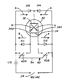
FIG. 2 ~s a circu~t ~iagram of an electronic
ballast circuit in accordance with the principles of
the pre~ent invention.
BEST MODE FOE~ CARRYING OUT THE IWVENTlOla
For 3 better understanding of the present
invention, together with other and further objects,
advantages and capabilities thereof, reerence is made
to the followin~ disclo~ure a~d appended claims in
conjunction with the accompanying drawings.
The present invention relates to an electronic
ballast circuit and in particular an improved
capacitive ballast for a discharge lamp such as a DC
glow lamp. Reference has been made in FIG. 1 to a
prior art capacitive ballast in which th~ discharge
current flows to essentially the same point on the
cathode during each half-cycle of the AC signal. The
pr~sent invention represents an improvement and in the
preferred embodiment, the improvement is disclosed in
FIG. 2 herein. The improved electronic ballast
circuit of the present invention is characterized by
improved cathode operation and overall lamp
operation. In this connection, rather than having the
single point dischar~e of the prior art circuit of
FIG. 1, there is provided in accordanc~ with the
present invention, in the preferred embodiment of FI~.
2, a double hot spot operation regime for the lamp
cathode, which has the advantage of better cathode
maintenance.
;~,~' ., ., ; .', . ,, . , . , .. . . ' '; ' ' , . . . , ' ! . . ' .'
;z~c)
D-88-1-235 -7- PATENT
Referring now to the specific circuit ~ FIG. 2,
it i~ compr~ed of a b~llast capacitor C10 and a
rectifi2r bridge that i~ essentially split into two
halves, thus allowing the ~ charge current to flow to
opposite ends of the filament (cathode) during
alternating h~lf-cycles.
In FI~. 2 the rectifier bridge is comprised Of
diodes Dll and D13 on one side and diodes D12 and Dl~
on the other ~ide. The cathode of diode Dll snd the
anode of D13 are coupled in common and to the
capacitor C10. The capacitor C10 also connect~ to one
of the input terminals 24. The anode of diode Dll
connects to one side of the cathode 34. The cathode
of diode D13 and the cathode of Dl~ are connected in
common to the anode 32 of the DC glow discharge lamp
30.
on the other side of the rectifier bridge, the
cathode of diode D12 and the anode of diode D14
connect in common and directly to one of the input
~erminals 24. The anode of diode D12 connects to the
opposite end of the cathode 34, that is opposite to
the connection of the diode Dll to the eathode 34.
The cathode of the diode D14 connects to the anode 32
of lamp 30.
As indicated previously, the improved electronic
~allast circuit of the present invention is
characterized by a ~plit rectifier bridge that enables
discharg~ current to flow to opposite ends of the
cathode during alternating half cycles. During
one-half of the cycle, the diode~ 12 and D13 are
conductive and the arrows A illustrate the discharge
path to end 34A of the cathode 34. During the other
8 0
D-88-1-235 -8- PATENT
half-cycle of the AC ~ignal, only the diodes Dll znd
D14 are con~uc~ive. The arrows B illustrate this
di~charge path from the an~de 32 to the opposite end
34B of the cathode 34.
With the particular bridge configuration of FIG.
2, it is noted that a ~omewhat different starter
circuit arrangement is employed. This includes, for
e~ample, two glow bottles or ~imilar starting aid.
These are illustrated in FIG. 2 by the switches 40A
and 40B. The ~witch 40A is across diode Dll and the
switch 40B is across diode D12. The use of two
switchPs rathsr than one presents no particular
problem in terms of lamp operationO
The application of an input AC voltage at
terminals 24 will cau~e a elosure of the ~witch action
devices 40A and 40B. The closure of ~his device will
short out the two diodes Dll and D12 and providsi an
estremely low resistance path through the lamp cathode
34. The AC current flowing through the cathode at
~hi~ time will cause the cathode to heat up
(preheat). A short time later (several seconds
depending on thsi switch action) the switching device
40 will open-circuit and the lamp will start with
current flo~ing throuqh the lamp and alternately
diodes D13, D12 and D14, Dll. At start up (preheat)
the capacitor C10 acts as a voltage divider element ;n
conjunction with the cathode 34 to supply preheat
current. During lamp operation the capacitor C10
behaves as a ballasting impedance with a magnitude of
l/j~C. A very large percentage of the l;ne voltage
2~
D-88-1-235 -9- PATENT
i~ ~ropped across the c~pacitor C10 during lamp
operation but, ~ue to the highsr Q factor inherent in
capacitor~, the power loss i~ much smaller than would
be the ca~e ~or an inductor in a similar situation.
Thu~, in accordance with the present invention,
there is proposed an improved capaciti~e ballasting
circuit employing a diode bridge, but one that is
reconfigured so as to provide discharge current
flowing to opposite ends of the filament during
alternatiny hal-cycles. Again, this is illustrated
by the arrows A and B in FIG. 2 showing alternating
discharge to opposite e~ds of the cathode filament.
This operation provides the desira~le effect of
forming two cathode spots during normal lamp
operation. By forcing the cathode to work in a double
hot ~pot mode during lamp operati~n, there is an
improvement in the maintenance o~ the cathode by
preventing continuous barium evaporation from any one
point on the cathode during lamp operation. The
double hot spots furthermore make for a more even
heatinq of the cathode by the discharge and thus
provide improved lamp maintenan~e and performance.
Whil~ there has been shown and described what is
at present considered the preferred embodiment of the
invention, it will be obvious to those skilled in the
art that various changes and modifications may be made
therein without departing f rom the invention as
def ined by the appended claims .
What is claimed is: