Note : Les descriptions sont présentées dans la langue officielle dans laquelle elles ont été soumises.
CA 02008946 1998-11-18
VAPOR-PHASE EPI'rA~TAT. GROWTH METHOD
FIELD OF THE lNV~ 'ION
This invention relates to a vapor-phase epitaxial
growth method (this method being hereinafter sometimes referred
to as "vapor-phase growth method"), in which a Groups III-V
compound semiconductor containing arsenic is epitaxially grown
in the vapor phase using a volatile compound of the Group III
(according to Mendelejeff's periodic table, hereinafter the
same) element and a volatile compound of the Group V element
containing arsenic, wherein arsenic trihydride (hereinafter
referred to as arsine) is used as an arsenic source. It also
relates to a field effect transistor (hereinafter abbreviated
as FET ) comprising a semiconductor substrate having thereon a
GaAs or Al~Gal~As (wherein 0 < x < 1) epitaxial crystal grown
by metalorganic vapor-phase growth as a buffer layer.
BACKGROUND OF THE INVENTION
Groups III-V compound semiconductors, e.g., GaAs,
AQ~GalxAs, GaAs~Pl~, In~Gal~As, and In~Gal~AsyPly, are extremely
useful as materials for Gunn diodes, ultra-high speed semi-
conductor devices, light-emitting devices, etc., and the demand
therefor has recently been considerably increasing. Compound
semiconductor epitaxial crystals for these devices are produced
by vapor-phase growth, molecular beam epitaxial growth, and
liquid-phase growth. In particular, the vapor-phase growth
~0~8g~6
method is attracting attention as an industrial method
applicable to mass production.
Known techniques of vapor-phase growth of Groups III-
Y compound semiconductors include (1) a metalorganic chemical
vapor deposition (hereinafter referred to as MOCVD) method in
which an alkyl compound of the Group III element and a hydride
or alkyl compound of the Group V element are heat decomposed,
(2) a hydride method using a chloride of the Group III element
and a hydride of the Group V element, and (3) a chloride method
using a chloride of the Group III element and a chloride of the
Group V element. In the production of compound semiconductors
containing arsenic by the MOCVD method and hydride method,
arsine is widely used as a source of arsenic. By combining
arsine with an alkyl compound of the Group III element in the
MOCVD method or with a chloride of the Group III element in the
hydride method, it is possible to grow a crystal exhibiting
satisfactory light emission characteristics and, hence,
industrial production of light-emitting devices, such as
semiconductor lasers and light-emitting diodes has already been
put into practice.
In particular, GaAs and A~sGalxAs (wherein 0 < x c 1)
compound semiconductors are of extreme use as materials of
ultra-high speed FET devices, and the demand therefor has
recently been increasing in the field of various amplifiers and
high-speed integrated circuits. FET devices for these
20(~9~
applications are generally produced by processing a GaAs or
A~Gal~As crystal layer formed on a semi-insulating single
crystal substrate through epitaxial growth so as to have
prescribed carrier concentration, thickness and composition.
The epitaxial crystal to be used in the FET device i5 produced
by vapor-phase growth, molecular beam epitaxial growth or
liquid-phase growth. In particular, the MOCVD method using an
organic metal and arsine as raw materials has been attracting
attention as an industrially applicable mass-production method.
In-the production of an epitaxial crystal for, for instance, a
high electron mobility transistor (hereinafter abbreviated as
HEMT~ which has been recently noted as one of ultra-high speed
FET according to the MOCVD method, arsine, trimethylgallium,
trimethylaluminum, and a dopant gas are successively supplied
onto a heated substrate of a GaAs single crystal and heat
decomposed to form a non-doped GaAs layer (about 0.5 ~m thick),
a non-doped Al03GaO.7As layer (0.001 to 0.02 ~m thick), an N~
type A~0.3Ga0.7As layer (0.03 to 0.05 ~m thick), and an N~type
GaAs crystal (0.05 to 0.15 ~m thick) through epitaxial growth
in a successive manner to thereby obtain a crystal having a
prescribed structure. Epitaxial crystals applicable to the
other FET devices can be prepared in a similar manner. Since
the crystal thickness and composition are easily and precisely
controllable by adjusting flow rates of raw material gases,
-- 3 --
;~0(~8~34~
the MOCV~ method is expected as an advantageous technique of
crystal growth for FET.
However, the conventional vapor-phase growth method
using arsine as a Group V source has poor reproducibility in
the formation of epitaxial crystals for use particularly in
high-speed electronic devices requiring a high purity layer
with a low impurity concentration. For example, in an FET used
as an amplifier in the ultra-high frequency band, an N-type
GaAs crystal active layer having an electron concentration of
fro~ about 1 to 2 x 10l~/cm3 is formed on a semi-insulating
substrate, and a high purity buffer layer having a thickness of
from about 0.2 to 5 ~m is usually inserted between the
substrate and the active layer as described in Gallium Arsenide
And Related ComPounds (1976), Institute of Ph~sics Conference
Series, No. 33b, pp. 11-12. In order to prevent impurities in
the substrate from exerting adverse influences on the active
layer and to reduce a leakage current through the buffer layer,
the buffer layer must be comprised of a high resistance crystal
having a carrier concentration arising from residual impurities
of not more than about 2 x 10l4/cm3. Where the crystal for FET
is allowed to grow by the MOCVD method, however, despite the
crystal growth conditions so selected as to i ni i ze the
carrier concentration of the buffer layer, it has been
difficult to decrease it below 2 x 10l4 cm/3, which is
considered to constitute a cause of inferiority in FET
C~o~ 6
characteristics. This has placed a hindrance to industrial
utilization of crystals obtained by the MOCVD method in FE~r for
low noise amplifiers. Similarly, in the case of applying the
crystals to high-output FET for power, FET for integrated
circuits, etc., reduction in power efficiency and scatter of
threshold voltage which are considered attributed to the
shortage of buffer layer resistivity have been pointed out.
In order to solve these problems, it has been attempted to add
a dopant forming a deep level in the forbidden band of the
gro~ing buffer layer crystal to thereby reduce the residual
carrier concentration by impurity compensation as taught in
Journal of Crystal Growth, Vol. ~4, pp. 29-36 (1978). However,
satisfactory characteristics have not yet been attained due to
influences from the deep level formed by the compensating
dopant which is introduced into the buffer layer in a large
quantity and due to transfer of the compensating dopant to an
active layer which is subsequently formed on the buffer layer.
From the viewpoint of vapor-phase growth, a silicon
impurity in the organic metal raw material is known as one of
causes of the high residual carrier concentration in non-doped
crystals formed by the MOCVD method and, hence, reduction of
a silicon impurity in the raw material has been studied for
improving crystal characteristics as described in Journal of
Crystal Growth, Vol. 55, pp. 255-262 (1981). Nevertheless,
even those crystals prepared from an organic metal whose
-- 5 --
X~ 9~6
impurity chiefly comprising silicon has been considerably
reduced still suffer from scattering of crystal purity, proving
unsuitable for stable use as crystals for FET.
In the light of the above-described circumstances, it
has been demanded to produce a highly resistant crystal having
a low residual carrier concentration without using a
compensating dopant and to develop an FET using such a crystal
as a buffer layer.
The inventors had previously conducted extensive
studies to analyze causes why the epitaxial crystals prepared
by vapor-phase growth using arsine do not have stable purity
and are therefore unapplicable to devices requiring a high
purity layer. As a result, it had been found that the donor
impurity concentration in the epitaxial crystal is subject to
great variation with lot-to-lot variation of the arsine source
used as reported in Ths 46th Ohyo Butsuri Gakkai Yokoshu, 2a-
E-3 (1985). According to the inventors' studies, when various
crystal layers prepared using various arsine lots were applied
to FET as a buffer layer on trial, crystals obtained from the
most arsine lots turned out to be unsuitable for practical use.
This means that, in using commercially available arsine, a
deliberate choice should be made from various arsine lots
before one can prepare a crystal having desired characteristics
suited for use in FET with good reproducibility. Moreover,
even if any chose may be determined, since arsine lots suitable
for practical use are very few in number, it i8 difficult to
produce a desired crystal on an industrial scale. Therefore,
fxom the standpoint of industrialization of devices requiring
high purity crystals, such as high-speed electronic devices
including FET, it has been keenly demanded to stably supply
arsine of improved p-~rity and to develop a vapor-phase crystal
growth method by the MOCVD method or hydride method using such
high purity arsine.
Considering that the amount of impurities present in
arsine is extremely small, stable supply of high purity arsine
cannot be achieved unless one knows what and how much the
impurities are with no analytical means available, what kinds
of impurities are present, to what degree the impurities should
be reducedr and how to purify the arsine source. However, it
has been virtually impossible to solve these problems.
SUMMARY OF THE INVhN ~lON
An object of this invention is to provide a vapor
epitaxial growth method for industrially producing an epitaxial
crystal of a Groups III-V compound semiconductor cont~;ning
arsenic which has sufficient electron concentration and
mobility for application to a device requiring a high purity
crystal layer including a high-speed electronic device by using
arsine having a sufficient purity as an arsenic source.
Another object of this invention is to provide a GaAs
or A~xGalxAs (wherein 0 < x 1) epitaxial crystal suitable as a
2~ 89~6
buffer layer of a crystal for an FET, said epitaxial crystal
being prepared by an MOCVD method and having incorporated
thereinto no compensating impurity.
These and other objects and advantages of t~e present
invention would be apparent through the description hereinafter
given.
The present invention relates to a vapor epitaxial
growth method for producing a Groups III-V compound
semiconductor cont~ining arsenic by vapor-phase growth using
arsenic trihydride as an arsenic source, wherein said arsenic
trihydride has a volatile impurity concentration of not. more
than 1.5 molppb on a germanium tetrahydride conversion.
The present invention further relates to an epitaxial
crystal for an FET, which has a high resistance GaAs or
A~Gal~As (wherein 0 x < 1) epitaxial crystal as a buffer layer,
said GaAs or A~xGalxAs epitaxial crystal being prepared by an
MOCVD method and having a carrier concentration of not more
than 2 x 10l4/cm3.
BRIEF DESCRIPTION OF THE DRAWINGS
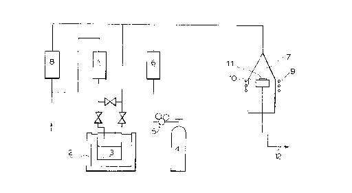
Figure 1 illustrates a schematic view of an apparatus
for vapor-phase growth which can be used in carrying out the
method of the present invention.
Figure 2 depicts the relationship between germanium
tetrahydride (GeH4, hereinafter referred to as germane) in
arsine gas and electron concentration in crystals.
20~89~6
Figure 3 depicts the relationship between re~idual
electron concentration in crystals obtained by vapor-phase
growth and As/Ga ratio while growth.
Figure 4 depicts the rslationship between carrier
concentration in crystals obtained in Examples and Comparative
Examples and As/Ga ratio.
Figure 5 depicts a carrier concentration profile in the
depth direction of crystals obtained in Examples and
Comparative Exa~ples.
Figures 6 through 9 each shows static characteristics
at room temperature of a recess gate type FET having a gate
length of 1 ~m obtained in Examples and Comparative Examples
(abscissa: drain voltage; ordinate: drain current).
Figures 10 and 11 each shows static characteristics of
an FET having a gate length of 1 ~m and using a selectively
doped epitaxial crystal obtained in Examples and Comparative
Examples (abscissa: drain voltage; ordinate: drain current).
Figure 12 shows an electron concentration profile in
the depth direction of the selectively doped epitaxial crystal
obtained in Comparative Example 3.
DETAILED DESCRIPTION OF THE INVENTION
The present invention will be illustrated with
reference to an MOCVD method as an instance, but the present
invention is not limited thereto.
Raw materials of the Group III which can be used in the
present invention include a trialkylgallium, e.g.,
trimethylgallium and triethylgallium; a tri(Cl-C4)alkyl-
aluminium, e.g., trimethylaluminum, triethylaluminum, and
tributylaluminum; and a trialkylindium, e.g., trimethylindium
and triethylindium, either individually or as a mixture
thereof. Commercially available Group III materials have high
purity causing no problem of purity of the resulting crystals
and can hence be employed in the present invention.
The Group V raw material which can be used in the
present invention is arsine cont~ining a volatile impurity in
a concentration of not more than 1.5 molppb, preferably not
more than 0.2 molppb, on a germane conversion. If desired,
arsine may be mixed with phosphine, antimony hydride (stibine),
etc. This being the case, the gas to be mixed also should have
a high purity.
Fig. 1 illustrates an example of an apparatus for
vapor-phase growth of GaAs according to an MOCVD method.
Embodiments of the present invention are now explained by
referring to Fig. 1.
Carrier gas under flow control by mass flow controller
1 is forwarded to bubbler 3 under temperature control by
thermostat 2, where the carrier gas is bubbled through a
trialkylgallium in the bubbler 3 and then carried to reactor 7
together with trialkylgallium vapors. At this time, the amount
-- 10 --
2~g~
of the trialkylgallium to be introduced is controlled to fall
within the range usually of from 10-3 to 10-5 mol/min by
adjusting the vapox pressure determined by the liquid
temperature and ~he flow ra~e of the carrier gas to be bubbled.
On the other hand, arsine is usually charged in
aluminum- or steel-made high pressure container 4. After
pressure adjustment by means of reducing valve 5, arsine is
introduced into the reactor 7 through mass flow controller 6
for flow rate ad~ustment. The amount of arsine to be
introduced is generally from 5 to 200 times that of the gallium
raw material. The arsine and trialkylgallium vapors are
generally forwarded to the reactor 7 together with a carrier
gas whose flow rate has been controlled by mass flow controller
8.
In the reactor 7 is placed graphite mount (susceptor)
10 which is subject to high-frequency heating by means of
external coil 9 set around the reactor 7. On heating, the
mixed gas of the raw material gases and the carrier gas is heat
decomposed in the vicinity of substrate 11 mounted on the
susceptor 10 to allow a GaAs epitaxial cr~stal to grow on the
substrate 11. The exhaust gas after the reaction is discharged
from exhaust port 12.
While the above example illustrates growth of GaAs,
epitaxial crystals of a broad range of Groups III-V compound
semiconductors containing arsenic can be obtained by supplying
89~6
a trialkylaluminium, a trialkylindium, etc. in place of the
trialkylgallium by the use of the same gas feeding mechanism as
used above or by supplying phosphine, stibine, etc. in place of
arsine by the use of the same gas feeding mechanism as used
above.
Metnods for analyzing impurities in crystals and in
arsine gas from which the former arises are described below in
detail.
GaAs was allowed to grow by epitaxy using the apparatus
o~ Fig. 1 and commercially available arsine as an arsenic
source. In using trimethylgallium as a gallium source,
electrical characteristics of the resulting crystal layer vary
depending on the arsine/trimethylgallium feed ratio. Namely,
as far as the As/Ga ratio (arsine to tri~ethylgallium ratio) is
small, the crystal layer is of P-type. According as the As/Ga
ratio increases, the layer becomes an N-type, and the electron
concentration monotonously increases with a further increase
of As/Ga ratio. The As/Ga ratio at which the crystal changes
from P-type to N-type varies depending on growth conditions and
the raw material lot. With the growth conditions being
appropriately fixed, such an As/Ga ratio substantially depends
on the arsine lot used and is subject to variation between the
range of from about 15 to 40 as hereinafter described. N-type
crystals are usually obtained at an As/Ga ratio of 50. The
acceptor impurity in these N-type crystals is known to be
20(~89~Ç~
carbon arising from methyl groups of trimethylgallium as
described in Journal of CrYstal Growth, Vol. 68, pp. 148-156
(1984), and it is considered that the crystal becomes P-type
predominantly because of increased incorporation of the carbon
atoms into the crystal at a low As/Ga ratio. As the As/Ga
ratio increases, the carbon acceptor decreases, and the crystal
purity comes under government of a donor impurity, but the
origin and composition of the donor impurity have been unclear.
Hence, the following analyses were conducted in order
to find the impurity in N-type crystals rich in donor impurity.
An N-type crystal (d~signated Sample A) was prep~red using a
certain arsine lot at a growth temperature of 650~C and at an
As/Ga ratio of 50. The electron concentration attributed to
the residual donor impurity in Sample A was found to be
3.3 x 10l6/cm3 by a capacitance-voltage (C-V~ method. Then,
impurity in Sample A was analyzed by secondary ion mass
spectrometry. As a result, g~rm~nium, silicon, and sulfur out
of the Groups IV and VI elements which are believed to act as
donor impurities in GaAs were detected at concentrations of
2.3 x 10l6/cm3, 0.6 x 10l6/cm3, and 0.3 x 10l6/cm3, respectively.
From the fact that the sum of these concentrations is almost
consistent with the residual electron concentration above
obtained, it is assumed that the residual donor impurity in
Sample A chiefly arises from ge -nium~ silicon, and sulfur.
39~6
: Further, samples differing in purity prepared using
several different arsine lots were analy~ed to find donor
impurity by far infrared photo-conductivity spectrometry. A~
a result, even those samples of higher purity showed donor
peaks assigned to germanium, silicon, and sulfur having a total
intensity corresponding to the residual elec$ron concentration.
It was thus proved that the donor impurity arising from arsine
always comprises g~rr~nium, silicon, and sulfur.
From these analytical results, it can be seen that a
GaAs crystal grown using commercially available arsine contains
gerr~n;um, silicon, and sulfur as a main donor impurity at a
total concentration being almost consistent with the residual
electron concentration in the crystal under certain fixed
growth conditions and that the impurity arises from the
impurity of arsine. However, impurity analyses of arsine by
gas chromatography and infrared absorption spectrophotometry
which have been conventionally employed for analyzing arsine
failed to detect impurities corresponding to ge ~nium,
silicon, and sulfur probably because the amounts of these
impurities are extremely low below the detection limits of
these analytical methods. Since no definition for such traces
of impurity has hitherto been proposed, a new definition of
impurity in arsine which exerts influences on epitaxial
crystals should be established before closer studies can be
conducted.
- 14 -
, .
~8~9~6
Utili~ing the facts that the residual electron
concentration in a GaAs epitaxial cr~stal i8 sensitive to the
impurity concentration under proper growth conditions and that
electron concentrations can be measured with an extremely high
sensitivity, the inventors have established a method ~or
evaluating purity of arsine as follows. That is, ~aAs growth
conditions under which the impurity in arsine makes a large
contribution to a residual electron concentration while other
impurities make small contributions thereto were selected, and
the electron concentration of a crystal grown under such
conditions was measured to evaluate arsine purity.
Then, GaAs was allowed to undergo epitaxial growth
using a number of commercially available arsine lots at
present, and the residual electron concentration of each of the
resulting epitaxial crystals was obtained by the C-V method.
A concentration o~ the impurity in arsine was then to be
estimated. Although it is assumed that the germanium, silicon
and sulfur impurities in the crystal may probably have had a
molecular form of hydride while in arsine, the actual state is
still unknown. Hence, the inventors made it a rule to express
the amount of the impurity in arsine as follows. Germane-doped
GaAs crystals were prepared under the same growth conditions as
specified above with a varied germane amount, and the amount of
germane necessary to obtain the same electron concentration as
the residual electron concentration in the crystal prepared
- 15 -
~0~ 6
using arsine under analysis was divided by the amounk of arsine
used. The quotient is taken as an indication of arsine purity
(explained more speci~ically in Reference Example hereinafter
described). An arsine lot from which a crystal having a
relatively low electron concentration was obtained was chosen
as a standard. GaAs was allowed to grow by epitaxy using the
standard arsine while introducing a germane standard gas
(diluted with hydrogen) having a known concentration as a
dopant gas at a varied feed rate. The electron concentration
of each of the resulting crystals was measured by the C-V
method to give a substantially linear proportional relationship
between the germane concentration in arsine and a difference
between the residual electron concentration of the resulting
crystal and that of the crystal obtained by using the standard
arsine as shown in Fig. 2. By using this relationship as a
calibration curve, an impurity concentration in a commercially
available arsine lot under analysis on a germane conversion can
be obtained from the residual electron concentration in the
crystal prepared by using that arsine.
Further, characteris~ics of crystals prepared by using
an arsine lot whose impurity concentration is known by the
above-described method were closely e~ ined to reveal the
following facts. ~s explained above with respect to the
analyses, a crystal prepared from a combination with
trimethylgallium changes its electrical characteristics from P-
_ 16 -
201~9~6
type to N-type with a change of an As/Ga ratio (a quotient
obtained by dividing an arsine feed by a trimethylgallium feed,
hereinafter the same) during growth. With the change from P-
type to N-t~pe, the carrier concentration drastically decreases
due to compensation between donor impurities and a ceptor
impurities. Accordingly, the change can be made use of in the
production of a buffer layer of a crystal for a high-frequency
FET or an active layer of a Gunn diode which requires be to a
high-resistant layer having a carrier concentration of, for
instance, not more than l to 2 x l014/cm3. However, in using
arsine having a high impurity concentration, for example, of
9.2 molppb on a germane conversion, the change from P-type to
N-type of higher electron concentration suddenly took place in
the vicinity of As/Ga = l0 as shown in Fig. 3-(a). It was
therefore difficult to obtain crystals having a carrier
concentration of not more than 2 x l0l4/cm3 with good
reproducibility. On the other hand, where arsine of low
impurity concentration was used, as shown in Fig. 3-(b), the
As/Ga ratio causing the P-type to N-type change became higher
and, also, the carrier concentration at around that As/Ga ratio
became lower, thus making it easy to obtain a crystal of
desired purity. This tendency becomes conspicuous according as
the impurity concentration of arsine decreases. After
ex.periments in more detail, it was proved that a high purity
crystal having a residual electron concentration of not more
- 17 -
Z0~89~i
than 2 x 10~4~cm3 can be obtained with satisfactory
reproducibility by properly controlling the As/Ga ratio
according to the purity of arsine used as long as the arsine
has an impurity concentration of not more than 1.5 molppb. It
also turned out that where arsine used has an impurity
concentration of not more than 0.2 molppb, a high purity
crystal containing a reduced remaining impurity can be obtained
with satisfactory reproducibility by selecting the As/Ga ratio
from a broad range of from 20 to 80. From these results, it
has,now been ascertained that an arsine source to be used in
obtaining high purity crystals applicable to high-speed
electronic devices, such as FET and Gunn diodes must have an
impurity concentration of not more than 1.5 molppb, and
preferably not more than 0.2 molppb, on a germane conversion.
A method for preparing the above-described high purity
arsine which can be used in vapor-phase growth according to the
present invention is described below.
According to the inventors' studies, fractional
distillation of arsine gives an initial boiling point fraction
having a high impurity concentration while giving an end point
fraction and a still residue each having a low impurity
concentration. Therefore, arsine having a markedly reduced
impurity can be obtained by recovering a high-boiling fraction
or a still residue in general fractional distillation or batch
distill~tion. High purity arsine can also be obtained by
- 18 -
,
:-
.
9~6
precise fractional distillation by means of a rectificationtower using a packed column. Conditions for distillation are
appropriately selected without any particularly limitation.
Taking vapor pxessure of arsine into consideration, it is
usually preferable to conduct distillation under a pressure of
from atmospheric pressure to 10 kg/cm2G.
Tllus, high purity arsine of desired purity as having a
donor impurity concentration of not more than 1.5 molppb, and
preferably not more than 0.2 molppb, on a germane conversion
can~be supplied in a stable manner irrespective of the purity
of commercially available arsine lots, thus making it possible
to stably obtain a high purity crystal applicable to an FET,
a Gunn diode, etc. by vapor-phase growth.
While the foregoing explanation relates to growth of
high purity GaAs by the MOCVD method, the same effects as
described above can be produced when vapor-phase growth is
carried out by a hydride method also using arsine as a raw
material.
As described abovel in vapor-phase growth of an
epitaxial crystal of a Groups III-V compound semiconductor
containing arsenic using arsine as an arsenic source, use of
high purity arsine containing a volatile impurity containing
germanium, silicon, and sulfur at a concentration of not more
than 1.5 molppb on a germane conversion as an arsenic source
makes it feasible to stably supply a high purity epitaxial
-- 19 --
20(~89~6
crystal which can be applied to high-speed electronic device~
including an FET. Thus, combined with the above-described
method for supplying high purity arsine according to the
present invention, the present invention is of great industrial
significance.
The present invention is now illustrated in greater
detail with reference to Reference Example, Examples, and
Comparative Examples, but it should be understood that the
present invention is not to be construed as being limited
thereto.
REFERENCE EXAMPLE
An experiment was conducted as follows by the use of an
apparatus for vapor-phase growth as shown in Fig. 1.
GaAs was allowed to grow on a substrate comprising a
semi-insulating GaAs single crystal at a substrate temperature
of 650~C for 120 minutes while feeding 6.7 x 10⁻⁵ mol/min of
trimethylgallium, 3.35 x 10⁻³ mol/min of commercially available
arsine, and 15 l/min of a carrier hydrogen gas to obtain a 6 ~m
thick epitaxial GaAs crystal. Electrical characteristics of
the resulting crystal were determined by the C-V method (at
room temperature) and, as a result, the residual electron
concentration was found to be 1.8 x 10¹⁵/cm3. Then, to the
arsine used above was added a varied amount of germane standard
gas (diluted with hydrogen) having a known concentration, and
vapor-phase growth was carried out under the same conditions as
- 20 -
20(~89~
described above but using each of the mixed gases having
various germane concentrations shown in Table 1 below. The
residual electron concentration of each of the resulting
crystals was measured. A difference between the measured
residual electron concentration and the residual electron
concentration of the crystal obtained by using only arsine
(i.e., 1.8 x 10l5/cm3) is shown in Table 1. A plot of
difference in residual electron concentration vs. germane
concentration in the logarithmic expression gave a straight
line as shown in Fig. 2 and proved usable as a calibration
curve. In Examples and Comparative Examples hereinafter
described, impurity concentrations of arsine on a germane
conversion were obtained by using the calibration curve thus
prepared.
TABLE 1
Difference in Residual
GeH/,/AsH3Electron Concentration Remarks
(molppb) (cm~')
13 3.7 x 10¹⁵ 0.1 ppm GeH4
was used.
52 1.7 x 10l6 "
130 3.7 x 10l6 "
520 1. 6 X lol7 1 . O ppm GeH4
was used.
1300 3.3 x 10¹⁷ ..
20~R9~6
EXAMPLE 1
(1) Purification of Arsine.
(a) A GaAs epitaxial crystal was allowed to grow on a
semi-insulating GaAs single crystal substrate at a suhstrate
temperature of 650~C for 120 minutes by means of the apparatus
shown in Fig. 1 by feeding 6.7 x 10⁻⁵ mol~min of
trimethylgallium, 3.35 x 10⁻³ mol/min of commercially available
arsine and 15 Q/min of a carrier hydrogen gas to obtain a 6 ~m
thick epitaxial GaAs crystalO Electrical characteristics of
the resulting crystal were ~x~ ;ned by Hall measurement using
the Van der Pauw configuration and C-V measurement. As a
result, the crystal was found to be of an N-type and to have an
electron concentration of 2.4 x 10l5/cm3 and an electron
mobility of 7,400 cm2/V sec at room temperature. From the
electron concentration thus measured in view of the calibration
curve of Fig. 2, the impurity concentration in the arsine was
found to be 8.0 molppb on a germane conversion.
(b) About 1 kg of the above arsine was subjected to
batch distillation under a pressure of 0.5 kg/cm2G to obtain a
still residue weighing 232 g.
Epitaxial growth of GaAs was carried out in the same
manner as in (a) above but using the thus purified arsine as an
arsenic source, and the electron concentration of the resulting
crystal was measured. As a result, the purified arsine was
~ 22 -
ZC~C~8~6
found to have an impurity concentration of 0.14 molppb on a
germane conversion.
(2) Crystal Growth:
Crystal growth on a semi-insulating GaAs single crystal
substrate was carried out at a substrate temperature of 650~C
for 120 minutes by means of the apparatus of Yig. 1 by feeding
6.7 x 10⁻⁵ mol/min of trimethylgallium, 6.7 x 10⁻⁴ to
5.4 x 10⁻³ mol/min (corresponding to an As/Ga ratio of from 10
to 80) of the purified arsine as obtained in (l)-(b~ above
(impurity concentration: 0.14 molppb on a germane conversion),
and 15 ~/min of a carrier hydrogen gas to obtain a 6 ~m thick
epitaxial crystal. Evaluation of the electrical
characteristics of each of the resulting crystals revealed a
relationship between the residual carrier concentration of each
crystal and the As/Ga ratio during growth as shown in Fig. 4-
(a~. The conduction type of the resulting crystals changed at
an As/Ga ratio of about 50. Within an As/Ga ratio of from 20
to 80, the carrier concentration was 1 x 10l4/cm3 or less,
indicating that the crystals had a high purity suited for use
in high-speed semiconductor devices.
~3) Crystal Growth for FET and Evaluation:
(a) An apparatus shown in Fig. 1 which additionally
comprised a means for supplying monosilane (silicon tetra-
hydride) diluted with hydrogen to 20 molppm (the mechanism was
the same as in the arsine feeder) was employed. Crystal growth
- 23 -
.
Z ~ ~ 9~ 6
on a semi~insulating GaAs single crystal substrate was carried
out at a substrate temperature of 650~C by feeding 6.7 x 10⁻⁵
mol/min of trimethylgallium, from 1.4 to 3.4 x 10⁻⁴ moltmin of
the purified arsine as obtained in (l)-(b) (corresponding to an
As/Ga of from 20 to 50), and 15 ~/min of a carrier hydrogen gas
to form a non-doped GaAs layer having a thickness of 3 ~m.
Then, 8.9 x 10⁻⁸ mol/min of monosilane was subsequently fed for
doping to grow an N-type layer to a thickness of 0.5 ~m. As a
result of Hall measurement of each of the resulting samples at
room temperature, the electron mobility and the sheet carrier
concentration were 3,900 cm2/V sec and 5 x lol2/cm2
respectively, irrespective of the arsine feed rate.
(b) Each of the samples was subjected to etching to a
depth of about 0.6 ~m while leaving the electrode portion
thereof unetched to ~ ~ve the N-type doped layer. The
remaining non-doped GaAs layer was found to have a resistivity
of l x 103 ohm-cm or more, proving to have a satisfactory
resistivity.
(c) An electron concentration profile of each sample
was determined by the C-V method to obtain a satisfactory
profile as shown in Fig. 5-(a).
(d) A recess gate type FET having a gate length of l ~m
and a gate width of 250 ~m was prepared by using the above
obtained crystal. Dete inAtion of static characteristics of
the resulting FET gave satisfactory results as shown in Fig. 6
- 24 -
20~ 6
with drain voltage (Vds: 2 ~/div.) as abscissa and drain
current (Ids: 5 mA/div.) as ordinate. As a parameter (Vg8 ),
the gate voltage was varied by a 500 mV step.
(e) The gate electrode was removed from the FET, and a
groove of 0.6 ~m deep and 5 ~m width was made between the
source electrode and the drain electrode (about 10 ~m apart).
A drain-source leakage current was measured. The lPakage
current on application of 10 V was 2.5 x 10⁻⁹ A.
It can be seen from these results that a high purity
GaAs crystal suitable for use in an FET for high-frequency
amplification can be obtained when purified arsine having an
impurity concentration of 0.14 molppb on a germane conversion
is used as an arsenic source.
EXAMPLE 2
(1) Purification of Arsine:
(a) A commercially available arsine lot different from
that used in Example 1 was analyzed in the same manner as in
Example 1. As a result, it had an impurity concentration of
15.2 molppb on a germane conversion.
(b) About 1 kg of the above arsine was subjected to
batch distillation in the same manner as in Example l-(b).
Epitaxial growth of GaAs was carried out in the same manner as
in Example l-(a) but using the thus purified arsine to find
that the purified arsine had an impurity concentration of
1.4 molppb on a germane conversion.
- 25 -
X(~89~,
(2) Crystal Growth:
Crystal growth was carried out in the same manner as in
Example 1-(2), except for using the purified arsine (impurity
concentration: 1.4 molppb on a germane conversion). Evaluation
of electrical characteristics of the resulting crystal gave the
relationship of residual carrier concentration vs. As/Ga ratio
as shown in Fig. 4-(b). The conduction type of the resulting
crystal changed at an As/Ga ratio of about 20. Within an As/Ga
ratio of from 20 to 40, the crystal had a carrier concentration
was not more than 2 x 10l4/cm3, proving to have a high purity
suitable for use in high-speed semiconductor device~.
(3) Crystal Growth for FET and Evaluation:
(a) An apparatus ~hown in Fig. 1 which additionally
comprised a means for supplying monosilane diluted with
hydrogen to 20 molppm (the mechanism was the same as in the
arsine feeder) was employed. Crystal growth on a semi-
insulating GaAs single crystal substrate was carried out at a
substrate temperature of 650~C by feeding 6.7 x 10⁻⁵ mol/min of
trimethylgallium, from 1.4 to 3.4 x 10⁻⁴ mol/min of the purified
arsine as obtained in (l)-(b) above (corresponding to an As/Ga
of from 20 to 50), and 15 ~/min of a carrier hydrogen gas to
form a non-doped GaAs layer having a thickness of 3 ~m. Then,
8.9 x 10 8 mol/min of monosilane was subsequently fed for doping
to grow an N-type layer to a thickness of 0.5 ~m. As a result
of Hall measurement of each of the resulting samples at room
- 26 -
2 ~ ~ ~ 9 ~Ç~
temperature, the electron mobility and the sheet carrier
concentration were 3,900 cm2/V sec and 5 x 1ol2/cm3
respectively, irrespective of the arsine feed rate.
(b) Each of the samples was subjected to etching to a
depth of about 0.6 ~m while leaving the electrode portion
thereof unetched to remove the N-type doped layer. The
r~qining non-doped GaAs layer of each of the samples prepared
at an As/Ga ratio of from 20 to 30 was found to have a
resistivity of 1 x 10³ ohm-cm or more, proving to have a
satisfactory resistivity. The resistivity of those samples
prepared at a higher As/Ga ratio was from 1 to 100 ohm-cm.
(c) An electron concentration profile of each sample
prepared at an As/Ga ratio of from 20 to 30 was determined by
the C-V method to obtain a satisfactory profile as shown in
Fig. 5-(b)-
(d) A recess gate type FET having a gate length of 1 ~mand a gate width of 250 ~m was prepared by using the crystal
obtained at an As/Ga ratio of from 20 to 30. Static
characteristics of the resulting FET were determined in the
same manner as in Example l-td) to obtain satisfactory results
as shown in Fig. 7.
(e) The gate electrode was removed from the FET, and a
groove of 0.6 ~m deep and 5 ~m width was made between the
source electrode and the drain electrode (about 10 ~m apart).
- 27 -
;
xo~9~
A drain-source leakage current was measured. The leakage
current on application of 10 V was 1 to 3 x 10⁻⁸ A.
It can be seen from these results that a high purity
GaAs crystal suitable for use in an FET for high--frequency
amplification can be obtained when purified arsine having an
impurity concentration of 1.4 molppb on a germane conversion is
used as an arsenic source.
COMPARATIVE EXAMPLE 1
(1) Crystal Growth:
- Crystal growth was carried out in the same manner as in
Example 1-(2), except for using the same commercially available
unpurified arsine as used in Example 1-(1) (impurity
concentration: 8.0 molppb on a germane conversion). Evaluation
of electrical characteristics of the resulting crystal gave the
relationship of residual carrier concentration vs. As/Ga ratio
as shown in Fig. 4-(c). The conduction type of the crystal
changed from P-type to N-type at an As/Ga ratio of around 10,
and the i ni carrier concentration was 1 x 10l5/cm3.
(2) Crystal Growth for FET and Evaluation:
(a) Crystal growth was carried out in the same manner
as in Example 1-(3), except for using the same commercially
available unpurified arsine (impurity concentration: 8.0 molppb
on a germane conversion). As a result of Hall measurement at
room temperature, the resulting crystal was found to have an
- 28 -
20~39~
electron mobility of 3,900 cm2/v- sec and a sheet carrier
concentration of 5 x 10l2/cm3 irrespective of the arsine feed.
(b) The sample was subjected to etching to a depth of
about 0.6 ~m while leaving the electrode portion thereof
unetched to remove the N-type doped layer. The r~m~i n i ng non-
doped GaAs layer was found to have a resistivity of 1 to 100
ohm cm.
(c) An electron concentration profile of each sample
prepared at an As/Ga ratio of from 20 to 30 was determined by
the C-V method, and the results are shown in Fig. 5-~c). It
can be seen that a part of the samples showed a satisfactory
profile, whereas other samples revealed a shoulder of about
1 x 10¹⁵/cm3 in the buffer layer thereof.
(d) A recess gate type FET having a gate length of 1 ~m
and a gate width of 250 ~m was prepared by ~sing each of the
crystals obtained at an As/Ga ratio of from 20 to 30. Static
characteristics of the resulting FET were determined in the
same manner as in Example 1-(d), and the results are shown in
Fig. 8. It can be seen that the FET exhibited slightly
deteriorated pinch-off characteristics, which are believed to
be ascribed to current leakage in the buffer layer.
te) The gate electrode was removed from the FET, and a
groove of 0.6 ~m deep and 5 ~m width was made between the
source electrode and the drain electrode (about 10 ~m apart).
- 29 -
X(~9~6
A drain-source leakage current was measured. The leakage
current on application of lO V was 1 x 10⁻⁴ to 3 x 10⁻⁵ A.
These results show difficulty of obtaining a high
purity crystal applicable to an FET, etc. with the arsine as
employed.
COMPARATIVE EXAMPLE 2
(1) Crystal ~rowth:
Crystal growth was carried out in the same manner as in
Example 1-(2), except for using the same commercially available
unpurified arsine as used in Example 2-(1) (impurity
concentration: 15.2 molppb on a germane conversion).
Evaluation of electrical characteristics of the resulting
crystal gave the relationship of residual carrier concentration
vs. As/Ga ratio as shown in Fig. 4-(d). The conduction type of
the crystal changed from P-t~pe to N-type at an As /Ga ratio of
around 10, and the i ni carrier concentration was
2 x 10~5~cm3
(2) Crystal Growth for FET and Evaluation:
(a) Crystal growth was carried out in the same manner
as in Example 2, except for using the same commercially
available unpurified arsine as used in Example 2 (.impurity
concentration: 15.2 molppb on a germane conversion). As a
result of Hall measurement at room temperature, the resulting
crystal was found to have an electron mobility of
- 30 -
X0(~89~6
3,900 cm /V sec and a sheet carrier concentration of 5 x 10l2/cm3
irrespective of the arsine feed.
(b) The sample was subjected to etching to a depth of
about 0.6 ~m while leaving the electrode portion thereof
unetched to remove the N type doped layer. The r~i n ing non-
doped GaAs layer was found to have a resistivity of l to 100
~ ohm-cm.
- (c) An electron concentration profile of each sample
prepared at an AstGa ratio of from 20 to 30 was determined by
the C-V method, and the results are shown in Fig. 5-(d). It
can be seen that a part of the samples showed a satisfactory
profile, whereas other samples revealed a shoulder of about
1 to 2 x lOls/cm3,
(d) A recess gate type FET having a gate length of 1 ~m
and a gate width of 250 ~m was prepared by using each of the
crystals obtained at an As/Ga ratio of from 20 to 30. Static
characteristics of the resulting FET were dete ined in the
same manner as in Example l-(d), and the results are shown in
Fig. 9. It can be seen that the FET exhibited slightly
deteriorated pinch-off characteristics, which are believed to
be ascribed to current leakage in the buffer layer.
(e) The gate electrode was removed from the FET, and a
groove of 0.6 ~m deep and 5 ~m width was made between the
source electrode and the drain electrode ~about 10 ~m apart).
- 31 -
;
2e~ 39~6
A drain-source leakage current was measured. The leakage
current on application of 10 V was 1 x 10⁻³ to 6 x 10⁻⁵ A.
These results show difficulty of obtaining a high
purity crystal applicable to an FET, etc. with the arsine as
employed.
EXAMPLE 3
A commercially available arsine lot was analyzed in the
same manner as in Example 1-(1) to find that the impurity
concentration thereof was 6.7 molppb. This arsine was purified
under the same conditions as in Example 1-(1). The impurity
concentration of the thus purified arsine was found to be
0.16 molppb.
A crystal for an HEMT was prepared using the purified
arsine and evaluated as follows.
Crystal growth was carried out at a substrate
temperature of 650~C by feeding 2.7 x 10⁻⁵ mol/min of
trimethylgallium, 15 ~/min of a carrier hydrogen gas, and
arsine at a feed rate corresponding to an As/Ga ratio of 50 for
25 minutes to grow non-doped GaAs ~thickness: 5,000 A). Then,
6.8 x 10⁻⁶ mol/min of trimethylaluminum was additionally fed for
5 seconds to grow non-doped A~GaAs (thickness: 20 A ) . Sub-
sequently, 8.9 x 10⁻⁸ mol/min of monosilane was additionally
fed for 2 minutes to grow N-type AIGaAs (thickness: 500 A).
Finally, the trimethylaluminum feed was stopped, and N-type
- 32 -
~o~g~
GaAs was allowed to growth for 7.5 minutes (thickne~s:
1,500 ~).
The N-type GaAs layer (uppermost layer) of the
resulting crystal was removed by etching, and Hall measurement
was conducted. As a result, the sheet carrier concentration
and electron mobility at 77 K were found to be 1.0 to
1.1 x 10¹²/cm2 and 40,000 to 42,0Q0 cm2/V sec, respectively.
An FET having a gate length of 1 ~m was prepared in the
same manner as in Example l-(d), except for using the above
obtained crystal. Det~ ;n~tion of static characteristics of
the resulting FET gave satisfactory results as shown in Fig.
10 .
COMPARATIVE EXAMPLE 3
Crystal Growth was carried out in the same manner as in
Example 3, except for using the same commercially available
arsine having an impurity concentration of 6.7 molppb as used
in Example 3. As a result of Hall measurement, the crystal
had a sheet carrier concentration of 1.1 to 1.2 x 10~2/cm2 and
an electron mobility at 77 K of 33,000 to 37,000 cm2/V- sec.
Then, an FET having a gate length of 1 ~m was prepared
in the same manner as in Example l-(d), except for using the
above obtained crystal. Dete in~tion of static
characteristics of the resulting FET revealed deterioration of
pinch-off characteristics and reduction of mutual conductance
at a high gate bias.
- ' .
89~6
The carrier concentration profile of the crystal was
. obtained by the C-V method. As shown in Fig. 12, a shoulder of
- carrier concentration which is considered ascribable to
impurity of the buffer layer was observed.
While the invention has been described in detail and
with reference to specific embodiments thereof, it will be
apparent to one skilled in the art that various changes and
modifications can be made therein without departing from the
- spirit and scope thereof.
- 34 -