Note : Les descriptions sont présentées dans la langue officielle dans laquelle elles ont été soumises.
2~Z9~9
MAGNETIC REPRODUCING HEAD AMPLIFIER
FIELD OF THE INVENTION
The present invention relates to a magnetic
reproducing head amplifier for amplifying FM carriers,
more concretely FM carriers which carry wide-band
frequency signals such as HDTV(high definition television)
signals, reproduced from a magnetic tape by a magnetic
head in a VTR(video tape recorder).
BACKGROUND OF THE INVENTION
As a VTR for recording and reproducing image signals
of a standard television system, there is known an
apparatus which has a circuit configuration shown in Fig.
7 including a magnetic reproducing head amplifier 53
(hereinafter called first prior art).
In the first prior art, image signals reproduced from
3~ '
., ~
..
2~69
a magnetic tape(not shown) by a magnetic head 51 located
on a rotary drum are entered to a magnetic reproducing
head amplifier 53 through a rotary transformer 52 composed
of a rotor on the rotary drum and a stator on a fixed
drum, and are released therefrom through a reproducing
amplifier 54 and an equalizer 55 after being amplified by
the magnetic reproducing head amplifier 53.
An equivalent circuit o~tained by reducing the
circuit shown in Fig. 7 at the secondary side(stator side)
of the rotary transformer 52 is shown in Fig. 8, where a
stray capacitance at the rotor side is omitted. In the
figure, C1~ represents an input capacitance of the
magnetic reproducing amplifier 53; in the same manner, C~1
as well as C~z: stray capacitance to ground of signal
wiring; L~: a head inductance of the magnetic head 51;
R~: a head resistor of the magnetic head 51(corresponding
to a head loss); n: turn ratio; the secondary side to the
primary side(stator side to rotor side) of the rotary
transformer 52; L2: a coil inductance at the secondary
side of the rotary transformer 52; L~: a leakage
inductance of the rotary transformer 52.
In the above, since LT nZ-L~ << L2 are satisfied
within the range of n = 1 to 1.5(n: turn ratio), the
equivalent circuit shown in Fig. 8 is simplified into the
one shown in Fig. 9. Now C~ represents the reduced input
,
~` 3 Z012~69
capacitance of an amplifier including the input
capacitance C1~, stray capacitances to ground Col and C~2,
and other capacitances. The resonance peak frequency fO
of the above resonance circuit is normally set at the
vicinity of the upper limit of FM carrier transmission
band as shown in a curve ~A) in Fig. 10, for example, by
the use of an externally attached capacltor 56. However,
these days it is rear to especially install the capacitor
56, and in the case where the capacitor 56 is not used,
the sensitivity is heightened by increasing the coil
inductance L~.
Generally, in the magnetic reproducing head amplifier
53 of a standard television system, when there is a
resonance peak frequency fO within a transmission band for
FM carrier, it is difficult to simultaneously perform an
inverted compensation for resonance characteristic (to
restore a preferable characteristic of amplifier
frequency) and a head aperture compensation as its
original purpose, that is, an equalization compensation,
only by the use of the equalizer 55. Therefore, at first,
in order to dump a resonance characteristic, dividing
resistors 57 and 58 as well as a negative feedback
resistor 59 are installed as shown in Fig. 7, and by
properly setting the values of these resistors, without
decreasing the CN ratio for the FM carrier and with
~ 4
2012969
dispersions of the reproducing sensitivity or other
characteristics of the magnetic head 51 being controlled,
a gain frequency characteristic of the magnetic
reproducing head amplifier 53 is flattened as shown in a
curve (B) in Fig. 10, and then the equalization
compensation in high frequency range is performed by FM
equalization in the equalizer 55.
Moreover, in order to shift the upper limit of the
frequency transmission band for an FM carrier to the
higher frequence side, by adding a capacitor 60 for
widening band width, as shown with dotted lines in Fig. 7,
the gain-frequency characteristic (B) of the magnetic
reproducing head amplifier 53 is shifted to have a wider
band as shown in a curve (D) in Fig. 10, and such a
resonance characteristic as shown in a curve (C) is
obtained by the equallzation compensation at the equalizer
55.
on the other hand, in a VTR for recording and
reproducing wide-band image signals such as HDTV baseband
signals having a luminance signal band width of 20MHz, for
example, TCI(Time Compressed Integration) signals having a
baseband width 12MHz are divided into two channels in its
band width, and frequency modulation is performed on their
respective carriers. However, FM carrier spectrum for
each channel has a wide-band distribution characteristic
, . .. . . .
Z012969
ranging from a lower vicinity of 6MHz to a higher vicinity
of 30MHz even in the first side band, supposing, for
example, 18MHz is a central carrier frequency, and
therefore it is necessary for the magnetic reproducing
head amplifier to have a wide-band frequency
characterlstic to deal with the above band width.
one example of the configuration of a VTR for HDTV is
shown in Fig. 11. Referring to the example of the
configuration(hereinafter called the second prior art) in
Fig. 11, in reproduction, an FM carrier for HDTV
reproduced by a combined-use recording/reproducing head 62
is entered to a head amplifier 64 through a rotary
transformer 63. Between the rotary transformer 63 and the
head amplifier 64, is installed a recording-reproduction
changeover switch 65, which connects the circuit to PB
sides in reproduction as shown in the figure and, on the
other hand, changes the connection to REC sides in
recording, and thereby an FM recording current supplied
from a recording amplifier~not shown) is released to the
combined-use recording/reproducing head 62 through the
rotary transformer 63. In the VTR for HDTV, as the rotary
transformer 63, that of a flat-plate type is normally
used, which has a turn ratio of 2:2 (rotor side to stator
side).
Furthermore, referring to another example of the
-- 6
2012969
configuration of a VTR for HDTV(hereinafter called the
third prior art) shown in Fig. 12, a rotary drum has a
combined-use recording/reproducing head 66, a first
recording-reproduction changeover switch 67, a head
amplifier 68 and a second recording-reproduction
changeover switch 70 built therein, and the second
recording-reproduction changeover switch 70 ls connected
to a reproducing amplifier 73 through a rotary transformer
71 and a third recording-reproduction changeover switch
72. Also in this case, the recording-reproduction
changeover switches 67, 70, 72 are connected to PB sides
in reproduction and, on the other hand, change the
connections to REC sides in recording.
In another example of the configuration of a VTR for
HDTV(hereinafter called the fourth prior artJ shown in
Fig. 13, a magnetic head for recording 74 and a magnetic
head for reproduction 75 are separately secured to a
rotary drum, and a head amplifier 76 is also installed in
the rotary drum. The magnetic head for recording 74 is
connected to a recording amplifier 78 through a rotary
transformer 77, and on the other hand, the head amplifier
76 is connected to a reproducing amplifier 81 through a
rotary transformer 80.
Hereupon, as described above, with respect to FM
carrier for carrying ~DTV signals, whose transmission
_ 7
21~12969
frequency band has its upper frequency limit of 30MHz, in
order to maintain a stable output amplitude characteristic
in an amplifier at a step downstream, it is favorable not
to contain the resonance peak frequency fO of the head
amplifier input circuit within the FM carrier transmission
band in the output-frequency characteristic of a magnetic
reproducing head amplifier.
In the meantime, since noise generated in the head
amplifier is substantially constant, the CN ratio for the
FM carrier may be improved when an input carrier level to
the head amplifier 15 raised by increasing the turn ratio
n for the rotary transformer. However, when the turn
ratio n is increased, there arises a problem in that the
resonance peak frequency fO is reduced. For example,
referring to the second prior art(Fig. 11), in the case
where the inductance of the combined-use recording/
reproducing head 62 is l~H and the turn ratio n for the
rotary transformer 63 is 3:2(stator side : rotor side),
the input reduced capacitance C~ of the head amplifier 64
including the input capacitance Cl~, the stray
capacitances to ground C~l, C~2 and other capacitances
amounts to 13pF, and only that much amowlt brings the
resonance peak frequency fO to less than 30MHz.
Generally, in the case where the head amplifier input
capacitance C1~ is great, or its stray capacitances to
Z012969
ground CD 1, C~2 are great, as shown in a curve (E) in Fig.
14, the resonance peak frequency of the input circuit gets
reduced from fO lying out of the FM carrier transmission
band(a curve (F)) to fO', and therefore is normally
included within the FM carrier transmission band(a curve
(B)). In that case, in addition to a required
equalization compensation(see a curve (H) in Fig. 15) by
an equalizer(see Fig. 7) at a step downstream according to
the aperture characteristic of the recording/reproducing
head 62(see a curve (G) in Fig. 15), an inverted
compensation for the resonance characteristlc of the
resonance peak frequency fO' must be simultaneously
performed by the same equalizer, and consequently an
equalization for a steep rise in high frequency range as
shown in a curve (I) in Fig. 15 is inevitable, thereby
causing it very difficult to maintain a stable
characteristic of the equalizer.
Furthermore, referring to the third prior art(Fig.
12), by installiny the head amplifier 68 in the rotary
drum, since the stray capacitances to ground can be
excluded from the head amplifier input reduced capacitance
C,, the C, gets reduced by CA = Cl~, and therefore the
resonance frequency is maintained high. However, in this
case it is necessary to dispose the first and the second
recording- reproduction changeover switches 67, 70 both at
- - 9
201Z969
the front and the rear of the head amplifier 6~ inside the
rotary drum, and thereby a complicated structure is
required.
Moreover, the fourth prior art(Fig. 13) has a
configuration wherein the first and the second recording-
reproduction changeover switches 67, 70 are omitted from
the third prior art. Also in this case, the resonance
peak frequency can be maintained high; however it requires
a complicated structure like the third prior art in that
the magnetic head for recording 74 and the magnetic head
for reproduction 75 are necessary as respective separate
devices in addition to the doubled number of channels for
the rotary transformers 77, 80.
SUMMARY OF THE INVENTION
It is an o~ject of the present invention to maintain
a stable amplification operation, to reduce unwanted
noise, and to flatten amplitude characteristics as well as
group delay characteristics for wide band signals by
shifting a resonance frequency in a resonance circuit,
which is formed of an input inductance, an input
capacitance and other capacitances at the input system of
a magnetic reproducing head amplifier, to the vicinity of
the upper limit of transmission frequency band, without
using a complicated circuit configuration.
~ -- 10 --
20~29~,9
In order to achieve the above object, the circuit
configuration of the present invention comprises a
differential amplifier referred to as one of these three
types: a balanced input type, a balanced output type, or a
balanced input/output type, and is characterized in that
by attaching a positive feedback circuit and a negative
feedback circuit to the differential ampllfier, a positive
feedback and a negative feedback are simultaneously
performed.
According to the above configuration, by the use of a
negative feedback current from the negative feedback
circuit, a resonance peak characteristic at the input
system of the differential amplifier is dumped, and
thereby a frequency characteristic as well as a group
delay characteristic of the output of the differential
amplifier may be flattened. Moreover, the use of a
positive feedback current from the positive feedback
circuit permits a charging current for the input
capacitance of the differential amplifier from the signal
source to be reduced, that is to say, an effective input
capacitance may be reduced, and thereby a resonance
frequency at the input circuit of the differential
amplifier may be shifted to the vicinity of the upper
limit of FM carrier transmission band. For example, even
when an equalization characteristic(a curve (~) in Fig.
2012969
15) is utilized to compensate an aperture characteristic
(a curve (G) in the same) together with an inverted
compensation dealing with a resonance frequency fO, the
burden of an equalizer may be lightened because of the
reduction of an equalizing amount by FM equalization as
shown in a curve (J) in Fig. 15. Consequently, the
maintenance of a stable amplification operation as well as
the reduction of unwanted noise may be achieved for wide
band signals.
For a fuller understanding of the nature and
advantages of the invention, reference should be made to
the ensuing detailed description taken in conjunction with
the accompanying drawings.
BRIEF DESCRIPTION OF THE DRAWINGS
Figs. 1 to 4 show one way of the preferred embodiment
of the present invention.
Fig. 1 ls a circult schematlc showing a magnetic
reproducing head amplifier.
Fig. 2 is a graph showing a frequency characteristic
of the gain of a magnetic reproducing head amplifier.
Fig. 3 is a diagram showing the phase of input
voltage and current in a low frequency range of a magnetic
reproducing head amplifier.
Fig. 4 is a diagram showing the phase of input
. . .
- 12 -
2~)~2969
voltage and current in a high frequency range of a
magnetic reproducing head amplifier.
Figs. 5 and 6 are circuit schematics respectively
showing magnetic reproducing head amplifiers of other
embodiments.
Figs. 7 to 15 are the examples of prior arts.
Fig. 7 is a circuit schematic showing a part of a VTR
for a standard television system.
Fig. 8 is a circuit schematic showing an equivalent
circuit to the circuit shown in Fig. 7.
Fig. 9 is a simplified equivalent circuit of Fig. 8.
Fig. 10 is a graph showing a frequency characteristic
of the gain of a magnetic reproducing head amplifier in a
circuit shown in Fig. 7.
Figs. 11 to 13 are circuit schematics respectively
showing a part of a VTR for HDTV.
Fig. 14 is a graph showing a frequency characteristic
of the gain of a VTR for a HDTV.
Fig. 15 is a graph showlng a transmission
characteristic of an equalizer in a VTR for HDTV.
DESCRIPTION OF THE EMBODIMENTS
One way of carrying out the present invention is
described in detail with reference to Figs. 1 to 4 as
follows.
- 13 -
2012969
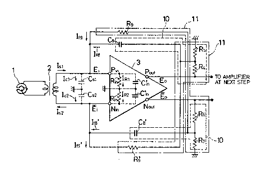
As showll in Fig. 1, a VTR for HDTV of the present
embodiment comprises a magnetic head 1, a rotary
transformer 2, and a magnetic reproducing head amplifier
3. In addition, the magnetic reproducing head amplifier 3
comprises a positive feedback circuit system 10 and a
negative feedback circuit system 11.
The magnetic head 1, which is secured, for example,
to a circumference surface of a rotary drum(not shown), is
built so that it may reproduce image signals recorded on a
magnetic recording medium such as a magnetlc tape, and
convert them into electric slgnals. The image signals
reproduced are entered to a negative phase input terminal
Nl~ and a positive phase input terminal Pl~ in the
magnetic reproducing head amplifier 3 functioning as a
differential amplifier through the rotary transformer 2
secured between the rotary drum and the fixed drum. The
magnetic reproducing head amplifier 3 is of a balanced
input type and also comprises a differential amplification
type IC of a balanced output type.
Between the positive phase input terminal Po~t of the
magnetic reproducing head amplifier 3 and ground, there
are connected dividing resistors R4 and R5 in series in
order from the side of the positive phase input terminal
Po~t. A connecting point between the dividing resistors
R4 and R, is connected to the positive phase input
~ - 14 -
201.Z969
terminal P1~ through a positive feedback capacitor ce.
The connectiny point between the dividing resistors R~ and
R, is also connected to the negative phase input terminal
Nl~ through a negative feedback resistor R9'. The
dividing resistors R4 and R5, and the positive feedback
capacitor C8 are circuit devices forming a positive
feedback circuit system 10. Similarly, the dividing
resistors R4 and R5, and the negative feedback resistor
R9' are circuit devices forming a negative feedback
circuit system 11.
Between the negative phase output terminal No~t of
the magnetic reproducing head amplifier 3 and ground,
there are connected dividing resistors R~ and R, in series
in order from the side of the terminal No~t. A connecting
point between the dividing resistors R6 and R, is
connected to the positive phase input terminal Pi~ through
a negative feedback resistor R9. The connecting point
between the dividing resistors R6 and R, is also connected
to the negative phase input terminal N1~ through a
positive feedback capacitor ce I . The dividing resistors
R~ and R,, and the positive feedback capacitor C~' are
circuit devices forming the positive feedback circuit
system 10. Similarly, the dividing resistors R~ and R"
and the negative feedback resistor R9 are circuit devices
forming the negative feedback circuit system 11. In
- 15 -
201Z969
addition, the positive phase output terminal Po~t and the
negative phase output terminal No~t are connected to the
input of an equalizer(not shown) through a reproducing
amplifier(next step amplifier) at the next step
downstream, which is not shown in the flgure.
The aforementioned dividing resistors R~ to R, are
installed so as to adjust a feedback amount from the
output according to an amplification factor of the
magnetic reproducing head amplifier 3, in the case where
the amplification factor is great. The positive feedback
capacitors C~ and C~'. are positive feedback devices, and
the negative feedback resistors Rg and Rg' are negative
feedback devices.
In the above configuration, voltages to ground for
the negative phase input terminal N1~ and the positive
phase input terminal Pi~ in the magnetic reproducing head
amplifier 3 are expressed as ~1 and E1 respectively.
Voltages to ground for the negative phase output~terminal
No~t and the positive phase output terminal Po~t are
expressed as Eo and Eo respectively. Moreover, stray
capacitances to ground(including the C'l~ = 2c1~ shown in
the figure as the reduced value for the input capacitance
C~ of the magnetic reproducing amplifier 3) for the
positive phase input terminal P1~ and the negative input
terminal N1~ in the magnetic reproducing head amplifier 3
- 16 -
2012969
are expressed as C~1 and C~2 respectively, and currents
pass through these are expressed as I~1 and I i2
respectively. In addition, there are current components
IR1 and IR2 passing through the input reslstors Ri~' s;
however the Inl and I~2 are small enough to be negligible.
Next, an explanation is given referring to the
operation of the magnetic reproducing head amplifier 3.
There is no essential difference in its operation between
the positive phase side and the negative phase side of the
magnetic reproducing head amplifier 3 except the reversed
polarity between those circuits. Therefore, the
explanation deals with the operation of the positive phase
side.
In the case where a signal, which is reproduced by
the magnetic head 1 and entered to the magnetic
reproducing amplifier 3 through the rotary transformer 2,
has a low frequency band, or where stray capacitances to
ground Col and C~2 in the magnetic reproducing head
amplifier 3 are small, a phase difference between an input
Ei at the positive phase input terminal Pi~ and an output
Eo at the positive phase output terminal Po~t iS
negligible, and therefore E1 and Eo are in the same phase
as shown in Fig. 3. In addition, a in Fig. 3 shows a
voltage dividing ratio concerning the dividing resistors
R4 and R~, and is also referred to as the voltage dividing
- 17 -
ZO~Z969
ratio concerning the dividing resistors R~ and R7(a =
R5/(R4 + R5) = R7/(R6 + R7)).
A charging current Ia1 flowing to the stray
capacitance to ground C~l is expressed as I
=j-2~-f-C~1-E1, and has a phase difference of 90 to E1 as
shown in Fig. 3. Moreover, a positive feedback current
I~, which is positively fed back to the input E1 through
a positive feedback capacitor C~, is expressed as I~8 =
j-2n-f-C8(aEO - E~), and has a phase difference of 90 to
Eo~ thereby being in the same phase as Icl.
Consequently, the charging current Icl to flow into
the stray capacitance to ground CA1 is mostly supplied
with the positive feedback current I~, and from a signal
source, only the differential current Ial between Icl and
Ir~ is supplied to the stray capacitance to ground C~l;
therefore the supply current to Crl from the signal source
may be reduced by a large margin. As a result, since an
effective capacitance becomes smaller, a resonance
frequency may be kept high.
The positive feedback current I~8 varies according to
a voltage obtained by dividing the output Eo by the
dividing resistors R4 and R5, and therefore by properly
selecting a dividing ratio as well as the value of C8 ~ a
compensation for the capacitance current I~l flowing to
the stray capacitance to ground COl may be appropriately
- 18 -
20129S9
achieved even in the case where the amplification factor
of the magnetic reproducing head amplifier 3 is great.
On the other hand, a current I~g, which passes
through the negative feedback resistor Rg from the output
Eo to the input Ei, has a negative phase to the input E1,
and functions to dump the resonance characteristic of the
input resonance circuit by its negative feedback
operation. By the use of the negatlve feedback current
I~g, which varies according to a voltage obtained by
dividing the output Eo by the dividing resistors R~ and
R,, the output amplitude characteristic of the magnetic
reproducing amplifier 3 is dumped as shown in a curve (N)
in Fig. 2. In addition, a curve (M) shows a frequency
characteristic of a gain which is obtained without using
the negative feedback.
In contrast to the above, in the case where the stray
capacitances to ground C~1 and COz(including the reduced
value for the amplifier input capacitance 2Cl~) in the
input part of the magnetic reproducing head amplifier 3
are great in transmitting a FM carrier with wide band, if
a feedback operation is not performed, a resonance
frequency in the resonance circuit formed by the stray
capacitances to ground Cn and C~2 as well as by the
inductance of the magnetic head 1 is reduced to fO', as
shown in a curve (K) in Fig. 2, and is shifted so as to
, _ -- 19 --
ZOlZ969
have its characteristic of the resonance frequency within
the FM carrier transmission band. In this case, if only a
negative feedback operation is applied, the output
amplitude characteristic of the magnetic reproducing
amplifier 3 is almost flattened because of the resonance
characteristic dumping as shown in a curve (L) in Fig. 2.
In the meantime, as to a high frequency band, the
output Eo of the magnetic reproducing head amplifier 3
sometimes has a phase delay to the input ~1 as shown in
Flg. 4. In the figure, a represents a dividing ratio
concerning the dividing resistors R~ and R, as well as R~
and R, similar to that shown in Fig. 3.
When such a phase delay as shown in the figure is
produced, a phase difference between the positive feedback
current I~A and the charging current Ic flowing to the
stray capacitance to ground COl doesn't come to 0, and
the current In1 which flows to the stray capacitance to
ground CO~ from the signal source is given as a vector
difference between IG~ and Ir~ as shown in Fig. 4. As a
result, the input E~ comes to contain a negative resistor
current component Io1~ besides a capacitance current
component I.1c. When the current component I~1~ becomes
greater than a current flowing to the input resistor R1~,
an oscillation is produced, and therefore the
amplification function for wide band of the magnetic
~ - 20 - 2012969
reproducing amplifier 3 fails to work well.
Hereupon, in order to eliminate the negative resistor
current component I~1~, the negative feedback current I r9
may be supplied to the positive phase input terminal Pln
from the output Eo of the negative phase output terminal
No~t through the negative feedback resistor R9, and
thereby a stable amplification function may be maintained
without having a CN ratio for the FM carrier reduced.
More specifically, since I~g = (a Eo - E1)/Rg is supplied
to the input Ei, the signal source current I~1 is changed
into I~l' as shown in Fig. 4, and thereby the negative
resistor current component becomes smaller.
Generally, a stable amplification function may not be
achieved only by the use of positive feedback, by
functioning a negative feedback as well as a positive
feedback at the same time, the resonance frequency fO may
be shifted to the vicinity of the upper limit of the FM
carrier transmission band as shown in a curve (M) in Fig.
2, and therefore the magnetic reproducing head amplifier 3
may perform its amplification operation for wide band in a
stable state. In addition, in the present embodiment, the
explanation was given referring to a magnetic reproducing
head amplifier for a magnetic recording/reproducing
apparatus, the present invention is generally applicable
to any case wherein signals with wide band have to be
~ - 21 -
2012969
amplified.
Next, referring to Fig. 5, another embodiment of the
present invention is described as follows. In addition,
the corresponding means are suffixed with the same
reference numerals and symbols in tlle aforementioned
embodiment for convenience, and a detailed explanation is
omitted.
In the configuration of the embodiment presented
here, as shown in Fig. 5, image signals reproduced by a
magnetic head 1 are entered to a magnetic reproducing head
amplifier 3 through a rotary transformer 2, and the
magnetic head amplifier 3 comprises differential
amplification type IC~ s of a balanced output type.
A negative phase input terminal N1~ of the magnetic
head amplifier 3 is connected to ground. However, in a
practical use, the negative input terminal N1~ is not
necessarily earthed, since the same effect may be achieved
without being earthed. A positive feedback device is
formed only by a positive feedback capacitor c~. The
positive feedback capacitor Ce iS connected between a
connecting point, at which dividing resistors R4 and Rs
are connected, and the positive phase input terminal Pl,..
Moreover, a negative feedback device is formed only by a
negative feedback resistor Rg. The negative feedback
resistor Rg is connected between a connecting point, at
- 22 -
2(~Z969
which dividing resistors R6 and R7 are connected, and the
positive phase input terminal P1~.
In the embodiment presented here, similar to the
aforementioned embodiment, positive and negative feedbacks
simultaneously made by the positive feedback capacitor C~
and the negative feedback resistor Rg enable the input
amplitude characteristic of the magnetic reproducing head
amplifier 3 to be flattened, and suitable for wide band.
Next, referring to Fig. 6, still another embodiment
of the present invention is described as follows. In
addition, the corresponding means are suffixed with the
same reference numerals and symbols for convenience in the
aforementioned embodiment, and a detailed explanation is
omitted.
In the configuration of the embodiment presented
here, as shown in Fig. 6, image signals reproduced by a
magnetic head 1 are entered to a magnetic reproducing head
amplifier 3 through a rotary transformer 2, and the
magnetic head amplifier 3 comprises differential
amplification type IC's of a balanced input type. A
negative phase output terminal No~t of the magnetic
reproducing head amplifier 3 is not installed, or is not
used even if it is installed. A positive feedback device
is formed only by a positive feedback capacitor C~. The
positive feedback capacitor C~ is connected between a
- 23 -
2012~;9
connecting point, at which dividing resistors Rq and R~
are connected, and a positive phase input terminal Pl~.
Moreover, a negative feedback device is formed only by a
negative feedback resistor Rg'. The resistor Rg' is
connected between a connecting point, at which dividing
reslstors R~ and R~ are connected, and a negative phase
input terminal Pl~.
Also in the embodiment presented here, similar to the
aforementioned embodiment, positive and negative feedbacks
simultaneously made by the positive feedback capacitor C~
and the negative feedback resistor R9' enable the input
amplitude characteristic of the magnetic reproducing head
amplifier 3 to be flattened, and suitable for wide band.
As is aforementioned, the magnetic reproduciny head
amplifier of the present invention has a configuration
wherein a positive feedback as well as a negative one is
simultaneously performed by adding the positive feedback
circuit and the negative one to its differential
amplifier.
According to the configuration, a resonance frequency
within a transmission frequency band may be shifted to the
vicinity of the upper limit of the frequency band by
utilizing the frequency characteristic of the magnetic
reproducing head amplifier. The reproducing equalizer may
obtain an amplitude equalization characteristic for its
~~ - 24 -
2012969
original purpose easily and stably. Besides, an inverted
compensation(a compensation by FM equalization) for a
resonance peak existing within the transmission frequency
band may be performed without overlapping each other with
the FM equalization performed by the equalizer, and
thereby required characteristics may be stably maintained.
Moreover, by making a turn ratlo in the rotary
transformer to have greater value, a CN ratio(carrier to
noise ratio) for the head amplifler output may be
improved.
The invention being thus described, it may be obvious
that the same may be varies in many ways. Such variations
are not to be regarded as a departure from the scope of
the invention.
There are described above novel features which the
skilled man will appreciate give rise to advantages.
These are each independent aspects of the invention to be
covered by the present application, irrespective of
whether or not they are included within the scope of the
following claims.