Note : Les descriptions sont présentées dans la langue officielle dans laquelle elles ont été soumises.
2 ~
- 1 -
LOW IMPEDANCE BUFFER CIRCUITl~
l~ield of Invention
This invention relates to amplifier circuitry and more particularly to
such circuitry having a iow output impedance.
5 Background of the Invention
Arnplifier circuitry having relatively low output impedance is necessary
for driving large capacitive or resistive loads, such as the relatively low impedance
of a telephone line, typically an impedance of about 600 ohms or less. In prior art,
such amplif~er circuitry typically is composed of a low impedance unity-gain buffer
10 output stage fed by one or more voltage-gain stages. This amplifier circuitrytypically is integrated in a semiconductor chip; whereas the load is situated off-chip.
For example, as shown in the textbook by P. R. Gray and R. G. Meyer,
Analysis and Desi~n of Analog Integrated Circuits (John Wiley & ~ons, second
edition, 198~) at page 759, Figure 12.43, a buffer stage for class B (push-pull) `
15 operation can be formed by a pair of error operational amplifiers (error op-amps)
which are connected to receive feedback from a pair of serially connected outputtransistors in such a manner as to assure unity voltage gain. The operation is class
AB (push-pull) in cases where in the quiescent (no signal) state both output
transistors conduct current, but one of them does not conduct any current whenever
20 the input voltage goes outside a narrow range, typically the range of about + 0.5 volt
around ground potential. As known in the art, class AB operation in general is
desirable from the standpoints of low standby power consumption and of no missing
output signals for small input signals (no "dead zone") which would distort the
output. Although such a buffer stage has the advantage of an output voltage swing
25 (range) which is fully rail-to-rail (e.g. power supply VDD to power supply Vss) and
the advantage of a low output impedance, it suffers from tlle disadvantage that any
inequality in the voltage offsets of the operational amplifiers results in an undesirable
non-conducting condition of one of the output transistors in the quiescent state,
whereby the desired (push-pull) class AB operation is not feasible. Also, the circuit
30 design is undesirably sensitive to semiconductor processing variations, so that either
excessive power dissipation or circuit instability (oscillations) caused by poorfeedback control over the quiescent current, or both, may result: Too high a
quiescent current is wasteful of power, whereas too low a quiescent current can
result in the above-mentioned circuit instability. That is, the circuit is not as reliable
35 or robust as is desired.
~. .
6~1
~ummary of the Invention
A more reliable or robust low impedance buffer stage, which can be
operated class AB, in accordance with the invention comprises:
(a) ISrst and second operational amplifiers each having an output
S terminal and a first and a second input terminal;
(b) first and second resistor nleans;
(c) first and second transistor devices respectively having first and
second relatively high-current-carrying controlled paths (source-drain paths) and
respectively having first and second relatively low current carrying control terminals;
(d) first and second power rails;
(e) first connection means for connecting, from the first power rail to the
second power rail, serially the first high-current path of the first transistor device, the
first resistor means, the second resistor means, and the second high-current path of
the second transistor device;
(f) second connection means for connecting a first node located between
the first transistor device and the first resistance means to the second input terminal
of the first operational amplifier;
(g) third connection means for connecting a second node located
between the second transistor device and the second resistance means to the second
20 input terminal of the second operational arnplifier; and
(h,~ fourth and fifth connection means for connecting respectively the
output terminal of the first operational amplifier and of the second operationalamplifier to the control terminal of the first transistor device and of the second
transistor device, respectively.
This buffer stage can advantageously be fed by a high voltage gain stage
of amplifier circuitry. Also, a pair of serially connected third and fourth transistors,
having much higher channel width-to-'ength ratios than the first and second
transistors, can be connected in parallel with the first and second transistors, in order
to make the output voltage swing more nearly approximate the rail-to-rail power
30 supply voltage. Furthermore, for full rail-to-rail output capability, a separate
switching transistor is inserted between the first and second rails, respectively, and
the first and second transistors; and each such switching transistor has its control
tern~inal respectively connected to the first and second nodes.
2 ~
Brief Descriplion of the Drawin~s
This invention, together with its features, advantages, and characteristics
may be better understood from the following detailed description when read in
conjunction with the drawing in which the FIGURE is a circuit schematic including
5 a buffer stage in amplifier circuitry.
Detail~d Description
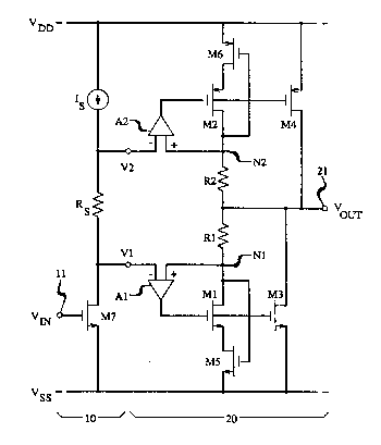
The FIGURE shows a low impedance buffer stage 20 in accordance
with the invention. Advantageously this buffer stage 20 is supplied with voltages ~1 -
and V2 by a high voltage gain stage 10. The circuitry of both the stages 10 and 20
10 can be integrated into a single silicon semiconductor chip, as known in the art and as
further discussed below.
In the FIGURE, power lines ("rails") VDD and ~rss are set at typically
+5 volt dc and -5 volt dc, respectively, as known in the art. A fixed electrical current
source of current Is is connected serially with a resistor Rs and an n-channel MOS
15 transistor M7 between the power rails, in order to form the high gain stage 10.
During operation, this high gain stage 10 receives an input voltage VIN at its input
terminal 11 and delivers voltages Vl and V2 to the buffer stage 20.
Each of a pair of standard op-amps Al and A2 (each of which can be
formed by a simple differential pair of transistors) is connected in the stage 20, and
20 each of these op-amps has its respective negative input terminal connected to receive
the voltages Vl and V2. Serially connected from rail to rail are n-channel MOS
transistors MS and Ml, a resistor Rl, a resistor R2, and p-channel transistors M2 and
M~. A node between the resistors Rl and R2 develops an output voltage VOUT at anoutp~t terminal 21 of the stage 20. Optionally, for reasons discussed below, another
25 n-channel MOS transistor M3 and another p-channel MOS transistor M4 are addedto the buffer stage 20 in parallel with the branch formed by the serially connected
M5, Ml, Rl, R2, M2 and M6. The transistors M3 and M4 are serially connected
from rail to rail. A node between these transistors M3 and M4iS connected to theoutput terminal 21.
Advantageously, the parameters of the transistors M3 and M4 are
selected so as to equalize their transconductances. The channel width to length ratio
(W/L) of each of M3 and M4 advantageously is at least about five times as large as
that of M1 and M2, respectively. Likewise, advantageously the transistors Ml andM2 are formed with equal transconductances. The resistors Rl and R2
35 advantageously are a matched pair (Rl=R2). The requirements of matched pairs for
Rl and R2, as well as for equal transconductances of M1 and M2,M3 and M4, need
--- 2 ~ 0 1
not be satisfied, at some penalty of signal distortion. Indeed, one of the resistances
Rl and R2 could be zero (short circuit).
The purpose of M5 and M6 is to enable full rail-to-rail output voltage
swing at the output terminal 21, for such full rail-to-rail operation tends to be
5 prevented by the voltage drop(s~ across Rl and R2. For example, because of thevoltage drop across R2, the output voltage VO~T cannot attain VDD regardless of
how high S12 rises, so long as current can flow through R2. In the presence of M6,
however, when V2 rises and causes the potentlal at the node N2 to rise to a threshold
below VDD, the transistor M6 turns off, whereby the voltage drop across R2 vanishes
10 and hence the transistor M4 can then bring the output voltage VOUT fully to VDD. If,
on the other hand, such full rail-to-rail output is not required, then the transistors M5
and M6 can be omitted, with the source terminals of Ml and M2, respectively, being
connected directly to vss and VDD-
Each of ~he op-amps Al and A2, respectively, has its output terminal
15 coupled (connected) to a low current carrying control terminal (gate terminal) of the
pair Ml, M3 and the pair M2, M4.
In practice, the op-amps Al and A2 are biased (not shown) so that there
is an adequate safety margin of non-zero quiescent current in a neighborhood of the
quiescent state (no signal region), in order to avoid the signal distortion problem
20 otherwise caused by a "dead zone" in which a change in the input signal would not
produce any change in the output.
The buffer stage 20 operates as follows. Because the op-amp Al and
A2, being operational amplifiers, cannot support any significant differences in the
voltages applied to their positive vs. negative input terminals, the feedback to their
25 positive input terminals supplied by node Nl located between Rl and Ml (to Al)
and by node N2 located between R2 and M2 (to A2) makes the quiescent current iQ
well-defined and controlled, i.e., adjustable to the desired value by proper selection
of parameters. More specifically, assuming that the source-drain voltage drop across
M5 and M6 are both m~lch less than a threshold of n-channel and p-channel
30 transistors, thé quiescent current iQ is given by:
iQ = Is Rs (l+a)/(Rl+R2) (1)
where the R's are the resistances of the respective designated resistors, and where a
is equal to the ratio of the width-to-length ratio (W/L)3 of M3 to that (W/L)l of Ml,
and equally of M4 to M2 (assuming matched pairs of transistors):
i~ 2~6~
a = (W/L)3 /(W/L)l = (W/L)4/(W/L)2 (2)
Note that from eq. (1) it follows the quiescent current iQ is thus well-
controllable and insensitive to semiconductor processing variations: the resistances
of the resistors track one another, as do the W/l, ratios. Although the current Is
5 supplied by the current source varies with semiconductor processing conditions, it
does so in a well-defined non-critical way, so that the quiescent current is relatively
stable with respect to variation in semiconductor processing conditions: the feedback
in the operational amplifiers does not introduce any significant circuit instability.
By selecting Rl=R2=R, then, in the quiescent state:
VOUT = (V1 +V2)/2; (3)
i.e., the output voltage of the buffer stage 20 then is conveniently equal to the
common mode voltage of the inputs Vl and V2 to this buffer stage.
As noted above, the transistors M3 and M4, as well as M6 and M5, can
be omitted, but then during class AB operation (push-pull) the output voltage VOI~T
15 could not swing as closely from VDD to Vss as it can when these transistors are
present. Note that the larger the value of a, as given by eq. (2), the closer the output
voltage swing becomes equal to rail to rail.
In order to assure stable operation with sufficient quiescent current, and
hence to assure class AB operation, Is and Rs should be selected to be large enough
20 to make ISRs greater than the sum of the maximum expected absolute values of the
operational amplifier offset voltages of Al and A2 by a factor of about 5 to about 10
or more, lest chip-to-chip variations of the offset in Al or A2 or both should cause
undesirably large chip-to-chip variations in the quiescent current iQ.
The resistors Rl, R2, Rs can be formed, for example, by standard
25 diffused regions in semiconductor or by standard deposited polysilicon resistors.
The current source Is can be formed by an MOS transistor biased in its saturation -
region, as known in the art.
Note that in the presence of signal applied to the gate terminal of M7,
the voltage drop (V2-Vl) across Rs remains fixed (Is Rs). That is, the difference
30 mode (V2 Vl)/2 is fixed; whereas the common mode (V2 + Vl)/2 varies with signal.
In a typical case, only by way of illustration, approximate values for the
various parameters are:
'.,', ~,~
--` 2~16~1
Rl = R2 = 2000 ohm; Rs = 1000 ohm; Is = 50 microamp;
a =30.
With signal, the output current at the output terminal 21 can go as high as 10
milliamp.
The gate terminal of M7, to which VIN is applied, can be connected, for
example, to the output terminal of a differential gain stage (not shown); and the
output terminal 21 of the stage 20 can then be connected, for the purpose of
feedback, to the negative input terminal of the differential gain stage. In that way,
overall unity gain of VOUT relative to the input voltage applied to a positive input
10 terminal of the differential gain stage can be achieved, in combination with overall ~`
high input impedance and low output impedance, as is desired in amplifier circuitry
for driving large currents into large loads (line drivers). ;~
Although the invention has been described in detail in terms of a
specific embodiment, various modifications can be made without departing from the
15 scope of the invention. For example, instead of n-channel and p-channel MOS
transistors, npn and pnp bipolar transistors can be used.