Note : Les descriptions sont présentées dans la langue officielle dans laquelle elles ont été soumises.
~0 17 179
''TITLE OF THE INVENTION
VIDEO SIGNAL DROP OUT COMPENSATION CIRCUIT
BACKGROUND OF THE INVENTION
Field of the Invention
The present invention relates to a video signal
playback system such as a video tape recorder and a video
disc player, and more particularly, to a drop out
compensation circuit to compensate lacking portions in
response to lack of video signals from a video head.
Description of the Background Art
Generally, a drop out compensation circuit
envelope-detects the FM reproduced output from a video
head, detects a portion where the envelope detected output
is lower than a predetermined level, and compensates the
low level portion with the FM reproduced output in the
immediate previous horizontal scanning period (hereinafter
referred to as "1H"). The video signal has line
correlativity and the gap of one horizontal scanning period
appearing on a screen has no effect on the human vision.
Such method of detecting a decrease in the envelope
level, however, responds to a level decrease of a long
duration such as a level decrease in high speed playback
and a level decrease in the first half or the latter half
of a field due to bad touching of a tape and a head.
Therefore, when the drop out compensation is performed by
20~7~~0
a drop out compensation circuit employing a 1H delay
circuit, as image signals for 1 H are used repeatedly
during the level decrease period, the pictorial image
becomes rather unnatural.
SUMMARY OF THE INVENTION
It is an object of this invention to provide a drop
out compensation circuit which can resolve the
unnaturalness of the pictorial image due to the drop out
compensation.
It is another object of this invention to provide a
drop out compensation circuit which does not perform the
drop out compensation longer than a predetermined period.
It is yet another object of this invention not to
vary the longest time period for performing the drop out
compensation in a drop out compensation circuit.
Briefly stated, a drop out compensation circuit in
accordance with this invention comprises an envelope
detecting circuit for envelope-detecting a reproduce
output from a «idee he~.d, a drop out detecting circuit for
detecting a level decrease of an envelope detected output,
a dela;r ~_=re~~i: f~~r d-ca~.ying the detected output of the
drop out detecting circuit by a predetermined time period,
a compensation period setting circuit, supplied with the
output of the delay circuit and the detected output of the
drop out detectioning circuit as inputs, for setting a
- 2 -
~Oi'~179
3rop out compensation period in response to the detected
output within the above predetermined time period, a one-
horizontal-period delay circuit for delaying the
reproduced output by one horizontal period, and a
selecting circuit for selecting a
one-horizontal-period-delayed reproduced output in
response to the output of the compensation period setting
circuit.
In operation, the reproduced output from the video
head is detected by the envelope detecting circuit. A
level decrease of the envelope-detected output is detected
by the drop out detecting circuit. The drop out detected
output is provided to the compensation period setting
circuit after delayed by a predetermined time period by
the delay circuit.
The compensation period setting circuit, in the case
where the drop out detected output lasts longer than a
predetermined period, does not provide signals for causing
the drop cut compensation to the video signal delay
circuit.
_A_r~Unr.~'~~;:lgly, ~I 4 d.~..71~.. Cut LviidltlOn iaStS lUIItjUI
than a predetermined time period, the drop out
compensation is not performed, so that the unnaturalness
of the pictorial image due to a long time drop out
25 compensation can be avoided.
- 3 -
20 17 179 -
Accordingly, in one of its aspects, the present
invention provides in a video signal reproducing
apparatus for reproducing video signals previously
recorded in a recording medium wherein said apparatus has
a video head, a drop out compensation circuit from
compensating for portions of decreased amplitude in a
reproduced output video signal produced from the video
head, said circuit comprising: means for envelope-
detecting said reproduced output video signal from the
video head and for producing a detected output signal
having a level corresponding to an amplitude of said
reproduced output video signal, means for producing a
drop out detection signal by comparing the level of said
detected output signal with a predetermined level, said
drop out detection signal having a pulse width
substantially equivalent to a duration of a level change
of said detected output signal, first means for delaying
the drop out detection signal by a prescribed time period
and producing a pulse signal, said pulse signal having a
pulse width commencing with a leading edge of said drop
out detection signal and terminating after said
prescribed time period, means, responsive to said drop
out detection signal and said pulse signal, for producing
a drop out compensation period signal by comparing the
pulse width of said drop out detection signal with the
- 3a -
~0 17 179 .
pulse width of said pulse signal, said drop out
compensation period signal having first and second states
and a duration equivalent to the shorter of either the
pulse width of the drop out detection signal or the pulse
width of the pulse signal, second means for delaying the
reproduced output video signal from the video head by one
horizontal period so as to form a one-horizontal period
delayed output video signal, and means, connected to said
reproduced output video signal and the one-horizontal
period delayed output video signal and operative in
response to said drop out compensation period signal, for
generating, in response to the first and second states of
the drop out compensation period signal, a drop out
compensated video signal as being either said reproduced
output video signal or said one-horizontal period delayed
output video signal, respectively.
In a further aspect, the present invention provides
in a video signal reproducing apparatus for reproducing
video signals previously recorded in a recording medium
wherein said apparatus has a video head, a drop out
compensation circuit for compensating for portions of
decreased amplitude in a reproduced output video signal
produced from the video head, said circuit comprising:
means for envelope-detecting said reproduced output video
signal from the video head and for producing a detected
- 3b -
~0 17179
output signal having a level corresponding to an
amplitude of said reproduced output video signal, means
for producing a drop out detection signal by comparing
the level of said detected output signal with a
predetermined level, said drop out detection signal
having a pulse width substantially equivalent to a
duration of a level change of said detected output
signal, first means for delaying the drop out detection
signal by a prescribed time period and producing a pulse
signal, said pulse signal having a pulse width commencing
with a leading edge of said drop out detection signal and
terminating after said prescribed time period, wherein
said first delaying means comprises: a constant-current
source for producing a constant current, a capacitor for
establishing said prescribed time period and provided
with a the drop out detection signal, a first transistor
having a base provided with a discharge current from said
capacitor and having an emitter providing the pulse
signal, a second transistor having a base provided with
said constant-current, and a current mirror circuit
having an input connected to a collector of said second
transistor and having an output connected to the emitter
of said first transistor, means, responsive to said drop
out detection signal and said pulse signal, for producing
a drop out compensation period signal by comparing the
- 3c -
~0 17 179 .
pulse width of said drop out detection signal with the
pulse width of said pulse signal, second states and a
duration equivalent to the shorter of either the pulse
width of the drop out detection signal or the pulse width
of the pulse signal, second means for delaying the
reproduced output video signal from the video head by one
horizontal period so as to form a one-horizontal period
delayed output video signal, and means, connected to said
reproduced output video signal and the one-horizontal
period delayed output video signal and operative in
response to said drop out compensation period signal, for
generating, in response to the first and second states of
the drop out compensation period signal, a drop out
compensated video signal as being either said reproduced
output video signal or said one-horizontal period delayed
output video signal, respectively.
- 3d -
~~.
2~~~1'~J
The foregoing and other objects, features, aspects
and advantages of the present invention will become more
apparent from the following detailed description of the
present invention when taken in conjunction with the
accompanying drawings.
BRIEF DESCRIPTION OF THE DRAWINGS
Fig. 1 is a block diagram showing one embodiment of a
drop out compensation circuit of this invention.
Fig. 2 is a characteristics diagram of a limiter
~Plifier.
Figs. 3 and 4 are waveform diagrams of waves of
respective parts of the drop out compensation circuit
shown in Fig. 1.
Fig. 5 is a block diagram showing another embodiment
of this invention.
Fig. 6 is a waveform diagram of waves of respective
parts of a drop out compensation circuit of the above Fig.
5.
Figs. 7 and 8 are circuit diagrams showing
modifications of delay circuits, respectively.
DESCRIPTIO?~t '.F I't.-1E PREFERnED EMBODIMEi~ITS
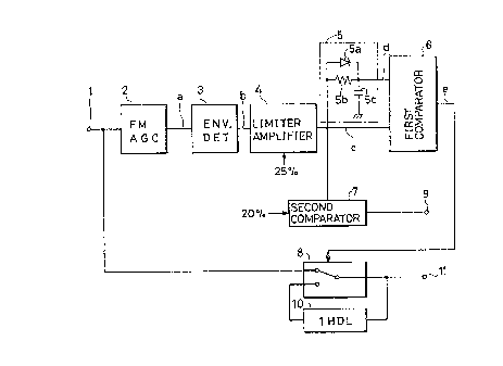
Fig. 1 is a block diagram showing one embodiment of a
drop out compensation circuit in accordance with this
invention.
- 4 -
~1~~'~9
Referring to the figure, a FM reproduced output is
provided to an input terminal 1 from a video head. An
FMAGC circuit 2 controls a gain to make the envelope level
of the reproduced output flat. An envelope detection
circuit 3 envelope-detects the FM reproduced output. A
limiter amplifier 4 (drop out detecting means) is a DC
amplifier provided with an amplitude limiting function,
which limits the envelope detected output to a fixed
level. This limiter amplifier 4 has input/output
characteristics shown in Fig. 2. When it is presumed that
the average envelope level after the automatic gain
control is 100, upon reception of an input of level
higher than about 25~, it is saturated and a H level is
provided. In the case of an input level lower than about
25$, an output proportional to the input is obtained.
A delay circuit 5 has a function for delaying the
fall of the output of the limiter amplifier 4 within a
range not exceeding 20 horizontal periods. Specifically,
it comprises an integrating circuit composed of a
capacitor 5c and a resistor 5b, and a diode 5a connected
to the resistor 5b in parallel, which provides a time
constant determined by the resistor 5b and the capacitor
5c upon the falling of the output of the limiter amplifier
4, and upon its rising, transmits the change quickly . As
the maximum delay period 20H is a period determined in
- 5 -
consideration of disorder of the pictorial image due to
the drop out compensation in one field, it is not limited
to be 20H. A first comparator 6 (compensation period
setting means) compares the output of the limiter
amplifier 4 and the output of the delay circuit 5, and
only when the level of the latter is higher than that of
the former, it provides a H level to a switch circuit 8.
A one-horizontal-period delay circuit 10 (referred to
as "a 1H delay circuit" hereinafter) delays the FM
reproduced output from the video head by one horizontal
period (1H).
The switch circuit 8 is responsive to the output of
the first comparator 6 to switch and connect the input
side thereof to the input terminal 1 or the 1H delay
circuit 10.
A second comparator 7 detects absence of FM reproduce
output and provides a no-signal detected signal to an
output terminal 9.
The operation of the drop out compensation circuit in
the above Fig. 1 will be described with reference to Figs.
3 an3 4.
In Figs. 3 and 4, time is illustrated on the axis of
abscissa and voltage is on the axis of ordinate, and Fig.
3 shows a case where the drop out period is shorter than
the maximum delay time, and Fig. 4 shows a case where the
- 6 -
~~'~~.'7~
drop out period is longer than the maximum delay time.
Figs. 3(a) and 4(a) are of a FM reproduced output of the
input terminal 1, Fig. 3 (b) is of the envelope detection
signal, Figs. 3(c) and 4(c) are of the drop out detection
signal, Figs. 3(d) and 4(d) are of the output signal of
the delay circuit 5, and Figs. 3(e) and 4(e) are of the
output signal a of the first comparator.
In case of a drop out of a relatively short period
due to dust on a tape or the like, the output c of the
limiter amplifier 4 varies as shown by the solid line in
Fig. 3(c). The output d of the delay circuit 5 varies
accordingly, as shown by the broken line. Thus, the
output a of the first comparator becomes a control signal
(high level) for causing the drop out compensation as
shown in Fig. 3(e). This high level control signal a is
provided to the switch circuit 8, and the switch circuit
8, in response to this, provides an 1H delay signal from
the 1H delay circuit 10 through the output terminal 11 to
an image circuit (not shown). The video signal lacking
portion is compensated by this 1H delay signal.
Or t::e ether hand, in case c~i air ou'cpu~. decrease of a
long period such as noise bar in high speed playback
(e. g., quintuplicated speed), the output c of the limiter
amplifier 4 and the output d of the delay circuit 5 vary
as shown by the solid line in Fig. 4(c) and the broken
line in Fig. 4(d), respectively. Accordingly, the output
a of the first comparator 6 varies as shown in Fig. 9(e),
and even if the level decrease period is long, the period
instructing the drop out compensation is within the
maximum delay period determined by the time constant of
the delay circuit 5.
That is to say, by causing the envelope detected
output b to become to vary in its state between two
values, H level and L level, by the limiter amplifier 4,
the determining operation of the first comparator 6 is
stabilized (as the level of the envelope detected output
varies). Meanwhile, as the envelope detected output b is
to be binary of high level and low level as described
above, a comparator can be used instead of the limiter
amplifier 4.
The second comparator 7 is provided with the
reference voltage of 20~ level as shown in Fig. 2, and
when the output c of the limiter amplifier 4 is lower than
this level, it provides a H level. Thus, by integrating
the output of the second comparator and discriminating the
level of the integrateu :salve, piese~~ee or absence or the
image signal can be determined. The screen is made
entirely black based on the no-signal determination
output.
_ g _
While the length of the period for the drop out
compensation is determined by the input level to the delay
circuit 5 and the time constant of the delay circuit 5, it
is decided to be about 20 horizontal periods in the
embodiment in consideration of the image disorder as
described above.
According to the invention described above, a drop
out compensation circuit which does not perform the drop
out compensation longer than the maximum delay period as
to a drop out of a long duration in high speed playback or
the like can be realized.
Fig. 5 is a block diagram showing a modification of
the delay circuit 5 and the first comparator in the above
Fig. 1.
Referring to the figure, the difference from Fig. 1
is that it employs a monostable multivibrator 12 as a
delay circuit 5, and an OR circuit 13 instead of the first
comparator.
The operation of the drop out compensation circuit in
the above Fig. 5 will be described in reference with the
-:a:~efox ; diug~~V,-r, of the Fig. 6 . Tiie ( cl ) and ( c2 ) of the
figure are of an output c of the limiter amplifier, (f) is
of an output f of the monostable multivibrator 12 and the
(gl) and (g2) are of the output g of the OR circuit 13.
- 9 -
~Q~~~~~
The drop out detected output c of the limiter
amplifier 4 is not only provided to the OR circuit 13
directly, but also is provided to the OR circuit 13 after
delayed by 20H periods by the monostable multivibrator 12.
When the low level period of the drop out detected
output c is shorter than the low level period of the delay
signal f (20H), the'signal itself becomes a control signal
g for the drop out~compensation during the drop out
detection period (refer to Figs. 6(cl), (f), and (gl)).
On the contrary, when the low level
period of the
drop out detected output c is longer than the low level
period of the delay signal f (20H), the delay signal f
(low level) becomes a control signal g in its output
period (refer to Fig. 6 (c2), (f), (g2)).
Accordingly, when the drop out period is longer than
20H, the drop out compensation can be surely stopped.
Fig. 7 is a circuit diagram showing a modification of
a delay circuit. Referring to the figure, upon
application ef a drop out detected signal to an input
tez°rainal 14, a capacitor 16 is charged by an input
transistor 15 ire a~:cc~rdan'e wi~.l: Said signal, and charged
voltage is provided to an output terminal 19 through an
output transistor 17. The discharging current of said
capacitor 16 flows to the base of the output transistor
17, so that the time constant can be changed by the base
- 10 -
20 17 17g .
current of said output transistor 17. Accordingly, by
employing the circuit of Fig. 7, the pulse width of the
drop out detected pulse can be changed.
Fig. 8 is a circuit diagram of an improved delay
circuit of the above Fig. 7.
Generally, hfe (current amplification factor) of a
transistor has a variation due to manufacturing process or
the like, especially when it is in an IC, for example, it
is considerable and the value can be doubled in some
cases. Referring to Fig. 7, it has a problem that the hfe
of the output transistor 17 changes to vary the base
current value, and the discharge time varies accordingly.
Referring to Fig. 8, the input transistor 20 is
provided with the drop out detected signal from an input
terminal 19. A first transistor 21 is provided with the
discharge current at the base thereof from a capacitor 22,
and provides a delay signal from an output terminal 23
connected to the emitter thereof. A constant-current
source 24 is a current mirror circuit comprising
transistors 24a and 24b. A second transistor 25 has its
base connected to said constant-current source 24 and its
collector connected to a first current mirror circuit 26.
The current ratio of the input side and the output side of
the first current mirror circuit 26 is 10:1. A second
current mirror circuit 27 has its input connected to the
- 11 -
~0 17 179
output of said first current mirror circuit 26 and its
output connected to the emitter of said first transistor
21, and the current ratio of the input side and the output
side is set to be 10:1.
Next, the operation will be described. When setting
the current f lowing to the transistor 24a of the
constant-current source to be 100IB, the current which is
equal to the current 100IB flows to the transistor 24b and
is provided to the base of the second transistor 25.
Then, the collector current of the second transistor 25
becomes 100hfe IB, and the collector current is inverted
by the first current mirror circuit 26 to become lOhfe IB,
and provided to the input of the second current mirror
circuit 27. Also, the current of lOhfe IB is inverted to
become hfe IB and the current hfe IB flows to the output.
The base current of the first transistor 21 at this time
is of a value found by dividing the emitter current of the
first transistor 21 (hfe IB) by the hfe of the first
transistor 21, that is, IB.
Accordingly, the base current of the first transistor
21 is not affected by the variation of the hfe of the
transistor, and can be determined according to the current
value of the constant-current source 14. Thus, it is
possible to take the output current of the second
transistor 25 having the same variation ratio as that of
- 12 -
YW '~a'
~,1Y
the hfe of the first transistor 21 as the emitter current,
and even if the hfe of the first transistor 21 varies, its
emitter current varies in the same direction and the base
current can be maintained at a predetermined value. Upon
manufacturing as ICs, transistors formed in a chip
generally have equal variation ratios. Therefore, the
circuit of Fig. 8 is especially suitable for manufactured
as an IC.
Next, a specific circuit constant of a drop out
compensation circuit will be described. The longest
operation time of a DOC circuit is set around 20H (H is
one horizontal period), which is about 1.27msec in time.
In Fig. 8, in consideration of manufacturing thereof as an
IC, when the maximum voltage of the output terminal 23 is
Presumed to be 2[V] and the capacitance of the capacitor
22 to be 50P [F], the discharge current I is found as
follows:
I = CV/T = 50 X 10 12 X 2/1.27 X 10 3 ~ 80nA
where; r = capacitance of the capacitor 11,
~~ V = r.he maximum voltage of the output terminal
ic. J ,
T = time until the discharge is completed.
To realize it in a circuit of Fig. 8, the current flowing
to the constant-current source 24 should be set at 8u[A].
- 13 -
As described above, according to the embodiment of
Fig. 8, when employing the base current of the transistor
as the discharge current of the charged capacitor, the
value of said base current can be maintained unchanged
regardless of the variation of hfe of the transistor.
Therefore, even when the drop out compensation circuit is
fabricated as an IC, the most suitable drop out
compensation operation time can be set.
The delay circuit of the embodiment of Fig. 8 can set
the delay time precisely in response to the pulse signal,
and can be applied to a variety of circuits which require
delay signals other than said drop out compensation
circuit.
Although the present invention has been described and
illustrated in detail, it is clearly understood that the
same is by way of illustration and example only and is not
to be taken by way of limitation, the spirit and scope of
the present invention being limited only by the terms of
the appended claims.
- 14 -