Note : Les descriptions sont présentées dans la langue officielle dans laquelle elles ont été soumises.
~ ~ ~ g ~
Title
CONNECTOR FOR CABL~ ~ONDUC~ORS
Field of the Invention
This invention relates to electric connectors and more
particularly to connectors Por cable conductors.
Description of the Prior ar_
~abla connectors are geneally known in the prior art. There
are basically two types oP such connectors. A first type, shown in
assignee'~ U.S. Patent 4,713,020 or in French patent specification
FR-A-2,56~,979 uses a contact element which Porms a spring-loaded
and pivotable wall, an end of which has an edge wh:Lch acts on the
conductor. With a conductor introduc~ed, the said wall is in contact
in its entirely with one side of the conductor. This construction,
however, takes up a relatively large amount oP space.
Furthermore in the connector according to the French patent
specification 2,566,967, the contack element is rigidly connected
to the base of the housing. However, this contact element does not
cooperate with the housing to provide contact with a conductor to
be introduced. The contact element according to the French patent
speciPication i9 A complicated part comprising several tongues
moving relative to ecah other. A ma~or drawback oP this device is
that it is very complicated and uses a lot of material~
; A second type prior art connector for cable conductors is
described in German patent specification DE-A-3,311,709 which
describes a connector havin~ a contact element with a pivotable
wall wherein the pivot point of the wall is positioned in the
direction of introduction o~ tha conductor beyond the point of
~` contact oP the conductor and wall. Such connectors are used in
applications wherein it is necessary to restrict the clamping
force of -the pivotable wall to the conductor~ This means that if a
2 2~3~
too large force is exerted on the conductor, it will slip through
the opening. This is important to prevent damage to the connector
or, if this connector is soldered to a printed circuit board
damage, to the circuit board. To release the conductors ~rom the
contact element, the housing according to this German patent
specification can be moved along a limited path relative to the
contact elements. By pushing the housing relative to the contact
element, the opening in the pivotable wall will be enlarged to
release the conductor. ~ecause of this, the contact elements have
to provide the support ~ace be~ween the conductor and a further
electric member, such as a printed circult board. To increase the
support ~ace accordirg to this prior art, each contact element is
U-shaped near the contact point with the board. Because of the
possibility of the movement of the housing relative to the contact
elements, it is necessary to take further steps to guarantee
contact between the conductor and the contact element. According to
the German patent specification, this is realized in that a set of
separate contact lips is provided on the contact element between
which the conductor has to be engaged. This further complicates the
contact element construction, I~ the connector hss several contact
elements, problems can also occur during introduction of a
conductor. Because the housing can tilt relative to the contact
elements, the openings in the housing might not align with the
opening in the contact elements. Furthermore, high locali~ed
pressure on the conductor will be directly trans~erred to the
nearest contact element and cause stress concentration on the
printed circuit board below. During introduction of the connector
with several contact elements in~o the printed circuit board,
problems can also arise because there is no guarantee that the
contact elements will all penetrate su~ficiently into the printed
circuit board during soldering. The same applies if, instead o~
soldering, a further connector is coupled to this connector.
~ecause of the complicated shape of this prior art connector, it is
not possible to produce the housing in one single step. Rather, it
becomes necessary to assembly the hous$ng ~rom at least two several
parts.
3 2 ~ 3
Summary oP the Invention
An object of this invention is to provide a connector having
several contact elements which ensures during introduction of the
connector into, for e~ample, a printed circuit board or orther
connector, guarantees that the contact elements all penetrate to
the same extent into the board or other connector. I~ a localized
force is exerted on the housing of the connector it must b~ equally
distributed over the base of the housing, which can have a
considerable area so that the underlying printed circuit board or
other connector is not harmed. Furthermore, tilting of the housing
during introduction of a multi-conductor wire is eliminated.
According to the invention, this and other objects are
realized with a connector having at least one contact element of
electrically conducting materlal for the clamping connection of an
electrical conductor. The connector comprises a housing having at
least one opening for introducing and removing the conductor, near
which opening the contact element is situated. The contact element
is provided with at least one spring-loaded and pivotable wall
having an aperture or opening with an edge for engaging the
conductor. This wall is so arranged that, when the conductor is
introduced, the wall is capable of pivoting in the direction of
freeing the opening and if the conductor moves outwardly, it is
capable of exerting a clamping Porce thereon against a wall of the
housing. The pivot point of the wall is positioned in the diraction
o~ introduction of the conductor beyond the point of contact of the
conductor and the wall. The contact element is rigidly connected
to the housing at the base o~ the housing. Because of the fixed
relationship of the lower part of the contact element to the
housing, its upper part comprising the pivotable wall can provide
in cooperation with the fixed wall of the housing sufficient
engagement with the conductor to obviate the need for further
contact lips to engage the conductor.
According to a prePerred embodiment of the invention, the
aperture in the pivotable wall is constructed as a slotted cutout.
In this way, the use oP material for the pivotable wall can be
limited as much as possible.
According to a further advantageous embodimènt, the contact
element comprises a single 3trip of conducting material of which
one extremity provides the pivotable wall and the other extremity
provides a connecting pin and is provided with means to engage the
housing. Because of the simple structure of the contact element, it
is possible to make the housing as one part, for example, by
injection molding. In the housing, no means are provided in the
housing to move the pivotable wall in such a direction that would
permit the conductor to be pulled back. This can be realized with
means in the wall for moving aside the spring-loaded and pivotable
wall to free the opening for a conductor~ These means can be either
separate me~ns which can be used for several connectors or cap
means constructed to be fitted over the housing of the connector at
theend with the opening for receiving the conductor and having at
least one corresponding opening and at least one device for
displacing the spring-loaded and pivotable wall.
To equally distribute the forces acting on several contact
elements provided in the connector, the contact element can be
disposed in a staggered arrangement. More contact elements can
thereby be arrnaged within the same area.
Brief description o~ the drawin~s
F~ure 1 shows diagrammaticallv in ~ide elevation a
connector according to the inventlon,
Figure 2 shows a section along the line II-II in Figure 1.
Figure 3 shows the connector according to Fig~lre 1 provided
with unlocking ~eans diagrammatically in side elevation, and
Figure 4 shows a section along the line IV-IV in Figure 3.
Detailed description of the Invention
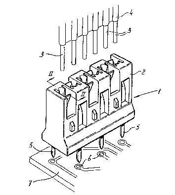
Figure 1 shows a connector indicated in its entirety by 1.
This comprises a connector housing 2 for receiving a row 4 of
conductors 3. The connector housing 2 is provided with contact
ends 5 to be fitted in openings 6 of an only partially shown
5 2 ~ 3
printed circuit board 7. As is clear from this Pigure contact ends
5 are placed in two opposed rows in a staggered arran~ement. This
allows furtber miniaturization.
Fi~ure 2 shows the connector housing 2 according to the
invention in section. In this, a conductor 3 is Pitted in the
opening intended therefor. A channel for receiving the conductor 3
comprises a fixed wall ô and a spring-loaded ~nd pivotable wall 9.
The spring-loaded and pivotable wall 9 comprises, in the exemplary
embodiment shown here, the extension o~ the contact end 5 and is
provided with an opening 12 or a cutout suitable for the same
purpose. Edge 10 of said opening 12 or cutout acts on the conductor
3-
In Figure 2 it is shown that near contact end 5 contact
element 25 is provided with recess 26 to engage a protrusion 27 in
the base of housing ~.
The device acts as ~ollows: when the conductor 3 is
inser~ed, the wall 9 moves outwards in the direction of the arrow
11, wlth the result that the conductor 3 is able to move along the
edge 10 through the opening 12 or cutout and arrives in the
position shown in Figure 2. As a result of the spring-loaded
action of the spring-loaded and pivotable wall in the direction of
arrow 13, the edge 10 is clamped against the conductor 3. If a
force is exerted on the conductor 3 iLn the direction of outward
movement of said conductor, the edge 10 will clamp into the
material oP the conductor 3, It is evident that the pivoting point
of the wall 9 is situated near the recelving part 14 of the
contact end 5. This is in contrast to the prior art, in which the
pivoting point is situated precisely at the other end of the
spring-loaded and pivotable wall 9, i.e. at the end where the
~0 conductor 3 is introduced into the connector. In the device
according to the prior art, this has the result that when a
tensile Porce is exerted on the conductor 3, the clamping force on
the spring-loaded and pivotable wall 9 becomes increasingly larger
with the risk ~P damage to, ~or example, the printed circuit board
7. Because the pivoting point o~ the spring-loaded and pivotable
wall 9 is sltuated, in the present invention, at the other side oP
the conductor near the receiving part 14, the clamping Porce
6 2 ~
exerted by the edge 10 will have certain limitsO These limits are
determined in particular, by the frictional force between the
different parts and the angle at which the wall 9 acts with its
edge 10 on the conductor 3.
Figure 3 shows the connector 1 according ~o Figures 1 and 2
which is provided with unlocking means 15 ~uch ~s a cap to be
fitted over the connector housing 2 and having corre~ponding
openings for introducing conductors 3. The operation of this
unlocking means 15 is evident from Figure 4, a section along the
line IV-IV in Figure 3. When the unlocking means 15 are pressed
in, lug 16 acts in the direction of arrow 17 on the end 18 of the
spring-loaded and pivotable wall 9 and this is moved outwards in
the direction of the arrow 11. Subsequently, the conductor 3 can
be introduced unhindered into the chRnnel intended therefor. After
the force on the unlocking means 15 is removed, the latter move
back upwards, with the result that the conductor 3 is clamped by
the movement of the spring-loaded and pivotable wall 9 in the
direction of the arrow 13. In order to prevent the un- locking
means 15 becoming detached from the connector housing 2, the
receiving part 14 and an end part 20 of the unlocking means 15 are
provided with snap means 21 which en~age in each other. The use of
the unlocking means 15 is of importance if it is intended to remove
the row 4 of conductors 3 after intrc)duction and if the conductors
3 are composed o~ a less rigid material, with the result that they
are unable to bend the spring-loaded and pivotable wall 9 aside
independently.
Although the ~nvention has been elucidated referring to a
embodiment being preferred to at the time being, it should be
understood that modifications can be made thereto without departing
from the scope of the present invention.