Note : Les descriptions sont présentées dans la langue officielle dans laquelle elles ont été soumises.
- 1 --
RD-19,680
CRYOGENI~ SEMICONDU~TO~ POWER
DEvICE$
The present invention relates to semiconductor
power devices and, more particularly, to novel solid-state
semiconductor power devices, such as metal-oxide-
semiconductor field-effect transistors (MOSFETs), static
induction transistors (SITs) and the like, for operation at
cryogenic temperatures, such as in a bath of liquid nitrogen
and the like coolants.
In many power generation applications, solid-stage
devices have replaced vacuum tubes. Due to the extremely
high power density which occurs in the very small volume of
most solid-state power devices (such as in the channel of a
MOSFET), the reliability and life of the device can be
shortened. While it is well known to minimize device power
dissipation by using switch-mode and other high-efficiency
methodologies, it is often difficult to provide for fast
removal of the heat energy generated inside the device, as by
dissipation of switching current in the on-resistance of a
power MOSFET. While good thermal design is required,
maximization of the thermal conductivity of the semiconductor
material, and the substrate upon which the device chip is
mounted, must be provided. A power device mounted and
packaged for operation at cryogenic temperatures, to provide
extremely high efficiency and very small size, is therefore
highly desirable.
B~ Summary ~ hQL-Ln~ontio~
In accordance with the invention, a solid-state
semiconductor power device optimized for cryogenic
applications has the actual device chip mounted on a
substrate of a material of very high thermal conductivity,
:
`
~ ~ ?~ a ~.,
RD-19,680
which is positioned in a bath of cryogenic fluid. The
substrate may be formed of beryllia, beryllium, alumina,
aluminum nitride, diamond and the like materials. The device
can be a MOSFET, SIT and the like.
A presently preferred embodiment has a substrate
disposed in a vertical plane, so that, if either or both of
the chip-mounting surface and the rear substrate surface are
bathed in the cryogenic cooling liquid, buildup of a low
thermal-conductivity vapor barrier between the cryogenic
liquid and the chip-supporting heat sink is prevented.
Accordingly, it is an object of the present
invention to provide novel cryogenic solid-state
semiconductor power devices for use in cryogenically-cooled
electronic assemblies.
This and other objects of the present invention
will become apparent upon reading of the following detailed
description, when considered in conjunction with the
associated drawings.
Brief De~cri~tion o~ the Drawin~
Figure 1 is a side view of a basic cryogenically-
cooled semiconductor power device, in accordance with the
principles of the present invention;
Figure 2 is a graph illustrating the thermal
conductivity of a number of materials, with respect to a
range of cryogenic and room temperatures;
Figure 3 is a sectional side view of one presently
preferred cryogenic semiconductor power device mounting
apparatus; and
Figure 4 ~s a schematic diagram of an equivalent
circuit of a MOSFET, and useful in appreciating aspects of
the present invention.
:
S'~
RD-19,680
~ çL ~5~2~iQn of the
Referring initially to Figure 1, a cryogenically-
coolable semiconductor power device 10 includes a heat sink
member 11 having a first surface lla upon which is mounted a
solid-state semiconductor power device chip 12, and having a
second surface llb which may be mounted upon a thermally-
conductive structural member 14, of copper and like material,
to hold the semiconductor chip 12 and supporting thermally-
conductive member 11 within a bath 15 of a cryogenic liquid,
such as liquid nitrogen (TN2) at a temperature of about 77-K.
In a device for use at room temperature, the heat sink
thickness T is made as small as possible, as the ~hermal
conductivity ~of the heat sink (say, BeO) is less than the
thermal conductivity of the member 14 material (say, Cu); at
cryogenic temperatures (say, 77-K) T is chosen to be much
larger, as ~eO iS greater than ~cu- Advantageously, device
10 is disposed in a vertical plane, i.e. with both surfaces
lla and llb vertically disposed, such that any vapor
thermally agitated from the surrounding cryogenic liquid mass
15 does not collect about the device 10 and form a low-
thermal-conductivity vapor barrier between device 10 and the
surrounding coolant device 15.
It is well known that the thermal conductivity of
some substrate materials, such as alumina, diamond, beryllia
and the like, tend to increase at cryogenic temperatures, and
in fact may peak near the temperature (i.e. 77-K) of liquid
nitrogen. The thermal conductivity of conductors such as
copper and aluminum and the like as well as of certain solid-
state-device-forming semiconductor materials (such as
silicon, germanium and the like) increase as temperatures are
decreased well into the cryogenic region. Tests of MOSFET
and SIT (static-induction-transistor) devices have shown that
many important electronic properties improve dramatically in
~ .
~ ~ f.~ " ~ t.~
RD-19,680
the cryogenic temperature regions. For example, the on-
resistance of high voltage (200-1000V) MOSFETs decreases by a
factor of between about 10 and about 30, at liquid nitrogen
temperatures, with respect to room temperature (e.g. 290-K).
The switching time, and therefore switching power loss,
decrease, as the effect of parasitic capacities decrease with
temperature. Therefore, speed increases, as well as
transconductance, gain and maximum current, due to increased
electron mobility. All such changes result in a lower-cost
device for handling the same power levels.
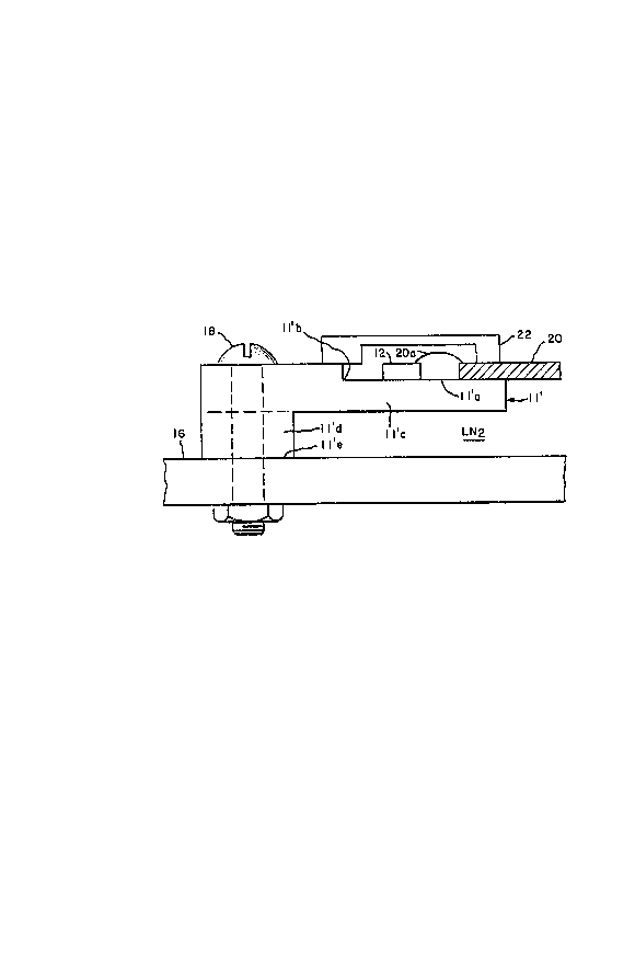
Another presently preferred apparatus 10' is shown
in Figure 3, wherein a generally L-shaped member 11' of a
high-thermal-conductivity, but electrically insulative,
material, such as aluminum nitride, beryllium oxide and the
like, has a first surface ll'a, which may be within a
recessed portion ll'b and the like, upon which the power
device die 12 is mounted. Recess ll'a is formed upon a leg
portion ll'c of the substrate, which also has a base portion
ll'd extending at right angles to leg portion ll'c, so that a
surface ll'e can be mounted against an insulative member 16.
Securing means 17, such as an insulated screw and the like,
can be utilized to fasten substrate 11' to member 16;
advantageously, member 16 may be vertlcally dlsposed, and
portion ll'd is a means for positioning the chip 12/substrate
ll'c such that a vapor barrier does not build up between the
coolant and the substrate. Alternatlvely, member 11' can be
made of an electrlcally and thermally conductive material,
such as beryllium, with member 16 being of a electrically-
insulative material; part of the member (i.e. leg ll'c) can
be of an electrically conductive material (Be) and another
part (portion ll'd) of an insulative material (BeO).
Electrical connections from device chip 12 to each of at
least one conductive leads 20 can be made by known means,
such as bonding wires 20a and the like. If desired, a cover
~ J~
RD-19,680
member 22 can be placed over the semiconductor die 12, to
provide additional protection thereto. In use, a cryogenic
agent, such as liquid nitrogen (LN2) and the like contacts at
least substrate 11', for withdrawal of dissipative thermal
energy from device 12, through the high thermal-conductivity
material of the supporting substrate.
Figure 4 is a schematic diagram illustrating the
actual elements of a real ~OSFET 12: in addition to an ideal
device 12l having an input capacitance Cin, an input
resistance Rin and a gate-drain capacitance Cgd, there is also
a parasitic bipolar transistor Qp, having its own base-
emitter parasitic resistance Rp and series-connected drain
capacitances Cdl and Cd2. Cryogenic cooling reduces the
undesirable effect of all of the parasitic elements, as well
as increasing the speed and maximum current handling
capability of device 12'.
While several presently preferred embodiments of
our novel invention have been described in detail herein,
many modifications and variations will now become apparent to
those skilled in the art. It is our intent, therefore, to be
limited only by the scope of the appending claims and not by
the specific details and instrumentalities presented by way
of explanation herein.