Note : Les descriptions sont présentées dans la langue officielle dans laquelle elles ont été soumises.
~c
-
2~24012
Y09-88-109 - 1 -
THERMOCOMPRESSION BONDING IN
INTEGRATED CIRCUIT PACKAGING
DESCRIPTION
Field of the Invention
The invention is in the field of electronic
packaging involving the providing of connecting leads
from densely packed circuit connection locations in an
integrated circuit chip to external circuitry.
Background of the Invention and
Relation to the Prior Art
The art generally employs a structure known as a
lead frame which spreads an array of leads, that are
closely spaced around an aperture in which the integrated
circuit chip is to be positioned, into an expanded and
more easily connectable spacing of the array, at the
periphery of the lead frame area. One illustration of a
lead frame type structure is shown in U.S. Patent
4,572,924.
There is an advantage in being able to join all
contacts simultaneously in a single operation. To
achieve this however all contacts should bond uniformly
under the same joining conditions.
The technique of thermocompression bonding, wherein
the heat in the bonding operation is accompanied by
pressure sufficient for plastic deformation of the parts
being bonded permits bonds to be made at lower
temperatures.
There are a number of factors that operate to narrow
the tolerances on the bonding conditions. Among them are
very small registration variations allowed between the
parts being bonded, lower heat tolerances arising from
more diffusion-sensitive and oxidation-sensitive
structures. This is particularly so for growth of
2~24~12
Y09-88-109 - 2 -
aluminum oxide on the aluminum alloys generally used.
Further, delamination of organic passivation layers
within the device is aggravated by an elevated
temperature.
The use of a slightly larger volume or bump of
material at a particular location is employed to assist
in registration and stress concentration in bonding. An
illustration of the use of such bumps is shown in U.S.
Patent 4,188,438.
As the art has continued to progress, a variation of
the lead frame technology has evolved in which a
conductor pattern is placed on a tape type filament
facilitating automated registration. This technology has
become known as Tape Automated Bonding (TAB). The
conductor lead ends are provided with bumps with the ends
extending as beam leads cantilevered into the opening for
the integrated circuit chip.
The TAB technology is described in the
"Microelectronics Packaging Handbook" edited by R.R.
Tummala and E.J. Rymaszewski, published by Van Nostrand,
(1989) pages 409-431. In the process of TAB bonding, as
the temperature is decreased, lower bond strengths are
encountered.
In IBM Technical Disclosure Bulletin, Vol. 30, No.
7, Dec. 1987, page 208, an improvement in
thermocompression bonds is reported with less compression
and shorter dwell time at the bonding temperature where
at least one of the bonding surfaces is roughened.
Further, in conventional fusion metallurgy, it has
been known that more reliable and uniform bonds can be
achieved where the lead end to be bonded is first
provided with a thin, fully-covering layer, and thereover
a thicker, bonding layer is then provided. The covering
layer is usually a non-oxidizing, preferably noble,
metal.
YO9-88-109 _ 3 _ 2~24012
One illustration of the technique is described in
U.S. patent 3,873,428 in which gold is used as
thecontacting material, and the different layers are
formed by plating, with a thicker gold layer being
produced.
Another illustration of the two layer fusion
contacting technique is described in French Patent
2,460,347 wherein the materials considered usable for the
layers are gold, silver and nickel, the layers are formed
by plating, but the difference in thickness between
plated layers is achieved by varying current density and
plating time.
" ,, . . , . ~
~-~ Summary of the Invention
The invention provides the interrelated structural
criteria with process steps and apparatus for the
production thereof, to enable the reliable use of the
thermocompression bonding technique, in densely packed,
multiple layer, integrated circuit packaging.
The contact member of the invention has, as an
intermediate manufacturing product, on the inner end of a
connecting member such as a beam lead of good conducting
material, a deformable layer of a metal taken from the
group of gold (Au), palladium (Pd), platinum (Pt), silver
(Ag), iridium (Ir) and nickel (Ni), of uniform texture,
free of dendritic protrusions, with a hardness value in
the range of that of soft gold which is approximately 90
on the Knoop scale, with a rough surface morphology of
ridges with a modulation frequency from peak to peak of
approximately 1 micrometer and with a depth between
ridges in the range of 1/4 to 1/2 of the average
integrated circuit pad depth.
The intermediate manufacturing product contact
member with the uniform, rough-surfaced, deformable
bonding layer forms a thermocompression bond to an
external connection pad that is approximately
micrometer thick on an integrated circuit at a
Y09-~8-109 - 4 - 2 02 40 1 2
temperature of 500C~or less, and the contact from the
conducting member to the pad is approximately 2
micrometers thick. The invention allows the temperature
and/or the bonding force at which reliable bonds are
made, to be reduced.
The deformable layer, free of dendritic protrusions,
with the rough surface morphology is producible by
electroplating under higher than normal electronegative
conditions. One example of such conditions is the use of
a voltage range between 2.0 and 3.0 volts from cathode to
anode within a range of current density from 0.03
milliamperes per s~. cm. to 0.05 milliamperes per sq.
cm., for a standard pure metal plating bath of the
neutral cyanide type used in the semiconductor industry,
as described in thé Metal Finishing Guidebook, Vol. 83,
No. lA, in an article entitled "Gold Plating" by A.M.
Weisberg, Metals & Plastics Pub. Inc., Hackensack, N.J.,
1985.
_
Plating apparatus employing multiple anodes provides
increased control insuring uniformity of the rough
surface thick deformable metal layer on different area
surfaces.
Brief Description of the Drawings
Figure 1 is a photomicrograph of the
thermocompression bondable contact member of the
invention.
Figure 2 is a high magnification photomicrograph of
the surface morphology of the thermocompression bondable
contact member of the invention.
Figure 3 is a schematic - view of the
thermocompression bondable contact member of the
invention showing the interrelationship of periodicity
and depth of ridges to pad thickness.
2024012
Y09-88-109 _ 5 _
Figure 4 is a top plan view of the lead frame type
of packaging with which the invention provides
fabrication advantages.
Figures 5 to 9 are cross sectional views of
thermocompression bonded conductor and integrated circuit
contact structures and apparatus in accordance with the
invention.
Figure 10 is a photomicrograph of a prior art type
plated gold contact.
Figure 11 is a high magnification photomicrograph of
a prior art type plated gold contact illustrating the
surface morphology thereof.
. .
---Figures 12 and 13 are photomicrographs of the
-~ contact of the invention at different magnifications
illustrating a reduced roughness surface morphology.
Figures 14 and 15 are photomicrographs of a contact
where the bond layer contains dendritic type hard
inclusions that produce an inferior bond.
Figures 16 and 17 are photomicrographs of the cross
section of the contact of the invention at an aluminum
pad silicon integrated chip interface at 500C and 350C
bonding temperatures, respectively.
Description of the Invention
In the technology of thermocompression bonding, a
comhination of heat and press~re is applied across a
contact interface having as one portion thereof a
deformable layer so that under the pressure the plastic
deformation of that layer operates to bring the interface
to the bonding temperature more quickly and to enhance
diffusion. The result is that strong and reliable bonds
are formed with less temperature.
~ .
2Q2~
Y09-88-109 - 6 -
When, however, the sizes are reduced to where the
contact is of the order of 100 micrometers wide and the
spacing between contacts is of the order of 100
micrometers, a number of interdependent aspects require
consideration. The deformable layer must provide the
requisite electrical properties, it must deform at an
essentially uniform pressure from contact to contact,
there must be enough material in the deformable layer and
a proper surface on the deformable layer so that a full
contact interface is formed.
In accordance with the invention, it has been found
that the technique of thermocompression bonding can be
employed in densely packed integrated circuits where:
the connecting member, such as a beam lead, is covered
with a uniform layer of deformable metal in the contact
area; the deformable metal layer has a hardness value in
the range of that of soft gold which is on the Knoop
scale approximately 90; a thickness in the range of 0.3
to 1.3 micrometers and a surface morphology that is rough
with ridges with a modulation frequency of approximately
1 micrometer from peak to peak and a depth of about 1/4
to 1/2 the thickness of the average integrated circuit
pad. The 1 micrometer roughness is about half the total
thickness of the contact after bonding, which is about 2
micrometers.
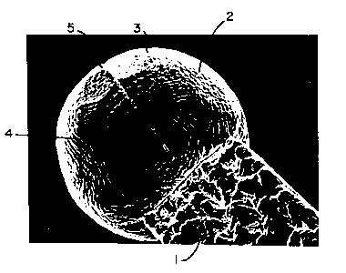
Referring to Figure 1, a photomicrograph, a
preferred embodiment of the contact member of the
invention, is shown, wherein on a copper base or lead end
1, a contact surface 2 is covered with a deformable layer
3 of soft gold with a Knoop hardness of up to
approximately 90 and a thickness in the range from 0.3 to
1.3 micrometers and with a rough surface morphology in
the form of ridges 4 with a modulation frequency of
approximately 1 micrometer, that is from ridge peak to
peak and a depth between peaks of approximately 1/4 to
1/2 the thickness of the pad to which the end 1 is to be
thermocompression bonded.
2024012
Y09-88-109 - 7 _
The size of the contact in Figure 1 is approximately
100 micrometers across. The spherical or bump end on the
lead or conductor 1 is usually produced by laser melting
of the conductor 1 tip. The deformable metal is then
formed thereover, preferable in two layers. A first,
thin covering layer of a non-oxidizing or noble metal of,
for example, gold, silver, platinum or nickel is applied,
and thereover, the soft uniform texture deformable layer
with the rough surface morphology, such as in the pure
gold embodiment of Figure 1, is applied. The deformable
layer is the only one visible in the figure and is
identified as element 3.
Referring next to Figure 2, the preferred embodiment
of the invention shown in Figure 1 is shown at higher
magnification to more clearly accentuate the detail of
the deformable layer roughness of the surface morphology.
The ridges 4 on the surface are separated from peak to
peak by about 1 micrometer which thereby provides a
periodicity of about 1 micrometer, and the depth between
the ridges 4 is approximately 1/4 to 1/2 of the thickness
of the integrated circuit pad to which it is to be
bonded. At present densities, the average integrated
circuit pad thickness is about 1 micrometer.
The deformable layer 3 is nearly uniform in
thickness over the contact surface 2.
The roughness produced by the ridges 4 is about half
the thickness of the bond when the contact is formed.
Referring next to Figure 3, there is shown a
schematic cross sectional view of the thermocompression
bondable contact member in contact with the pad on the
chip before the thermocompression bonding operation. In
Figure 3, on a chip 6, a pad or bump 7, surrounded by
passivation 8, extends essentially vertically from the
surface of the chip 6 a distance or thickness A which may
be small as 1 micrometer in high density technologies.
The ridges 4, having a periodicity, shown as dimension B,
are in contact with the surface 9 of the pad 7. The
-
2024012
Y09-88-109 - 8 -
depth of the ridges 4 is shown as dimension C and is
approximately 1/4 to 1/2 of the minimum pad thickness
dimension A.
In accordance with the invention, the rough surface
morphology of the layer 3, free of dendritic protrusions
is formed on the contact surface 2 by plating a metal
taken from the group of Au, Pd, Pt, Ag, Ir and Ni under
special conditions. In general, the plating is performed
under greater than normal electronegative conditions.
The electronegative conditions in a plating bath may be
influenced by the makeup of the bath and by the
electrical conditions of operation.
Where the bath is a standard pure metal bath
containing a salt of the metal being plated at a pH of
about 6 operated at a temperature that is slightly
elevated, a voltage range between 2.0 and 3.0 volts from
cathode to anode at a current density range of 0.2 to 0.6
milliamperes per square centimeter will produce
satisfactory electronegative conditions.
In accordance with the invention, there is a current
density range of about a factor of three above which
dendritic protrusions appear that are detrimental to the
contact.
There is listed in Table 1 typical plating solutions
for metals in addition to gold which are usable for the
deformable layer.
202~012
Y09-88-109 - 9 -
TABLE 1
Metal Solution
Pd Palladous Chloride or
Palladous Phosphate
Pt Alkaline Platimate or
Chloroplatenic Acid
Ag Silver Cyanide
Ir Hydrated Iridium Dioxide
Ni Nickel Sulfate or
Nickel Chloride
Referring to Figure 4, there is shown a top plan
view of a typical lead frame type packaging member used
in the art with which the invention provides advantages.
In Figure 4, the lead frame spreads an array of beam
leads that are closely spaced around an aperture 10,
under which the integrated circuit chip, shown dotted, is
to be positioned, into an expanded and more easily
connectable spacing of the array, at the periphery 11.
The lead frame technology, where convenient, employs
vertical spacing elements 15. Thus, while the example
lead frame of Figure 4 is shown in a plan two-dimensional
view, in fact, as the art was developing, a third and
multiple dimensions in the use of lead frames in stacked
arrays are being employed in the packaging field.
Communication between vertically stacked conductor
elements has heretofore in the art been handled by via
type connections passing through the insulation
separating the conductors but the laying down of
conductors requires a certain amount of lateral tolerance
and tolerances can add up to misregistration. ,As is
illustrated with this lead frame, a step in the art has
been made by providing beam lead cantilevered portions 13
of the conductors extending into the aperture lO so that
conductor interconnections can be made in the same type
2024012
Y09-88-109 - 10 -
of operation as the bonding to the pads on a chip that is
positioned under the opening 10. Further, as the art has
developed, it has been found that the applying of the
lead frame to an insulating backing having sprocket-like
holes 14 on the edges permits the lead frame packaging to
be handled similar to that of an ordinary film and
brought into registration with the chip, providing
thereby the tape automated bonding technology in the art.
It will be apparent to one skilled in the art that
as the vertical and interconductor spacing becomes
tighter and tighter, the criteria connected with the
invention that all simultaneously thermally compressed
contacts respond in deformation essentially uniformly and
do so at the very lowest possible temperature becomes of
increasing value. Further, as the spacing is becoming
smaller, the number of contacts may also increase in
order to keep reactance effects from limiting signal
transmission. This increase occurs because more ground
and power conductors and ground planes are being
introduc2d into the packaging which in turn adds to the
number and density of connections.
In Figures 5 through 9, structural illustrations are
provided of the connecting capability made possible by
the invention in permitting the use of thermocompression
bonding. As the spacing becomes tighter and tighter, it
is of advantage to be able to precisely position the
connection between two conductors on either side of an
insulating backing. Referring to Figures 5, 6 and 7, the
insulator is the element 15 with the conductors 16 and 17-
in Figure 5, 20 and 21 in Figure 6 and 24 and 25 in
Figure 7, being on opposite sides of the insulator and in
Figure 5, conductors 16 and 17 are connected at
connection 18 and similar connection 19 in the same plane
or at the same surface of the insulator 15 as the
conductor 16. In Figure 6, connections 22 and 23 are
positioned intermediate in the thickness of the insulator
15 so that both the conductors 20 and 21 bend slightly
down to the connection and in Figure 7 the connections 26
and 27 are formed on the same plane as the conductor 25.
2~24012
Y09-88-109 - 11 -
, .. --
Since the invention accommodates the technique of
thermocompression bonding then the conductors will be
held in position during the application of the
compression force and consequently the tooling that
retains the members of the contact in position during
bonding can be positioned with respect to the insulator
15 so that the connection can be anywhere in the vertical
distance between the conductors. When it is considered
that the minimum thickness for the insulator is generally
of the order of the conductor spacing, as the density in
packing becomes greater, the capability to produce these
structures becomes of greater importance.
Referring next to Figures 8 and 9, there are shown
illustrations, respectively, of a single and a double
chip attachment in the opening 10. In Figure 8,
conductors 26 and 28 cantilever over the opening 10 on
one side of the insulator 15 and conductors 27 and 29
cantilever over the opening 10 on the other side of the
insulator 15. The chip, with two schematic connections
30 and 31 each representing a pad on the chip 32, is
positio~ed in a compression force and thermal heat cycle
applying tool, shown schematically as 33 with an opposing
tool 34, so that on applying force and temperature
between elements 33 and 34 the conductors 26 to 29 bend
into contact with the bonding pads and are compressively
bonded to the chip.
Referring next to Figure 9, the principles of Figure
8 are then extended to the two-sided type chip in which,
in essence, two chips are positioned and bonded in
parallel. The structure in Figure 9 is shown after the
bonding has taken place. In Figure 9, conductors ~6 and
37 are on opposite faces of the insulator 15 on on side
of the opening 10 and conductors 35 and 38 are on
opposite faces of the insulator 15 on the other side of
the opening 10. The chip 44 has illustrative pads 41 and
42 and the chip 43 has illustrative pads 39 and 40. With
the use of tooling of the type employed in Figure 8 in
which both temperature and compression are applied, the
bonds 45 and 46 are thermocompressively formed, with the
~;
2024012
Y09-88-109 - 12 -
pads 39, 41, and conductor 37 forming a bond at 45 and
the pads 40, 42 and conductor 35 forming a bond at 46.
It will be apparent to one skilled in the art that with
the invention substantial circuit interconnection becomes
possible with a single thermocompressive bonding
operation.
The contact member of the invention, as illustrated
in connection with Figure 1, may be compared with the
type of contact standard in the prior art as illustrated
in Figures 10 and 11.
Referring to Figure 10, in the prior art the end of
a copper lead is made in the shape of a ball by laser
melting over which is placed a plated gold layer
estimated to be in the vicinity of 0.5 to 0.8 micrometers
thick. The morphology of the prior art contact surface
is relatively smooth. This fact is focused on in the
enlarged view in Figure 11. In accordance with the
invention, the contact of the invention differs from the
prior art of Figures 10 and 11, first by the fact that
the plating of the deformable layer is thicker, ranging
from 0.3 to 3.0 micrometers, thereby insuring sufficient
deformable material appropriate for the individually
varying bonding conditions associated with many
simultaneous bonds. Second, the plating is controlled to
be soft, with a hardness limitation in that the hardness
should not greatly exceed that of soft gold which is
approximately 90 on the Knoop scale. Third, the surface
morphology, rather than being smooth as in Figures 10 and
11, is rough with a periodicity of about one micrometer
between ridges and having a depth of about 1/4 to 1/2 the
thickness of the average integrated circuit pad. Fourth,
the deformable layer texture is controlled to be uniform
throughout, being free of dendritic protrusions.
In accordance with the invention, the preferred
embodiment rough surface pure gold deformable bonding
layer can be produced by plating in a standard pure
conditions of 2.5 volts between cathode and anode and
with a current density ranging from 0.03 milliamperes per
202~012
Y09-88-109 - 13 -
square centimeter to 0.05 milliamperes per square
centimeter. Standard pure gold plating baths are well
known in the art. In general, they contain a salt of
the gold in a solution with a pH of about 6 and are
operated at a temperature of about 65C. As
illustrations, for perspective, normal pure gold plating
baths are employed as baths "C", "D", "E" and "F", in an
article entitled "The Strength and Ductility of Some Gold
Electrodeposits" by J.M. Deuber and G.R. Lurie, pages 715
to 719, July 1973, in Plating Magazine, and in the Metal
Finishing Guidebook published by Metals & Plastics
Publications, Hackensack, N.J., 1985, in an article by
A.M. Weisberg on pages 232-234, the neutral cyanide type
solution baths used by the semiconductor industry are
described.
Further, in accordance with the invention, the
uniform soft gold deformable layer of the contact of the
invention can be produced by plating within a high but
defined range of current densities.
Referring to Figures 12 and 13, photomicrographs of
the contact of the invention are shown where the lower or
minimum current density of 0.02 milliamperes per square
centimeter was employed. As may be seen in Figure 12 and
in the higher resolution of Figure 13, the surface
morphology at this stage clearly shows the periodicity
and depth of the ridges but those ridges are not as
pronounced as those shown in Figures 1 and 2. They are,
however, adequate for all but the most stringent
specification bonding operations. The other extreme in
the high but defined current density range is illustrated
in Figures 14 and 15 wherein the plating took place at
roughly greater than three times the current density of
Figures 12 and 13 or 0.075 milliamperes per square
centimeter. In Figure 14, and then in the higher
resolution 15, spots in the surface indicate the
beginning of dendritic protrusions. The dendritic
protrusions cause the deformable layer to be non-uniform,
which interferes with the plastic flow of the deformable
layer and in turn may cause unsatisfactory and unreliable
-
202~012
Y09-88-109 - 14 -
bonds. Thus, there is a narrow range of current
densitie~ over about a factor of 3 in which the
thermocompressive bond contact of the invention can be
plated.
The contact of the invention is of particular
advantage in making a thermocompression bond to a silicon
type chip with many contact metallurgies including
aluminum and its alloys.
Referring next to Figures 16 and 17, cross sectional
photomicrographs of the contact of the invention are
shown of Al chip contact pads at different temperatures.
The scale illustrates that the thickness of the
intermetallic regions of the contact corresponds to,about
twice the 1 micrometer roughness measure of the contact
member surface before bonding.
A thermocompression bond is shown first at 500 C in
Eigure 16 and then at 350 C in Figure 17. As the
temperature is reduced and approaches the 350C level,
the bond strength is lowered but is still within a
satisfactory level. This is a primary advantage of the
invention wherein bonding temperatures may be reduced.
It should be noted in comparison between Figures 16 and
17 that the thickness of the layer of gold/gold-aluminum
intermetallic is greater at the higher temperature bond
illustrating that the thermocompression bonding
technology available through the invention, with its
attendant lower temperature capability, is particularly
beneficial in joining to silicon chips.
One of the unique aspects of the lead frame
technology wherein connections are bonded in the opening
for the chip thereby permitting the use of both sides of
the dielectric for conductors is that plating, as is
illustrated with the structures in Figures 5 to 9, may
involve sides with different areas so that to insure
uniformity over the entire surface greater control is
desirable. In Figures 5 to 9 where one side is a ground
plane, a continuous sheet of metal may be employed
202~Q12
Y09-88-109 - 15 -
producing a substantial difference in area to be plated.
In accordance with the invention, the plating bath
apparatu~ lS modified to provide each different area side
with an independent anode which in turn is supplied by an
independent power source so that different
electronegative conditions may be established during
plating and a uniform plated layer achieved independent
of area.
Best Mode for Carryinq Out the Invention
The thermocompressively bondable contact of the
invention as illustrated in Figure 1 is fabricated using
a copper lead member on which there is a first covering
plating of pure gold at 0.01 milliamperes per square
centimeter for 5 minutes, followed at 2.5 volts~ by a
second plated layer at a higher current density of 0.03
to 0.05 milliamperes per square centimeter for 5 minutes.
The hardness of the second pure gold layer is
approximately 90 on the Knoop scale and the thickness is
approximately one micrometer produced by plating at 0.03
milliamperes per square centimeter in a standard pure
gold plating bath having separate anodes for each area
side, each separated by a voltage range between 2.0 and
3.0 volts from a particular conductor area.
What has been described is a thermocompressively
bondable contact for integrated circuit packaging and the
manufacturing technology therefor which provides lower
fusion temperature and more reliable contacts. It is to
be understood that the various embodiments are simply
illustrative of the principles of the invention and that
modifications and changes may readily be envisioned by
those skilled in the art in the light of the principles
set forth.