Note : Les descriptions sont présentées dans la langue officielle dans laquelle elles ont été soumises.
UNIFORM CURRENT ANL) VOLTAGE DISTRIBUTTON DEVICE
BACKGROUND
The present invention relates in general to
voltage and current distribution devices, and more par
ticularly to such devices which are capable of uniformly
distributing current and voltage to a plurality of indi
vidual electrical circuit components.
Uniform or balances distribution of current and
voltage is desirable in a variety of situations. One
such situation involves transient voltage surge suppres-
sor systems, wherein unequal power loading of multiple
surge suppression components reduces the effectiveness of
the system, and causes excessive stress on the more heav-
ily loaded components, which results in premature failure
of those componewts. However, prior surge suppression
systems have not provided for uniform distribution of
current and voltage to the individual components making
up the system. For example, U.S. Patent No. 4,635,160 to
Riley discloses a transient voltage suppression assembly
wherein each of a plurality of voltage suppression
devices (VSDs' mounted on a grounded conductor plate is
connected to a separate conductor extending through the
assembly. Riley is concerned only with minimizing the
parasitic inductance of each VSD, and no provision is
made for providing a common voltage/current to the plural
VSDs.
Another electrical protector assembly is dis-
closed in U.S. Patent No. 3,917,982 to George et al. In
the George et al. device, plural protective devices are
maLtnted in longitudinally spaced sections of the assem-
bly, and a shunt lead of each protective device is con~
netted to a ground bus member extending beneath the
protective devices. Consequently, the various protective
dwices have unequal. circuit paths to ground.
SUMMARY OF THE INVENTION
It is therefore an object of the invention to
provide a device which is capable of uniformly distribut-
ing current and voltage to a plurality of electrical
circuit components.
It is another ob ject of the invention to pro
vide a uniform current and voltage distribution device
which is easily and economically manufactured, reliable,
rugged and easily maintained,
xt is a still further ob ject of the invention
to provide a uniform current and voltage distribution
device which is compatible with a wide range of possible
applications and circuit components, including but not
limited to transient voltage surge suppression.
These and other objects and advantages are
achieved in accordance with the present invention by a
uniform current and voltage distribution device which
includes first and second terminals, a first electrical
1S bus electrically connected to the first terminal, a
second electrical bus electrically isolated from the
first electrical bus and electrically connected to the
second terminal, and a plurality of electrical components
connected between the first and second buses so as to
form a plurality of circuit paths of equal length, each
circuit path running between the first terminal, the
first electrical bus, one of the circuit components, the
second electrical bus, and the second terminal.
In accordance with another aspect of the inven
Lion, the plurality of electrical components are con~
nected to the first and second buses at locations which
are equidistant from the first and second terminals,
respectively.
In accordance with yet another aspect of 'the
invention, in one embodiment the first terminal is part
of the first bus, the second terminal is part of the
second bus, the fixst and second buses are respectively
disposed on separate first and second planar support
members which are joined together in facing relationship,
and the first support member has two sets of apertures,
one set communicating with the first bus for permitting
connection of one of the leads of each circuit component
~~~~~~9
- 3 -
to a respective one of the connection locations on the
first bus, and the second set of aperture permitting
another of the leads of each circuit component to extend
through the first support member for connection to the
second bus.
In accordance with yet another aspect of the
invention, in a second embodiment, the first bus com-
prises a first conductive member disposed on a support
member, and the second bus comprises an annular second
conductive member disposed on the same support member
around the first conductive member and concentric there-
with.
These and other features and advantages of the
invention are described in or are apparent from the fol-
lowing detailed description of the preferred embodiments.
BRIEF DEaCRIPTTON OF THE DRAWING
The preferred embodiments axe described with
reference to the drawing in which:
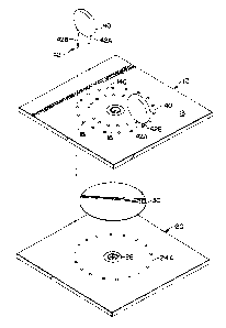
Fig. 1 is an exploded perspective view of a
first embodiment of a uniform current and voltage dis~tri
bution device constructed in accordance with the present
invention .
Figs. 2 and 3 axe respectively plan views of
the bottom faces of portions of the embodiment of Fig. 1.
Fig. 4 is a plan view of a portion of a second
embodiment of a uniform current and voltage distribution
device constructed in accordance with the present inven-
tion;
Fig. 5 is an elevation view of the embodiment
of Fig. 4, with a partial cross-section taken along the
line 5-5 of Fig. 4; and
Fig. 6 is an elevation view, partly cut away,
of a 'third embodiment of the present invention.
DESCRIPTION OF THE PREFERRED FAMBODL~IENTS
Referring to Figs. 1-~, a first embodimeazt of a
uniform current and voltage distribution device con-
structed in accordance with the present invention
- 4 _
comprises first and second electrically non-conductive
support members 10 and 20, an intermediate insulator
member 30 disposed therebetween and a plurality of elec-
trical circuit components 40 mounted on support members
10 and 20 in the manner described in more detail herein-
after. As shown, support members 10 and 20 preferably
have a substantially planar, plate-like configuration,
and are made from standard epoxy-glass printed circuit
board material. Advantageously, one of the members 10,
20 can be an integral part of a larger printed circuit
board containing other components. As shown, peripheral
mounting holes 15 and 25 advantageously are respectively
provided in support members 10 and 20 for physically
securing the support members together with mechanical
connectors (not shown). Alternatively, an adhesive or
the like can be used to secure the support members.
Support members 10 and 20 have formed on their
respective bottom faces 12 and 22 electrically conductive
bus members 14 and 24 which include terminal members 16
and 26 for connection to conductors (not shown). Bus
members 14 and 24 advantageously are layers of conductive
material formed on the respective support members 10 and
20 by conventional printed circuit techniques. As shown,
(Fig. 3) bus member 14 preferably has a spoke configura-
tion comprising a central circular portion 14A and plu-
rality of radially extending spokes 14B of equal length
which each terminates in a connecting aperture 14C
extending through support member 10. Spokes 14B advan-
tageously are dimensioned so as to function as fuses
having a predetermined current rating which "blow" when
the current passing through bus member 14 exceeds the
rating limit. 2t will be appreciated that bus member 14
alternatively may have a circular or other geometric
configuration which does not include spokes. As shown,
terminal member 16 is disposed at the center of bus mem-
ber 14 and advantageously is in the form of a circular
aperture in support member 10 to facilitate connection of
- 5 -
a conductor thereto.
As shown (Fig. 2), bus member 24 preferably has
a circular configuration with terminal 26 formed at the
center thereof, and a ring of apertures 24A concentric
with terminal. 26 extending through support member 20.
Terminal 26 advantageously has the same circular aperture
farm as terminal 16.
As shown, support member 10 includes a further
ring of apertures 18 concentric with terminal 16 and
having the same diameter and circumferential spacing of
the apertures as the ring of apertures 24A on support
member 20. Further, apertures 14C of bus member 14 are
respectively radially aligned with corresponding ones of
apertures 18, and the difference between the radius of
the ring formed by apertures 14C and the radius of the
rings of apertures 18 and 24A corresponds to the spacing
between the connecting leads 42 of electrical circuit
components 40. Tnsulator member 30 preferably has a
circular configuration, as shown, with a radius greater
than that of the ring of apertures 14C but less than that
of the rings of apertures 28 and 24A.
As shown, electrical circuit components 40,
which may be any type of circuit component, for example,
a voltage surge suppression device such as a metal oxide
varistor (MOV) or the like, are mounted on the top face
13 of support member Z0. One lead 42A of each circuit
component 40 extends through one of the apertures 14C of
bus rnembex 14 and is electrically joined, e.g., by sol-
dering or the like, to the associated spoke 14B of bus
member 14. The other lead 42B of each circuit component
extends through the associated aligned aperture g8 of
support member 10, and through aperture 24A in support
member ?.0, and is electrically connected to bus member
24. It will be appreciated that the present invention
35 can be used with mufti-lead Circuit components having
more than two heads. For example, two of the leads of
such a component may be connected to the respective bus
~Q~~
members in the manner shown, with the additional leads
connected either to further bus members or to individual
circuit conductors as desired.
It will be appreciated by those of ordinary
skill in the art from the foregoing that a plurality of
circuit paths of equal length are formed running between
terminal 16, bus member 14, each circuit component 40,
bus member 24, and terminal 26, so that voltage and cur
rent applied to either terminal can be equally distri
buted 'to the plurality of circuit components.
Referring now to Figs. 4 and 5, a second embod-
iment of a uniform current and voltage distribution
device constructed in accordance with the present
invention will now be described. As shown, the second
embodiment comprises a generally circular electrically
conductive member 50 and an annular electrically conduc-
tive member 60 coaxially mounted on an electrically non-
conductive substrate 70. Similarly to the first
embodiment described hereinabove, substrate 70 is made
from standard printed circuit board material and can be
an integral part of a larger printed circuit board con-
taining other components. In addition, conductive
members 50 and 60 similarly advantageously are conductive
layers formed on substrate 70 by conventional printed
circuit techniques. An electrically conductive, substan-
tially cylindrical cap member 80 extending above sub-
strate 70 is electrically connected at its flanged rim 82
to an outer periphery of the annular member 60 by
soldering or other conventional means. Cap member 80
includes a top portion 84, with optional vent holes 86,
which preferably is formed as an integral part of cap
member 80, as shown, but which may be separately formed
and electrically connected to the vertical wall 83 of cap
member 80.
.~s shown, conductive member 50 has the same
configuration as bus member I4 in the first embodiment,
and accordingly will not be described in detail other
_ 7 _
than to note that a conductor 90 in the form of a
threaded rod is shown in Fig. 5 mounted in the connecting
terminal aperture 56 and secured and electrically con-
nected to conductive member 50 by means of two nuts 92
disposed on opposite sides of substrate 70. Conductive
member 60 has a ring of apertures 62 extending through
substrate 70. Similarly to the first embodiment, aper-
tures 62 are radially aligned with corresponding ones of
the apertures 50C formed in conductive member 50, and the
difference in the respective radii of the two rings of
apertures corresponds to the spacing between the leads 42
of the electrical components 40 connected between the
conductive members. Preferably, as shown, the ring of
apertures 62 is formed at the inner periphery of conduc
tive member 60.
Cap member 80 also has a centrally located
connecting terminal 86 in the form of a circular aperture
which is preferably coaxially aligned with terminal aper-
ture 56 of conductive member 50. A conductor 94 similar
to conductor 90 is also shown mounted to terminal 86 and
electrically connected to cap member 80 by -two nuts 96 in
the same fashion as conductor 90.
Similarly to the first embodiment, one lead 42A
of each circuit component 40 extends through one of the
apertures 50C and is electrically joined, e.g., by sol
dering or the like, to the associated spoke 50B of con«
ductive ember 50; and the other lead 42B of each circuit
component 40 extends through the associated aligned aper-
~ture 62 and is similarly electrically connected to con-
ductive member 60. Tt will be appreciated that while
circuit components 40 are shown as depending from the
bottom face of substrate 70, they may also be mounted so
as to project from the top face of substrate 70 and to be
housed within cap member 80. Tt will also be
appreciated that conductive members 50 and 60 can
alternatively be provided with connecting pins or nodules
(not shown) to which the circuit component leads are
~~P~
attached.
As is apparent from the foregoing, conductive
member 50 of the present embodiment corresponds in func-
tion to bus member 14 of the first embodiment, while
conductive member 60 and cap member 80 together corre-
spond to bus member 24. Hence, as in the first embodi-
ment, the second embodiment provides a plurality of
circuit paths of equal length, running between terminal
86, cap member 80, conductive member 60, each circuit
component 40, conductive member 50 and terminal 56, so
that voltage and current applied to either terminal can
be equally distributed to the plurality of circuit
components.
As alternative embodiment of the present inven
tion is depicted in Fig. 6. This embadimer~t is identical
to the second embodiment depicted in Figs. 4 and 5,
except that cap member 80 includes a threaded portion. 87
at its distal end for engagement with a mating hole 96 in
a plate form of conductor 94, such that the engaging
periphery of cap member constitutes the connecting
terminal 86' . Of course, cap member 80 in this emboli-
ment may also be electrically connected to conductor
plate 94 is soldering or other convewti~rnal means in lieu
of the threaded connection, or may be integrally formed
as part of a conductor.
It will be appreciated from the foregoing that
the exceptionally simple design of the uniform current
and voltage distribution devices of the present invention
is readily and economically manufactured, and provides a
rugged anal reliable device. The present invention is
pa~ti.cularly adapted to provide uniform current and volt-
age distribution to more than two electrical com-
ponents. However, the number of circuit components 40
which may be utilized with the present invention is
determined from the requirements of a specif~.c applica~
Lion. Thus, although embodiments have been illustrated
which permit a maximum of eighteen components, it will be
fully appreciated from the above disclosure that the
device may be configured to provide for uniform distri-
bution of current and voltage through any number of com-
ponents. (It is noted that laboratory tests performed on
transient voltage suppression assemblies constructed with
eighteen metal oxide varistors serving as the circuit
components demonstrated safe accommodation of typical
loads in varying quantities through 100kA within a time
period of 50 ~s. )
It will be appreciated from the foregoing that
the present invention is not limited to embodiments in
which the connection locations on the respective bus
members for the circuit component leads have a circular
arrangement, or are equidistantly spaced from each other,
or are symmetrically disposed with respect to the corre-
sponding terminals of the uniform current and voltage
distribution device.
Many other applications of the uniform current
and voltage distribution device of the present invention
will be apparent to those of ordinary skill in the art
from the foregoing disclosure. In addition, many modifi-
cations and variations to the disclosed uniform current
and voltage distribution devices are possible in light of
the above teachings. It is to be understood that, within
the scope of 'the appended claims, the invention may b2
practiced otherwise then as specifically shown and
described without departing from the spirit and scope of
the invention.