Note : Les descriptions sont présentées dans la langue officielle dans laquelle elles ont été soumises.
203332S
D E S C R I P T I O N
SUPERCONDUCTING WIRE AND METHOD OF MANUFACTURING
THE SAME
TECHNICAL FI~LD
The present invention relates to a superconducting
wire used for a superconducting electromagnet and a
method of manufacturing the superconducting wire.
BACKGROUND ART
In recent years, superconducting wires made of
various materials have remarkably been put to practical
use. To advance the practical use of such wires, it is
important to increase the amount of electric current,
which can flow through the wires, that is, to increase
the critical current density (Jc).
One method of increasing Jc is increasing the
pinning force for capturing magnetic flux in a
superconducting wire within a magnetic field produced by
a coil of the superconducting wire, which magnetic flux
enters the superconducting wire. This method is called
"pin stop", and a portion having the pin stop effect is
termed "pinning center."
In the prior art, an alloy superconducting wire is
sub,jected to heat treatment at the time of final wire
drawing, and a normal conducting deposited portion or
2033325
-- 2
strained portion, produced through the heat treatment, is
employed as a pinning center.
It is known that a pinning center in a compound
superconducting wire is normally present at a grain
boundary. The pinning center in the compound
superconducting wire may be explained, for example, with
reference to a manufacturing method illustrated in Figs.
5A to 5E. An Nb or Nb alloy ingot 41, as shown in Fig.
5A, is buried in a bronze (containing Sn) pipe 42, as
shown in Fig. 5B. The resultant structure is processed
into a hexagonal wire element 43 (see Fig. 5C~.
Subsequently, as is shown in Fig. 5D, a plurality of wire
elements 43 are gathered and buried in a bronze
(containing Sn) pipe 44. After the resultant structure
is subjected to wire drawing, as illustrated in Fig. 5E,
it is thermally treated to produce an intermetallic
compound layer (Nb3Sn layer), thus obtaining a
superconducting wire. The intermetallic compound of the
superconducting wire is a polycrystal. A cross-sectional
structure of the polycrystal is shown, for example, in
Fig. 5F. That is, there are crystal grains 45 of Nb3Sn
and grain boundaries 46.
In order to enhance the Jc of the above compound
superconducting wire, it is generally practiced to
control parameters such as the size, density and
contamination of the grain boundaries, thereby
introducing strong pinning points. Conventionally, these
Z033325
-- 3
parameters are controlled by varying the temperature and
time for heat treatment or adding a third substance, such
as Ta, Ti, Hf or Ga in a Nb core or a matrix to make the
grain boundaries dirty.
Regarding an alloy superconducting wire, in order to
make pinning centers function effectively to enhance the
pin stop effect, it is important to appropriately
determine the size and arrangement of the pinning
centers. Where the pinning centers are introduced by
heat treatment or by utilizing process strain, it is very
difficult to suitably control the sizes of normal
conducting deposited portions and strained portions and
the distance therebetween. Further, when the wire is
finally processed, heat treatment must be repeated
several times. Consequently, manufacturing time
increases and also the number of manufacturing steps
increases.
Where grain boundaries are employed as pinning
centers in the compound superconducting wire, a pinning
force Fp and an applied magnetic field B have the
relationship:
Fp ~ ~l-B/Bc)
where Bc: critical magnetic field.
As the intensity of the applied magnetic field
approaches that of the critical magnetic field, the
pinning force decreases suddenly and Jc decreases at high
magnetic field, which is disadvantageous.
2033325
-- 4
The present lnventlon has been made ln conslderatlon of the
above clrcumstances and lts ob~ect ls to provlde a
superconductlng wlre made of varlous superconductlng
substances and havlng enhanced pln stop effect and Jc, and to
provlde a method of manufacturlng the superconductlng wire.
DISCLOSURE OF THE INVENTION
According to a flrst broad aspect, the inventlon
provldes a superconductlng wire having an elongated filament
comprlslng a plurality of elongated superconducting wlre
elements, sald superconductlng wlre elements each belng made
of an alloy-based superconductlng substance and said
superconductlng wlre elements each lncludlng a plnnlng center
made of at least one wlre of a non-superconductlng substance
buried in said alloy-based superconducting substance and
extendlng in the longitudinal direction of said fllament,
characterized ln that sald at least one wlre of non-
superconductlng substance has a dlameter greater than or equal
to 7 nm and less than 500 nm.
The alloy based superconductlng wlre can be
manufactured by a method comprlsing the s-teps of: burying a
wire of non-superconducting substance in the longltudlnal
dlrection of the superconductlng wlre; gathering a plurality
of superconducting wlre elements ln which the non-
superconductlng wires were burled; drawlng the gathered wlre
elements lnto a fllament; and gatherlng a plurallty of sald
72465-21
2033325
-- 5
fllaments and reducing the dlameter of the resultant
structure. Also, the alloy-based superconductlng wlre can be
manufactured by a method comprislng the steps of burylng a
plurallty of wlres of non-superconductlng substance ln the
longltudlnal dlrectlon of the superconductlng wlre; reduclng
the dlameter of the resultant structure to obtaln a fllament;
and gatherlng a plurality of the filaments and reducing the
diameter of the resultant body.
Accordlng to thls method, lt ls possible to freely
control, at the deslgn stage, the slze, type, shape, dlstance
and posltlon of the pinnlng center of non-superconductlng
substance introduced into the fllament, ln accordance wlth the
use of the wlre, e.g. the intensity of magnetlc field. Thus,
the matching wlth the lattlce of magnetlc flux can be enhanced
and the elemental plnnlng force can be effectlvely exhlblted
and lncreased, whereby Jc can be greatly lmproved. Besldes,
since no heat treatment ls performed, the manufacturing tlme
and cost can be reduced.
In the above alloy-reduclng super conductlng wlre,
it ls deslrable that the alloy whlch forms the alloy-based
supercoducting wlre element be a publlcly known
superconductlng substance, e.g. NbTl alloy.
It ls deslrable that the non-superconductlng
substance for formlng the plnnlng center be Cu or a Cu alloy;
Cu or a Cu alloy coated wlth Nb or Ta; Cu or a Cu alloy mlxed
wlth 0.5 to 5 % by welght of magnetlc substance; Cu or a Cu
alloy coated wlth Nb or Ta and mlxed wlth 0.1 to 5 % by welght
1~-
72465-21
2033325
-- 6
of magnetlc substance; a preclous metal such as Ag or Au, or
an alloy thereof; or a preclous metal such as Ag or Au, or an
alloy thereof, whlch is mixed wlth 0.5 to 5% by welght of
magnetlc substance.
BRIEF DESCRIPTION OF THE DRAWINGS
Figs. lA to lD lllustrate a method of manufacturlng
a superconductlng wlre accordlng to Example l;
Flg. 2 ls a flowchart lllustratlng a manufacturlng
method accordlng to Example 3;
Flgs. 3A to 3D lllustrate a method of manufacturlng
a superconducting wire according to Example 4;
Flgs. 4A to 4E lllustrate a method of manufacturing
a superconducting wlre according to Example 5; and
Flgs. 5A to 5F lllustrate a conventlonal method of
manufacturing a compound superconductlng wlre.
BEST MODES OF THE INVENTION
Example 1
", , ~.
72465-21
2033325
-- 7
The outer periphery of a Cu rod having a diameter of
3 mm was coated with a Nb sheet. The Cu rod was inserted
into a through hole formed in a central part of a NbTi
alloy wire having a diameter of 35 mm. A plurality of
NbTi alloy wires were inserted into a Cu billet having a
diameter of 453 mm. Thereafter, the Cu billet was hot-
e~ciuded at 700 ~C and drawn (the billet was removed
during drawing), thus obtainin~ a superconducting wire
element 1 of NbTi alloy having a hexagonal final cross
section and a distance of 1.83 mm between parallel sides.
In this case, the Cu rod serves as a pinning center, as
will be described below.
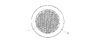
As is shown in Fig. lA, 253 superconducting wire
elements 1 were gathered and inserted into a Cu-10% Ni
alloy billet 2 having its outer peripheral surface coated
with Nb and having a diameter of 453 mm. The resultant
body was hot-e~truded at ~C and the diameter thereof was
reduced, thus obtaining a secondary wire element
(filament) 3 having a he~agonal final cross section and a
distance of 3.15 mm between parallel sides (see Fig. lB).
The secondary wire element 3 is a composite of a number
of superconducting wire elements 1.
Then, as is shown in Fi~ lB, 151 filaments 3 were
gathered and inserted into a Cu billet 4 having a
diameter of 453 mm. The resultant body was hot-extruded
at 600 ~C and the diameter thereof was reduced, thus
obtaining a tertiary wire element 5 having a hexagonal
72465-21
- 8 - 2033325
final cross section and a distance of 2.6 mm between
parallel sides (see Fig. lC). The tertiary wire element
5 is a composite of a number of secondary wire elements
3.
The 241 tertiary wire elements ~ were gathered and
buried in a CU billet 6 having a diameter of ~53 mm, as
shown in Fig. lC. The resultant structure was hot-
e.-~truded at 600 ~C and the diameter thereof was reduced,
thus obtaining a superconducting wire 7 having a diameter
of 10 mm or less. If the cross section of each
superconducting wire element 1 constituting the
superconducting wire 7, it is found that a Cu pinning
center 9 coated with a Nb sheet is present at the center
of a he~agonal NbTi alloy 8 ~see Fig. lD).
For e~ample, when the superconducting wire 7 had the
diameter of 0.2 mm, the diameter of the filament 3 was
0.507 ~m, the diameter of the pinning center 9 was 3.7
nm, and the distance between adjacent pinning centers 9
was 30 nm.
Current densities were measured with respect to the
above-stated superconducting wire having Cu pinning
centers, a superconducting wire manufactured in like
manner with pinning centers of Ag-30 wt% Pd alloy, and a
superconducting wire of a NbTi alloy in which pinning
centers were introduced by a conventional heat treatment
method. The results are shown in Table 1.
72465-21
o o
Table l
superconduct- No Type of Pins Treatment Fila~(ent Pin Size Pln D nsity J C(A/cllr ) at 5 T
Wire of this 1 C U No 0.1 0. 1 l 3 4 x 10 5 1. 9 x 10 3
Wire of this 2 C u No 0.5 5 10 7,2 X 10⁵ 3. l x l 0 5
Wire of this 3 C u No 1 lO 15 9.6 X 10⁵ 4,7 X 10⁵
invent ion
invention 4 C u No 10 1000 50 3. 1 x 10 5 2,1 X 10⁵
invention 5 C U No 100 10000 50 2.1 X 10⁵ 1.1 X 10⁵
invention 6Ag - 30w t %P d No 0.1 0.1 1 3 7 X 10⁵ 2.0 X 10⁵
Wiire ~i this 7 Ag-30wt%Pd No 0.5 7 12 9.1 X 10³ 4. 3 x lo6
invention 8Ag -30wt %P d No 1 10 15 9.8 X 10⁵ 5,0 X 10⁵
Wire of this g Ag-30wt%Pd No 10 1000 50 3. 2x 10⁵ 2. 3x 10⁵
invention
Wire of this 10 Ag-30wt%Pd No 100 10000 50 2,2 X 10⁵ 1. 3x 10⁵ r~
inventlon
Conventional 11 a - T i Yes 1 Not Measured Not Measurec 6.5 X 10⁵ 2,2 X 10⁵ ~'~
Coinventi~nal 12 No 1 4.1 X 10~ 2.5 X 10~ r~
o~
~ Note: The pin density indicates the percentage (%) of pins in the filament.
' ~ - lO- 2033325
As is seen from Table 1, any of the superconducting
wires according to the present Example has a Jc
remarkably higher than that of conventional
superconducting wire No. 12. The wires Nos. 2, 3, 7 and
8 have higher Jc than conventional wire No. 11. These
results seem to have stemmed from the improved matching
between the magnetic lattice and the size, position, etc.
of the pinning center and also the enhanced pin stop
effect.
Example 2
First, 8~ holes, each having a diameter of 2 mm,
were formed in a NbTi ingot with a diameter of 40 mm.
Then, a Cu rod, which will become a pinning center, was
inserted into each hole. The resultant structure was
buried in a Cu pipe with an outside diameter of 4~ mm.
The resultant body was hot-extruded and drawn into a
primary wire element having a diameter of 2 mm. Then,
the outer Cu pipe was dissolved away by nitric acid.
The 100 primary wire elements were put in a CuNi
pipe having an outer diameter of 45 mm. The resultant
body was hot-extruded and drawn into a secondary wire
element with a diameter of 2 mm.
The 250 secondary wire elements were put in a Cu
pipe with an outside diameter of ~7 mm. The resultant
body was hydrostatic-extruded and drawn, thereby
obtaining a superconducting wire. The diameter of the Cu
pinning center in the superconducting wire was 100 nm.7246s_
2033325
-- 11 --
The superconducting wire was rolled into a tape-like
material, so that the cross section of the pinning center
was made to have an oval shape. The current densities Jc
of the thus obtained superconducting wires, as well as Jc
of a control sample of a wire (sample No. 1) fabricated
in like manner except that it was not rolled, were
measured. Table 2 shows the results.
.,.:
. ,~
72465-21
o o
' 't;
Table 2
Sample Shorter Axis of Aspect Ratio of J c ( A / mln 2 ) J c ( A / mm 2 )
No. Pinning Cente~ n m ) Pinning Center a t 3 T a t 7 T
11 0 0 1 7 x 1 0 3 5x 1 0 3
2 5 0 4. 5 1 3. 5 x 1 0 3 6~ 9x 1 0 3
3 1 5 1 2. 4 1 4. 0 X 1 0 3 7. 2X 1 0 3
4 5 2 3. 2 1 6. 5 X 1 0 3 8. 1X 1 0 3
2 3 9. 1 1 8. 0 X 1 0 3 8. 3X 1 0 3
N
O~
N
- 13 - 2033325
As is seen from Table 2, as the aspect ratio of the
pinning center increased, the Jc increased accordingly.
It was thus recognized that the pinning center having an
oval cross section functions as a surface pinning.
Example 3
The invention will now be described with reference
to the flowchart of Fig. 2. Foils of Nb and NbTi, having
the thicknesses shown in Table 3, were superposed on each
other and closely wound (step S-l). The wound structure
was put in a Cu billet having an inside diameter of 38 mm
and an outside diameter of 45 mm.
Table 3
Sample Name a b c d
Nb thickness ~m) 50 20 60 25
NbTi thickness ~m) 50 80 40 75
The billet was vacuum-sealed by electron beams and
compressed radially inwards by CIP ~Cold Isostatic
Pressure) technique ~Step S-2). Then, the resultant
structure was hot-excluded and drawn into a hexagonal
wire element having a hexagonal cross section and a
distance of 2 mm between parallel sides ~step S-3).
=~s~ The 278 hexagonal wire elements were put in a Cu
"~ .... ~.
72465-21
-~-- 2033325
- 14 -
billet having an inside diameter of 38 mm and an outside
diameter of 4~ mm. The resultant body was hot-extruded
and drawn into superconducting wires having diameters of
0.96 mm, 0.48 mm and 0.24 mm, respectively (steps S-4 and
S-5). The thicknesses of Nb and NbTi in these
superconducting wires are shown in Table 4.
External magnetic fields 2T, ~T and 8T were applied
to the thus obtained superconducting wires, and the Jc
values thereof were measured by a four-terminal method in
liquid helium when a voltage of l~V/cm was generated.
It should be noted that Nb is normal conducting in these
external magnetic fields. The results are shown in Table
72465-21
- 15 - 2033325
Table 4
Sallples a b c d
\ThlYckness Nb NbTi Nb NbTi Nb NbTi Nb NbTi
Wire
Di~neter ~
0 9 6 50 50 20 80 60 40 25 75
0. 4 8 25 25 10 40 30 20 12. 5 37.5
0. 2 4 12.5 12.5 5 20 15 10 6.25 1-8.75
Table 5
ld 5 T 8 T
0.9 6-a 4 5 0 0 2 0 2 0 1 0 0 0
0. 9 6 -b 6 3 0 0 3 1 0 0 1 5 0 0
0.9 6-c 4 2 0 0 1 9 8 0 9 9 0
0. 9 6 -d 5 5 5 0 2 7 0 0 1 8 5 0
o. 4 8 - a 5 1 2 0 2 5 5 0 1 2 0 0
0. 4 8 -b 1 4 ~ 0 0 7 2 0 0 3 5 0 0
0.4 8-c 4 0 1 0 2 0 0 0 1 0 1 0
o. 4 8--d 8 8 0 0 4 2 0 0 2 0 0 0
0.2 4-~ 5 7 2 0 2 5 0 0 1 7 0 0
0 2 4 -b 1 5 2 0 0 7 8 0 0 4 9 0 0
0.2 4-c 4 0 1 01 9 5 0 9 6 0
0. 2 4 -d 1 3 1 0 06 1 0 0 3 0 0 0
7 2465 - 21
20333~5
- 16 -
As is shown in Table 5, three samples Nos. 0.24-b,
0.48-b and 0.2~-d exhibit about double the high-level Jc
value (5T, 3800A/mm ) of conventional deposit-type pin
stop NbTi. In these samples, the area ratio of Nb in the
filament was 20 % to 25 %, and the lamination period
cycle of superconducting substance and non-
superconducting substance was 20 nm to 50 nm. This means
that the structure of the filament matches the triangular
lattice of magnetic fluxes arranged at an interval of 5G
to 15 nm at lT to 10T. Since the diameter of the
magnetic flux in NbTi is about 10 nm, it can be thought
that the Nb with a thickness of 5 to 10 nm in these
samples functions as a pinning center effectively. On
the other hand, in the samples _ and _ having the Nb area
ratio of 50 % to 60 %, the size of the Nb serving as
pinning center is too large. Thus, the presence of
unnecessary Nb, existing at a region other than the
region for trapping magnetic flux, reduces Jc. In order
to enhance Jc of the Nb/NbTi filament, it is therefore
desirable to reduce the area ratio of Nb to ~0 % or less
and to set the lamination cycle A of Nb and NbTi in the
range of 5 nm < A < 100 nm.
As a matter of course, as a non-superconducting
substance, any substance may be used which has a critical
magnetic field lower than that of a laminated
superconducting substance and which exhibits a non-
superconducting property in a predetermined applied
72465-21
2033325 -
magnetic field. In addition, when a compound
superconductor, for example, Nb3Al, is produced by a
Jelly Roll method, it is possible to wind Nb foils and Al
foils to the same size as in this example and, after
Nb3Al is produced, utilize non-reacted Nb and Al as
pinning center. The effect of the compound
superconductor was proven.
E.xample 4
Eighty-five l85) holes each having a diameter of 2.0
mm were formed in a ~b-7wt% Ti billet 11 having a
diameter of 40 mm. A Ta rod 12 was buried in each hole
(see Fig. 3A). The outer peripheral surface of the
billet 11 was coated with a Cu sheath 13. The resultant
structure was hot-extruded and drawn (Cu sheath 13 was
removed during drawing) into a primary wire element 14
having a he~agonal final cross section and a distance of
2 mm between parallel sides (see Fig. 3B).
Then, the 190 primary wire elements 14 were put in a
billet 16 of bronze (Sn content: 13.5 wt%) having an
outside diameter of 45 mm, having an inside diameter of
33 mm and having a Cu barrier lS on its~inner peripheral
surface. The resultant body was vacuum-drawn and hot-
extruded at 650 ~C. Further, process annealing and
drawing was repeated, thereby obtaining a secondary wire
element (filament) 17 having a hexagonal final cross
section and a distance of 2 mm between parallel sides
(see Fig. 3C).
~- 72465-21
2033325
- 18 -
The 380 secondary wire elements 17 were put in a
bronze billet 18 having an outside diameter of 67 mm and
an inside diameter of 50 mm. The resultant body was
subjected to hot extrusion, to repeated process annealing
and drawing, and to diffusion heat treatment, thereby
obtaining a Nb3Sn superconducting wire 19 having an
outside diameter of 0.15 mm (see Fig. 3D). The diameter
of the filament 17 in the thus formed superconducting
wire 19 was 3 ~m, and the volume ratio of Ta in the
filament 17 was 17.5 %.
The relationship between the applied magnetic field
and Jc was found with respect to the superconducting wire
of this example and a control sample of wire manufactured
in like manner except that it includes no Ta. The
results are shown in Table 6.
Table 6
Jc (A/mm2) 6T 8T lOT 12T 14T
Example 9300 7200 5500 3700 2500
Control 6900 5000 3200 2100 1070
As is seen from Table 6, the Jc of the
superconducting wire 19 of this example containing Ta in
72465-21
2033325
-- 19 --
the Nb3Sn filament 17 is higher that the Jc of the wire
of the control containing no Ta. This means that the
degree of increase of Jc in this example becomes greater
than that in the control, as the intensity of magnetic
field becomes higher, and that the superconducting
characteristic at high magnetic field has been remarkably
improved. This also means that Ta is effective as a pin
stop point. Of course, the superconducting wire of this
invention is applicable to a compound superconducting
wire having an A15 type structure, other than Nb3Sn.
Example ~
In a sample No. 1 ~in Table 7~, an only Nb ingot
was inserted into a Cu pipe having an outside diameter 45
mm and an inside diameter of 37 mm. In another sample
~o. 2, a Nb ingot around which one winding of Ta sheet
with a thickness of 100 ~m was provided was inserted
into this Cu pipe. In a third sample No. 3, a Nb ingot
around which ten windings of Ta sheet with a thickness of
100 ~m was provided was inserted into the Cu pipe. Each
of these resultant structures was hot-e~truded and drawn
into a wire having a diameter of 1 mm. ~Then, the Cu pipe
was dissolved away by nitric acid to form a core wire 31
shown in Fig. 4A. 1500 core wires 31 were inserted into
a bronze pipe (Sn: 14.3 wt%, Ti: 0.2 wt%, Cu: the
balance), as shown in Fig. 4B. The resultant body was
hot-e~truded and drawn into a composite wire 33 having a
he~agonal cross section, as shown in Fig. 4C. Then, as
72465-21
2033325
- 20 -
shown in Fig. 4D, 55 composite wires 33 were inserted
into a bronze pipe 3~ having t~e above composition. The
resultant body was hot--extruded and drawn, as shown in
Fig. 4E. Thus, t~ree types of superconducting wires each
having a diameter of 0.~ mm were obtained.
These superconducting wires were subjected to heat
treatment at 700 ~~ for three days, and thereafter the Jc
of each wire was measured in liquid helium in ma~netic
fields of lOT and 15T. As a control, the Jc of the wire
obtained by the conventional method illustrated in Figs.
5A to 5E was measured in like manner. The results are
shown in Table 7.
72465-21
- 21 - 2033325
Table 7
Exarr ple Control
No. 1 No. 2 llo. 3
o J C (A/mm2 )
4. 2K lOT 820 llO0 900 ~ 800
J c (A/mm2 )
4. 2K 15T 330 450 360 ~ 300
~'
~;
7 2465- 21
2033325
- 22 -
As is shown in Table 7, the Jc of the wire of this
e~ample in the magnetic fields was remarkably improved,
compared to that of the wire of the control.
E~ample 6
A water solution of nitrate was vaporized by an
ultrasonic humidifier so as to have a composition of
Bi:Sr:Ca:Cu = 2:2:1:2. The vaporized solution was
thermally decomposed in a reaction furnace. The
resultant powder was captured. The temperature of the
furnace was ~50 to 850 ~C, and oxygen was used as carrier
gas. The obtained powder was measured by x-rays. A
typical profile indicating a composition of Bi:Sr:Ca:Cu =
2:2:1:2 was obtained. An average particle size of the
powder was 1.5 ~m.
Using the powder, a pellet having a size of 3 ~ 1
20 mm was produced. Four pellets were preliminarily
sintered for 20 hours at 680 ~C. Subsequently, the
pellets were heated at 850 ~C for 50 hours in o~ygen
atmosphere and were cooled to room temperature. A non-
superconducting substance (pinning center) was introduced
into the four pellets under the conditions, shown in
Table 8, for 72 hours. The introduction of the substance
was carried out, such that the pellets and non-
superconducting substance were kept in a predetermined
sealed state and were vacuum-drawn while heated up to a
predetermined temperature.
..-~''
72465-21
o o
Table 8
Substance of Temperature of Temperature Pressure Treatment for
Sample No ~ Center Pinning Center of Pellet (AtmosphericUltrasonic
( C) (~C) Pressure) Vibration *
1 Potassiun~ K) 2 2 0 2 8 0 1 O~''Yes
2 Potassiun~ K ) 2 2 0 2 8 0 1 0 ~ No
3 Chlori~eeC I 3 ) 3 1 0 4 5 ~ 1 o- 2 Yes w
4 Iron ~Fecl3) 3 1 0 4 5 o l o-2 No
~k 6 OKHZ~ 1 5 W
o
~, r~
N -:
I_
2033325
- 24 -
The Jc of each pellet into which the pinning center was
introduced was measured by a four-terminal method at 77K
in a range of O.OOlT to lT. A critical temperature (Tc)
was also measured by a magnetizing method. The results
are shown in Table 9. In Table 3, sample No. 5 is
identical to samples Nos. 1 to 4, except that the pinning
center was not introduced.
72465-21
N O
~ .
.: ' '
Table 9
J C (A/cm2)
S~le T c (K)
No. 0.001 T0. 0 1 T 0. 1 T 1 T
1 980 950 300 90 82
2 975 840 150 50 81
3 1050 1000 560 210 82
4 1010 820 250 110 81
703 680 45 ~ 1 81
r~
~ .
2033325
- 26 -
As shown in Table g, in samples Nos. 1 to 4 in which
the pinning centers were introduced, the degree of Jc
decrease due to the increase in magnetic field was small.
The reason for this seems to be that effective pinning
points were introduced in the superconductor. In
addition, samples Nos. 1 to 4 were processed into thin
films and the thin films were observed by a high-
resolution transmission type electronic microscope. The
microscope displayed an image suggesting the presence of
laminar non-superconducting substances interposed between
BiO layers, while non-superconducting substance was not
observed in the Cu2O layer.
In this example, the obtained samples were not
processed as wires; however, as a matter of course, the
same effect can be obtained even if the samples were
processed as wires and pinning centers are introduced
therein. This example is directed to a Bi-Sr-Ca-Cu-O
based high-temperature oxide superconductor; however,
this example is applicable to Y-Ba-Cu-O based
superconductor or La-Sr-Cu-O based superconductor.
Example 7
A NbTi wire element having a diameter of 30 mm was
put in a Cu pipe having an outside diameter of 4~ mm.
The resultant body was hot-extruded at 800 ~C to reduce
the diameter thereof to 13 mm. The extruded structure
was then drawn into a primary wire element having a
diameter of 2.6 mm. 130 primary wire elements were put
72465-21
2033325
- 27 -
in a Cu pipe having the same size as mentioned above.
The resultant body was extruded at 600 ~C and drawn into
a secondary element tfilament) having a diameter of 2.17
mm. 222 secondary wire elements were buried in a Cu
pipe, and the resultant structure was extruded at 5~0 ~C
and drawn into a superconducting wire having a diameter
of 0.79 mm. The diameter of the filament in the
superconductin~ wire was 0.79 mm. This wire was not
subjected to aging heat treatment for conventional ~-Ti
deposition, in order to examine how surface spinning is
effective.
The superconducting wire was rolled by a roller,
thereby obtaining a filament having an aspect ratio
(longitudinal length/transverse length) as shown in Table
10. Table 10 shows the results of measurement of Jc of
the superconducting wire having this filament.
~'
72465-21
203 3325
-- 28 --
~ o o o o o
EE
X X X X X
¢
O ~ CD ~
~ o o o o o
E ca
X X X X X
O ~
O
~,~0 ~ ~ C'3
O
,~
o o o o
Ut~
~n~
.
72465-21
2033325
- 2~ -
As seen from Table 10, as the aspect ratio of the
filament increased, the Jc increased accordingly. It was
found that the surface pinning effect was very effective
in increasing the Jc.
INDUSTRIAL APPLICABILITY
The superconducting wire according to the present
invention has remarkably enhanced Jc. This wire is
applicable, for example, to a superconducting magnet.
~.
72465-21