Note : Les descriptions sont présentées dans la langue officielle dans laquelle elles ont été soumises.
ABP/M-1004 2 0 3 4 0 7 5 PATENT APPLICATION
SEL~-ALIGN~NG CONTACT AND INTERCONNECT ST~UCT~RE
11
12 RELATED APPLICATION ~
13 This application is related to Canadian Patent
14 Application No. 2,034,057 filed the same day
15 as this application. This copending application is also
16 filed by Norm Godinho, Frank Tsu-Wei Lee, Hsiang-Wen Chen,
17 Richard F. Motta, Juine-Kai Tsang, Joseph Tzou, Jai-man
18 Baik, and Ting-Pwu Yen entitled "High Resistance Polysilicon
19 Load Resistor," and is assigned
to Paradigm Technology Corporation, the assignee of thls
21 application-
22
23 FIELD OF THE INVENTION
24 This invention relates to a self-aligning contact and
interconnect structure, and method for making the same, for
26 use in integrated circuits and particularly in CMOS
27 integrated circuits which has broad applicability in both
28 memory and logic products.
29
BACKGROUND OF THE INVENTION
31 An MOS transistor includes a source region, a drain
32 region and a channel region therebetween. In the prior art,
33 electrical contacts to the source and drain regions must be
34 sufficiently spaced from the gate of the transistor to
ensure that the source, drain and gate remain electrically
36 isolated when manufact~ring tolerances are taken into
37 account. The spacings between the contacts to the source
38 and drain regions, on the one hand, and to the gate on the
.
- ABP/M-1004 2 0 3 4 0 75 PATENT APPLICATION
1 other hand, are a function of the alignment and critical
2 dimensions such that under worst case manufacturing
3 tolerances, the contacts do not touch the polysilicon
4 gate. Consequently, the surface area of each MOS transistor
5 must be larger than required by the size of the source,
6 drain and gate regions.
7 A previous method of establishing self-aligned contacts
8 involved oxidizing the polycrystalline silicon gate at a
9 high temperature to provide insulation between the contacts
10 and the gate. Such an approach has been disclosed by J. A.
11 Hayes in U.S. Patent 4,103,415, issued August 1, 1978.
12 However, the temperatures associated with forming oxidation
13 barriers cause diffusion of the dopants in the source and
14 drain regions. This diffusion changes the dimensions of the
source and drain regions and thus prevents this approach
16 from being used when integrated circuits are fabricated
17 using one micron and sub-micron fine line geometries. In
18 addition, high temperature oxidation according to prior art
19 self-aligning contact schemes causes oxide to grow along the
outer edge of the interface between the gate and the gate
21 oxide, effectively increasing the thickness of the gate
22 oxide in that area. Consequently, the threshold voltage of
23 the transistor will be higher along the edge of the gate
24 than along its center. Thus, the current drive of the
transistor will be significantly reduced. Accordingly,
26 there has been a need for a new contact structure which would
27 allow the size of the transistors, and therefore the size of
28 memory cells using these transistors, to be reduced.
29 In an integrated circuit the contacts are usually
connected to electrical interconnections or "interconnects"
31 to form an integrated circuit. Interconnects have often
32 been formed using heavily doped polycrystalline silicon
33 (i.e. "polysilicon") layers; however, these layers
34 typically have a sheet resistance of 20 ohms per square or
higher. Resistance this high causes long RC time constants
36 and hence, undesirable time delays.
37 When forming an interconnect layer according to the
38 prior art, the polysilicon interconnect layer is required to
-
2Q3~7S
_ ABP/M-1004 PATENT APPLICATION
1 overlap all the source, drain and polysilicon contacts so
2 that even in the event of worst case alignment, contacts are
3 not exposed. Such exposure will cause the underlying
4 polysilicon gate and the doped source and drain regions to
5 be damaged during etching of the polysilicon interconnect
6 layer. This alignment requirement of the polysilicon
7 interconnect layer consumes a significant amount of space,
8 particularly in memory cells. Accordingly, there has been a
9 need for low resistance interconnects that are not required
10 to completely overlap the source, drain and polysilicon
11 contacts.
12
13 SUMMARY OF THE INVENTION
14 In accordance with this invention, a self-aligned
15 contact structure is provided which allows for higher
16 packing density (i.e. more transistors per unit area) of
17 integrated circuits compared to the prior art without
18 forcing the production process to finer line geometries and
19 higher costs. The self-aligning structure of this invention
is universally applicable to MOS memory and logic integrated
21 circuits and is particularly useful in static random access
22 memory (SRAM) cells which require as many as five contacts
23 per cell.
24 The self-aligning source and drain contacts in one
embodiment of this invention overlap the gate electrode and
26 yet do not cause a short circuit between the source and
27 drain on the one hand and the gate on the other hand. This
28 overlapping also allows for a looser alignment tolerance
29 requirement in the photolithographic operations by which the
CMOS transistor is made and provides a transistor approxi-
31 mately 30% smaller in size than in the prior art. The
32 overlapping is permissible due to insulation between the
33 gate and the source-drain contacts. The insulation, in one
34 embodiment, is formed of silicon nitride and silicon
dioxide. The silicon dioxide layer is formed by low
36 temperature chemical vapor deposition at 350-400 C rather
37 than thermally grown at higher temperatures. After the
38 source and drain regions are formed, a minimum of high
~03~5
`- ABP/M-1004 PATENT APPLICATION
1 temperature processes are used, thereby avoiding significant
2 diffusion of dopants in those regions.
3 In accordance with this invention, contacts to the
4 polysilicon gate can be made on top of the gate region over
5 the active channel because the source and drain regions are
6 protected by a hardened layer of photoresist during etching
7 of the insulation to expose the gate contact. This allows a
8 reduction in the size of the field of the device which saves
9 valuable silicon area and allows a higher packing density to
10 be obtained in a given integrated circuit. Considerable
11 space is saved in the vertical direction by forming contacts
12 to the gate region over the active portion of the transistor
13 rather than on top of the thicker field oxide. Furthermore,
14 the contact size of the mask can extend beyond the
15 polysilicon gate, permitting a looser alignment tolerance in
16 the manufacturing process while at the same time achieving,
17 somewhat paradoxically, a smaller transistor area.
18 In one embodiment of this invention a layer of titanium
19 silicide covered by a thin film of titanium nitride is
formed on the exposed source, drain and polysilicon gate
21 contacts. The silicided areas are formed only in selected
22 locations. Interconnects formed from the first deposited
23 layer of polysilicon, (the layer from which the gate is
24 formed) and usually located in the periphery of a memory
array, are converted to titanium silicide encapsulated by a
26 thin layer of titanium nitride to create low resistance
27 interconnects. The low sheet resistance of the silicided
28 interconnects, typically 3-5 ohms per square, reduces the RC
29 time constant, and hence, the propagation time delay
compared to the prior art.
31 A second layer of polysilicon is deposited and defined
32 to form local interconnects. The etchant used to define the
33 local interconnects will not attack the exposed underlying
34 silicided source, drain and gate contacts and inter-
connects. Therefore, the polysilicon local interconnect
36 layer is not required to completely cover and protect the
37 source, drain and gate contacts and interconnects, permit-
38 ting a looser alignment tolerance and saving significant
2034075
ABP/M-1004 PATENT APPLICATION
1 space, particularly in a memory cell.
2 After the polysilicon local interconnects are defined,
3 they are converted to titanium silicide encapsulated by a
4 thin film of titanium nitride. Titanium nitride is a good
S electrical conductor but is a barrier to dopant diffusion.
6 The silicide interconnect layer can cross over the
7 polysilicon gate as well as the N and P doped regions and be
8 isolated from them. The silicided interconnect can also
9 contact either N or P doped areas as well as silicided
10 polysilicon above the gate or field region, thus allowing
11 for a very flexible local interconnect system.
12
13 BRIEF DESCRIPTION OF THE DRAWINGS
14 Fig. 1 is a plan view of a conventional MOS transistor
15 structure with contacts formed as in the prior art.
16 Fig. 2 is a plan view of a MOS transistor structure
17 formed with self-aligning contacts according to this
18 invention.
19 Figs. 3a through 3~ are simplified cross-sectional
20 views of one embodiment of the invention during various
21 steps of fabrication.
22 Figs. 4a and 4b show in plan view the layout of a four
23 cell CMOS 100 SRAM memory using this invention.
24 Fig. 4c is a key illustrating which shading types
indicate which materials in Figs. 4a and 4b.
26
27 ~ETAI~ED DESCRIPTION OF THE INVENTION
28 Fig. 1 illustrates in plan view a prior art MOS
29 transistor having non-self-aligned source/drain contacts 1
and gate contact 4. Using state of the art steppers, the
31 space 2 which assures that the source/drain contacts 1 do
32 not touch the gate 3 is typically 0.8 microns. Thus, using
33 one micron layout rules, the transistor pitch in the
34 x-direction is 5.6 microns. The reduction in transistor
size that can be achieved according to this invention is
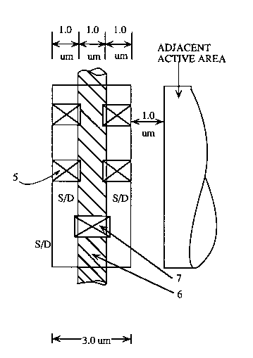
36 illustrated in Fig. 2. The self-aligning source/drain
37 contacts 5 can be made to overlap the gate 6. Thus, using
38 one micron layout rules, the transistor pitch in the
_ ABP/M-1004 2 0 3 4 0 7 5 PATENT APPLICATION
1 x-direction is 4 microns, approximately 30% smaller than the
2 prior art.
3 Referring again to Fig. 1, in the prior art, contacts,
4 such as contact 4, to the polysilicon gate are typically
5 allowed only in the field region, spaced 0.8 microns away
6 from the active region in order to avoid shorts to the
7 æource and drain regions due to worst case misalignment of
8 masks during the manufacturing process. AS illustrated in
9 Fig. 2, the self-aligning gate contacts 7 of this invention
10 can be made on top of the active region, saving considerable
11 space-
12 Referring to Fig. 3a, the method of forming a MOS field
13 effect transistor of a CMOS integrated circuit according to
14 this invention begins using well-known techniques to form N
15 and P wells 10, and field and gate oxidation areas 11 and 12
16 respectively on doped silicon substrate 13. Gate oxide 12
17 is typically 180 ~ thick.
18 Referring to Fig. 3b, a layer 14 of polysilicon about
19 3000 ~ thick is formed by low pressure chemical vapor
deposition (LPCVD) and doped typically by diffusion, with N-
21 type impurities to achieve a suitable sheet resistance,
22 typically 50 ohms per square. The doped polysilicon will
23 function as a gate in the complete MOSFET device. First
24 level interconnects, (not shown) usually located in the
periphery of a memory array, can also be formed from
26 this layer of polysilicon. Next a thin, 150A
27 oxide layer 15 is thermally grown on the polysilicon. A
28 layer 16 of silicon nitride about 1800 ~ thick is next
29 formed on oxide layer 15 by LPCVD.
Referring to Fig. 3c, the polysilicon gates 14a, 14b
31 are defined by well-known photo-masking and sandwich etching
32 techniques. The sandwich etch is carried out in a LAM
33 490. The anisotropic sandwich etch includes a SF6 plasma
34 etch of the silicon nitride layer 16 and silicon oxide layer
15 and a subsequent anisotropic C12/He plasma etch of the
36 polysilicon to form polysilicon qates 14a and 14b covered by
37 layers 15a, 15b and 16a, 16b.
38 Well known ion implantation techniques are next used to
~,~
.,'~
2034075
ABP/M-1004 PATENT APPLICATION
1 form botn N- and P- type lightly doped drain (LDD) implants
2 17a, 17b, 17c, 17d ~Fig. 3d) so that the LDD implants have a
3 conductivity type that is opposite to that of the well 10 or
4 the substrate 13 if no well is present. Typically, the
5 impurity concentration of the LDD implants is about 1.8 x
6 1ol3 dopant atoms per cubic centimeter. Chemical vapor
7 deposition of a silicon oxide layer using TEOS
8 (tetraethylorthosilicate (ethyl silicate)) at approximately
9 350-400 C followed by reactive ion etching forms gate
10 sidewall spacers 18a, 18b, 18c, 18d of silicon dioxide which
11 are approximately 4000-4200A thick. A layer of oxide 100 ~
12 thick (not shown) is thermally grown at approximately 800C
13 to cap the source and drain regions and to densify the
14 spacer oxide 18a-18d. N+ and P+ type source and drain
15 regions l9a, l9b, l9c, l9d are then formed by well known
16 masked ion implantation so that the dopant concentration is
17 typically 3 x 10¹⁵ - 5 x 10¹⁵ dopant atoms per cubic
18 centimeter in these regions.
19 Gate contact regions are defined as described below.
Referring to Fig. 3e, chemical vapor deposition of a silicon
21 oxide layer 20, 1100 ~ thick, is followed by annealing of
22 the layer at 875C for 30 minutes in a nitrogen
23 atmosphere-
24 The wafer is then coated with a standard Novolak based
positive photoresist available from Shipley which tends to
26 planarize the wafer, and is then baked. The photoresist 21
27 is blanket etched by oxygen plasma in plasma etcher AME 8115
28 until the oxide 20 covering the gate region i8 visible. A
29 second bake of resist layer 21 at 150 C for approximately
30 minutes hardens the resist 21 and makes it unreactive in
31 subsequent steps. A second layer of the same positive
32 photoresist 22, to be used with a dark field mask, is
33 applied over the first layer 21.
34 Next an opening is formed through oxide 20, nitride 16b
and oxide 15b to allow electrical contact to be made to gate
36 14b. The polysilicon isolation mask used for this purpose
37 to expose the gate 14b can have a contact size extending
38 beyond the gate, thereby permitting a looser alignment
2034075
_ ABP/M-1004 PATENT APPLICATION
1 tolerance. An approximation of the variable position of the
2 contact opening to gate 14a due to alignment tolerances for
3 the mask is shown by the dashed lines in Fig. 3f. The
4 presence of the first photoresist layer 21 prevents exposure
5 of the source and drain regions l9c,d during etching of the
6 oxide layers 20 and 15b and silicon nitride layer 15 to
7 expose the gate 14b, even in the event of worst case
8 alignment of the mask. In this way electrical contact to
9 the gate 14b can be made over the active channel region of
10 the transistor under gate 14b without causing a short
11 circuit between the source or drain l9c,d and the gate 14a.
12 A multi-step etch is conducted to expose the gate
13 contact. First, the oxide 20 is removed in the area exposed
14 by the opening 22a in resist layer 22 with a dry plasma etch
15 using C2F6/CHF3 in a 25:12 ratio. Secondly, 1200-1500 ~ of
16 the silicon nitride layer 16b is removed by a CF4 plasma
17 etch. However, CF4 etches all exposed materials at
18 approximately the same rate to help create a smooth profile
19 above gate 14b and causes a step in the oxide 18c, 18d at
the interface of the oxide 18c, 18d and the first layer 21
21 Of photoresist. Next, complete removal of both photoresist
22 layers 21, 22 is followed by a standard wet phosphoric acid
23 etch with a 50 to 1 selectivity toward silicon oxide (i.e.,
24 phosphoric acid etches silicon nitride fifty times more
rapidly than silicon oxide) which removes the remainder of
26 nitride layer 16b. Finally, a blanket CF4 plasma etch
27 removes 150 ~ thick oxide layer 15b and decreases the height
28 of the oxide step in oxide 18c, 18d on the sides of gate 14b
29 to produce the polysilicon gate contact 14c shown in
Fig. 3g. A process using only dry etchants for exposing the
31 gate contact is also feasible.
32 Referring to Fig. 3h, contacts to the source and drain
33 regions are defined using a buried contact mask. A 1:1
34 C2F6/CHF3 plasma etch of the oxide 20 removes only 10 to 20%
of spacer oxide 18a, 18b because spacer oxide 18a, 18b is
36 significantly thicker than oxide 20. The silicon nitride
37 layer 16a protects the gate 14a after some portion of the
38 oxide 20 covering the gate is removed. With spacer
-- 8 --
,.., I
203~
_ ABP/M-1004 PATENT APPLICATION
1 oxide 18a, 18b and protective silicon nitride layer 16a
2 intact on gate 14a, source and drain contact metallization
3 deposited later can overlap the gate without causing a short
4 circuit between the source and drain l9b and the gate 14a.
The plasma oxide etch is followed by a backside etch
6 which exposes pure silicon on the back side of the substrate
7 10. This exposure allows the temperature of the substrate
8 10 to be more closely monitored and controlled in subsequent
9 processing steps. The backside etch is conducted in three
10 steps. the first step using a 12:8 ratio of CHF3/SF6 in
11 helium is followed by a second step using only SF6 in
12 helium. The third step uses 20:8 CHF3/SF6, also in helium.
13 Referring to Fig. 3i, the silicon exposed by the
14 source, drain and polysilicon gate contacts and the
15 interconnects (not shown) are silicided by depositing a
16 layer of sputtered titanium about 700 ~ thick and using
17 rapid thermal annealing at 700C in a N2 atmosphere to form
18 a layer of TiSi coated by a thin layer of titanium
19 nitride. The rapid thermal annealing process involves
20 quickly heating the substrate to a predetermined
21 temperature, holding the substrate at that temperature for
22 30 seconds and then returning it to its original
23 temperature. The substrate can reach the predetermined
24 temperature as quickly as 15 seconds. The rapid thermal
annealing apparatus typically used is available from PEAK
26 SYSTEMS, model ALP-5500. The unreacted titanium is stripped
27 from the substrate's surface with a 5:1:1 solution of water,
28 hydrogen peroxide and ammonium hydroxide which also attacks
29 and removes the titanium nitride layer. A second rapid
thermal annealing step at 900C for 30 seconds in an
31 atmosphere of ammonia converts the TiSi to the stable
32 silicide TiSi2 layer 23a, 23b, coated by a thin layer of
33 titanium nitride (not shown). In this way, areas of
34 titanium silicide are selectively formed. For instance, the
3~ gate is silicided only at regions which will contact the
36 subsequently formed local interconnects because these are
37 the only gate regions exposed by previous processing steps.
38 Of importance, the silicided layer 23a, 23b can protect
_ g _
203~075
ABP/M-1004 PATENT APPLICATION
_ ,.
1 the underlying source, drain and gate regions and the
2 interconnects during later processing steps, particularly
3 the formation of local interconnects to be formed from a
4 second polysilicon layer.
Local interconnects are formed from a second layer of
6 polysilicon about 700 ~ thick which is deposited by LPCVD in
7 a well-known manner. However, before the wafers are
8 inserted into the reactor, the reactor temperature is
9 lowered to 150C. The reactor chamber is evacuated and
10 backfilled with an inert gas before the temperature is
11 raised so as to lessen the wafers' contact with oxygen at
12 high temperatures. Well-known masking and etching processes
13 define the local interconnects. Use of an isotropic SF6/02
14 plasma etch diminishes the necessity of overetch. Because
15 the etch is selective to titanium silicide, the underlying
16 titanium silicide layer 23a, 23b prevents damage to the
17 source, drain and gate contacts and the first layer
18 interconnects formed from the first polysilicon layer during
19 the etch, therefore, the local interconnects are not
required to completely overlap these regions. Layer 23 also
21 acts as an etch stop so that the etchant will not remove the
22 polysilicon gate or first layer interconnects during
23 overetching of the local interconnects.
24 Next, a 500A layer of sputtered titanium is deposited on
the substrate. Rapid thermal annealing at 640C in a
26 nitrogen atmosphere for 60 seconds forms titanium silicide
27 TiSix local interconnects 27 encapsulated by a thin titanium
28 nitride film. The unreacted titanium and the titanium
29 nitride film are stripped from the surface with a solution
of 5:1:1 water, hydrogen peroxide and ammonium hydroxide to
31 give the structure shown in Fig. 3i.
32 Referring to Fig. 3j, a 500 ~ thick layer of oxide is
33 deposited from a mixture of silane, nitrous oxide and
34 nitrogen at approximately 400C to act as an isolation
layer 29. Masking and a standard CHF3/02 plasma oxide etch
36 are used to open load resistor vias 30 to selected regions
37 of local interconnects 27. Rapid thermal annealing at 850C
38 for 30 seconds in a nitrogen atmosphere converts the TiSiX
-- 10
2034075
ABP/M-1004 PATENT APPLICATION
1 of the local interconnects to TiSi2 to create low resistance
2 interconnects. A thin titanium nitride film 28 forms on the
3 regions of the local interconnects exposed by vias 30.
4 Titanium nitride is a good electrical conductor but a
5 barrier to dopant diffusion. This barrier will prevent
6 dopants from diffusing into the polysilicon resistors formed
7 by subsequent processing steps.
8 A third layer of polysilicon 700 ~ thick, which will
9 constitute the resistors, is deposited in a well-known
10 manner by LPCVD. Masking and etching again using an
11 isotropic SF6/O2 plasma etch define resistors 31 as shown in
12 Fig. 3j. Dopant implantation to reduce the resistance of
13 the resistors is possible.
14 Referring to Fig. 3k, a layer 32 of oxide 1200-1500~
15 thick is deposited from a mixture of silane, nitrous oxide
16 and nitrogen at approximately 400C. A doped boron-
17 phosphorous glass 33 which acts as an insulation layer is
18 deposited over oxide 32 in a manner similar to oxide 32 but
19 with the addition of diborane and phosphine to the starting
gases. The glass 33 is flowed at 800C for 30 minutes to
21 form a more level surface. Oxide layer 32 prevents
22 diffusion of boron and phosphorus from boron-phosphorus
23 glass 33 to resistors 31.
24 Standard fabrication techniques are used to complete
the product.
26 Figs. 4a and 4b show the layout of a four cell CMOS 100
27 SRAM memory using this invention. A key illustrating which
28 materials are symbolized by which shading types is also
29 provided as Fig. 4c. Referring to Fig. 4a, which shows only
some of the cell components for clarity, each cell occupies
31 one quadrant as divided along lines A-A and s-B. The cell
32 dimensions, only 6 x 9 microns, illustrate of the small cell
33 size achievable according to this invention. Reference
34 numbers 40 and 42 indicate the field oxide and the island or
active area, respectively. The two conductive gates 44 per
36 cell are formed from the first deposited layer of
37 polysilicon. Contacts 46 to the polysilicon gates 44 can be
38 wider than the gates 44 themselves as indicated by the hash
ABP/M-1004 2 0 3 4 0 7 5 rATENT APPLICATION
1 lines 46a. Buried contacts 48 open to the source and drain
2 regions can overlap but not electrically and ohmically
3 contact gate 44 by the process described above. To form the
4 crosscoupled memory cell the circuit for which is shown as
S Figure 2 in the above referenced Canadian Application 2,034,057,
6 each buried contact 48 is connected to a gate contact 46 via a
7 conductive titanium silicide local`interconnect structure
8 50. Other components of each cell include the bit line
9 contact 52, the polysilicon word line 54, the silicided Vcc
10 56 and the silicided ground line 58.
11 Additional cell components are illustrated in Fig. 4b.
12 Load resistor vias 60 are located above a buried contact 48
13 and overlap a gate contact 46 as indicated by the hash
14 lines 60a. The location of the load resistors 62 is
indicated by a heavy line. A via 64 to the Vcc line 56 is
16 opened between two cells. Vertical heavy lines 66 and
17 horizontal stripes of shading 68 show the location of
18 connective metal lines formed by standard techniques.
19 Referring to Fig. 4c, shading 70 indicates titanium
silicide layers. Shading 71 indicates an island region.
21 Shading 72 shows cell components formed of polysilicon by
22 the first deposition of polysilicon. Hash lines 73 outline
23 the borders of the polyisolation mask which opensthe gate
24 contact. Shading 74 indi~ates bit contacts. Hash lines 75
outline load resistor vias. Heavy lines 76 outline load
26 resistors. Shading 77 indicates a contact region. Light
27 l-ines 78 show metallic interconnects. Field oxide in
28 Figs. 4a and 4b is not shown with shading or outlines but
29 occupies the white unmarked portions of the cell layout.
31
32
33
34
36
37
38
- 12 -