Note : Les descriptions sont présentées dans la langue officielle dans laquelle elles ont été soumises.
03-LO-6278
PATENT
STALL PROTECTION CIRCUIT FOR AN
ELECTRONICALLY COMMUTATED MOTOR
Background of the Invention
The invention generally relates to stall protection
circuits for motors and, in particular, a stall protection
circuit for an electronically commutated motor wherein the
circuit is part of the drive control for the electronically
commutated motor.
Some electronically commutated applications experi
ence excessive temperature rise at even normal operating cur
rent levels after operation under stall conditions. This is
due to the inability of the motor to dissipate heat built up
during the stall condition. In a stall condition, the lack
of air circulation inhibits heat dissipation. Hermetically
sealed motors are particularly sensitive to temperature rises
at or after stall conditions. Some hermetically sealed motors
under normal operation take full advantage of the cooling
capability of refrigerants being pumped through a system with
which the motor is associated. These motors are particularly
sensitive to temperature rise at stall when refrigerants are
not being pumped and the cooling capability has been lost.
The requirement for stall protection has typically
been met by monitoring the temperature and current of the
motor. In particular, temperature sensors are physically
attached to the stator windings and/or current sensitive sen-
sors are placed electrically in series with the windings. In
certain electronically commutated motor applications, the use
of such sensors is complicated by two factors. First of all,
as the electronically commutated motor drive provides a three-
phase current source to the motor, the current sensors have
to be three-phase protectors. Second of all, as the elec-
tronically commutated motor drive regulates the current, the
1
03-LO-6278
PATENT
iii~a.~~a~. ~1~
temperature sensors must operate solely on winding tempera-
ture rise, which slows their operation. In addition, this
slower operation causes a longer protection cycle requiring a
significantly longer test period to demonstrate the multi-
cycle capability of the device in a particular application.
In many electronically commutated motor systems the
motor drives a compressor drive and provides a speed refer-
ence signal to a system controller. In these systems, the
combination of the electronically commutated motor and the
system controller can be configured as a protection circuit
for stall conditions. However, the extra requirements placed
on the system controller can be very burdensome. It would be
desirable to provide a stall protection circuit which mini-
mizes the above disadvantages and provides responsive
protection to stalling.
Summary of the Invention
It is an object of this invention to provide a
stall protection circuit that permits a full torque be
delivered at the start of an interval of time adequate to
achieve some minimum operational speed of the motor under
normal conditions.
It is another object of this invention to provide a
stall protection circuit which, in the event of a stall condi-
tion, reduces the motor current below some maximum amount
before winding temperatures exceed the insulation breakdown
temperature ratings of the winding.
It is another object of this invention to provide a
stall protection circuit which is externally resettable after
it has functioned to protect the motor in a stall condition.
It is still another object of this invention to pro-
vide a stall protection circuit which fulfills a single mode
2
03-LO-6278
PATENT
~0:~~3~9
failure safe criterion to the maximum degree to readily
facilitate qualification.
It is an object of this invention to provide a cir-
cuit integral with an electronically commutated motor drive
control which can be qualified for safety, such as by
Underwriter Laboratories, as a stall protection circuit.
In one embodiment, the invention comprises a con-
trol circuit for a system including an electronically
commutated motor. The motor has a stationary assembly with a
plurality of winding stages for carrying a motor current in
response to application of a voltage. The motor also has a
rotatable assembly associated with the stationary assembly in
selective magnetic coupling relation therewith for rotation
at a motor speed in response to a magnetic field generated by
the winding stages. A commutating circuit for the motor is
responsive to a control signal for applying the voltage to
one or more of the winding stages at a time to commutate the
winding stages in a preselected sequence to rotate the rotat-
able assembly. Tachometer pulse signal generating means
generates a signal representative of rotation of the rotat-
able assembly. The control circuit comprises first and sec-
ond means. The first means inhibits application of the motor
voltage to the winding stages in response to the tachometer
pulse signal when the motor speed is below a preset minimum
speed thereby preventing the application of the motor voltage
when the motor speed is below the preset minimum speed. The
second means inhibits application of the motor voltage to the
winding stages in response to the tachometer pulse signal
when the duty cycle of the tachometer pulse signal is outside
a preselected acceptable range thereby preventing application
of the motor voltage when the duty cycle of the tachometer
pulse signal is outside the preselected acceptable range.
Application of the motor voltage to the winding stages is
3
03-LO-6278
PATENT
~U;~~~~~
inhibited when the motor is stalled as indicated by the motor
speed being below the preset minimum speed or as indicated by
the duty cycle of the tachometer pulse signal being outside
the preselected acceptable range.
S Other objects and features will be in part apparent
and in part pointed out hereinafter.
Brief Description of the Drawings
Figure 1 is a block diagram of one preferred embodi-
ment of a stall protection circuit according to the invention
in combination with an integrated circuit, power switching
circuit and motor.
Figure 2 is a schematic diagram of one preferred
embodiment of the stall protection circuit illustrated in
Figure 1.
Figure 3 is a timing diagram, relating to the ac
coupled motor voltage inhibiting circuit, illustrating the
waveforms of the tachometer pulse signal, the charge on the
ac coupling capacitor C03, the signal at the base of the con-
trol transistor of the 1/time circuit, the charge on capaci-
for COS applied to the collector of the control transistor,
and the charge developed on the motor speed signal capacitor
COS and applied to pin 9 of comparator U08.
Figure 4 is a waveform diagram, relating to the do
coupled circuit, illustrating the waveforms of the charge on
the duty cycle capacitor C60 applied to pin 4 of comparator
U07, the charge on the minimum duty cycle capacitor C61
applied to pin 5 of comparator U07 and the output level of
pin 2 of comparator U07 when the on/off signal is switched
high and the rotor is stalled at start.
Figure 5 is a waveform diagram, relating to the do
coupled circuit, illustrating the waveforms of the charge on
4
03-LO-6278
PATENT
~0~,3~~89
the duty cycle capacitor C60 applied to pin 4 of comparator
U07, the charge on the minimum duty cycle capacitor C61
applied to pin 5 of comparator U07 and the output level on
pin 2 of comparator U07 when the on/off level is switched
high, and normal operation occurs.
Figure 6 is a waveform diagram, relating to the do
coupled circuit, illustrating the waveforms of the charge on
the duty cycle capacitor C60 applied to pin 4 of comparator
U07, the charge on the minimum duty cycle capacitor C61
applied to pin 5 of comparator U07 and the output level on
pin 2 of comparator U07 when the rotor stalls during opera-
tion after normal starting and running.
Figure 7 is a waveform diagram relating to the ac
coupled circuit, illustrating the waveforms of the charge on
the minimum motor speed capacitor C57 applied to pin 8 of com
parator U08, and the output level on pin 14 of comparator U08
when the on/off signal is switched high and the rotor is
locked at start.
Figure 8 is a waveform diagram, relating to the ac
coupled circuit, illustrating the waveforms of the charge on
the minimum motor speed capacitor C57 applied to pin 8 of com-
parator U08, the charge on the motor speed signal capacitor
C08 applied to pin 9 of comparator U08 and the output level
on pin 14 of comparator U08 when the on/off signal is
switched high, and normal operation occurs.
Figure 9 is a waveform diagram, relating to the ac
coupled circuit, illustrating the waveforms of the charge on
the minimum motor speed capacitor C57 applied to pin 8 of com-
garator U08, the charge on the motor speed signal capacitor
C08 applied to pin 9 of comparator U08 and the output level
on pin 14 of comparator U08 when the rotor stalls after
normal starting and running.
5
03-LO-6278
PATENT
~;a:~~:389
Corresponding reference characters indicate
corresponding parts throughout the several views of the
drawings.
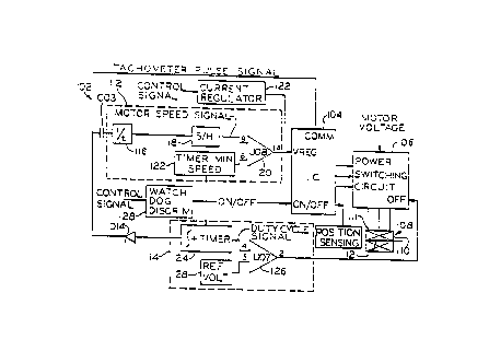
Referring to Figure 1, a control circuit generally
referred to by reference character 102 is responsive to a con-
trol signal provided by a system controller (not shown).
Circuit 102 provides signals to integrated circuit (IC) 104
for controlling a power switching circuit 106 to drive a
motor 108. Coassigned U.S. patent No. 4,500,821 invented by
Bitting et al., entitled Speed or Torque Control Circuit for
an Electronically Commutated Motor and Method of Controlling
the Torque or Speed of an Electronically Commutated Motor, is
incorporated herein by reference as an example of IC 104 and
power switching circuit 106 as is well known in the prior
art. In general, the purpose of control circuit 102 is to
receive the control signal from the system controller and con-
vert it into a signal which can be provided to control IC
104. The above-noted patent illustrates one example of such
a control circuit. As another example, motor 108 may be used
to drive a refrigeration compressor (not shown) in which the
refrigeration system controller generates the control signal
depending on the particular cycle in which the refrigeration
system is operating.
Motor 108 is an electronically commutated motor hav-
ing a stationary assembly 110 with a plurality of winding
stages 111 for carrying motor current in response to applica-
tion of a motor voltage supplied via the power'switching cir-
cuit 106. Motor 108 includes a rotatable assembly 112 mag-
netically associated with the stationary assembly in selec-
tive magnetic coupling relation therewith for rotation at a
6
03-LO-6278
PATENT
iC~~.~~a~. 8~
motor speed in response to a magnetic field generated by the
winding stages. Control circuit 102 is for use with a commu-
tating circuit for motor 108 such as IC 104 and is responsive
to the control signal for applying the motor voltage to one
or more of the winding stages at a time to commutate the wind-
ing stages in a preselected sequence to rotate the rotatable
assembly 112. The control circuit 102 is responsive to a
tachometer pulse signal generator such as IC 104 generating a
signal representative of the rotational speed of the rotat-
able assembly 110. For example, the tachometer pulse signal
may be a signal generated in response to position sensing
such as back emf sensing performed by IC 104.
Reference character 112 refers to a first motor
voltage inhibiting circuit for inhibiting application of the
motor voltage to the winding stages in the event that the
motor speed is below a preset minimum motor speed range, i.e.
an unacceptable motor speed indicative of a motor stall.
Reference character 114 refers to a second motor voltage
inhibiting circuit for inhibiting application of the motor
voltage to the winding stages in the event that a duty cycle
of the tachometer pulse signal, i.e., the active portion of
the tachometer pulse signal, is outside a preselected duty
cycle range, i.e. an unacceptable duty cycle indicative of a
motor stall. Preferably, the first motor voltage inhibiting
circuit is ac coupled to the tachometer pulse signal via a
capacitor C03 and the second motor voltage inhibiting circuit
112 is do coupled to the tachometer pulse signal, such as by
a diode 41. Therefore, the control circuit 102 according to
the invention includes two separate circuits which can be
used separately or in combination. The difference between
these circuits is the mode in which they are coupled to the
tachometer pulse signal and, as will be described below, the
type of monitoring of the tachometer of the pulse signal that
7
03-LO-6278
PATENT
~U:.~~;~~3~
the circuits perform. In general, the first inhibiting cir-
cuit 112 uses a capacitor coupled (ac coupled) tachometer
monitoring circuit which assures a safe shut down in the
event of a continuous high failure mode in the tachometer
pulse signal generated by IC 104. The second inhibiting cir-
cuit 114 is a direct coupled (dc coupled) tachometer pulse
signal monitoring circuit which assures safe operation in the
event of a fast running start oscillator used by IC 104 to
generate the tachometer pulse signal.
The first inhibiting circuit 112 includes an
inverse time circuit (1/t)~ 116 for generating a signal from
the ac coupled tachometer pulse signal which represents the
time (t) between pulses of the tachometer pulse signal. This
signal is provided to a sample and hold (S/H) circuit 118 to
generate a signal motor speed corresponding to the motor
speed. This motor speed signal is applied to the noninvert-
ing input pin 9 of a comparator 120. The inverting input pin
8 of comparator 120 is supplied with a reference voltage
which, except during start up as will be described below,
represents the minimum acceptable motor speed. As long as
the voltage on pin 9 representing the motor speed signal is
greater than or equal to the voltage on pin 8 representing
the minimum motor speed, the output pin 14 of comparator 120
remains high. This permits current regulator to process the
control signal and supply a current regulation signal input
to the VREG input of IC 120 which is responsive to the con-
trol signal. In the event that the voltage of the motor
speed signal on pin 9 falls below the minimum motor speed
voltage on pin 8, thereby indicating that the motor speed has
dropped below the acceptable level, the output of comparator
120 goes low to ground the VREG input of IC 104 and inhibit
the control regulation signal to prevent application of the
motor voltage to the winding stages.
8
03-LO-6278
The second motor voltage inhibiting circuit 114
includes an integrator and timer 124 which is do coupled to the
tachometer pulse signal and generates a duty cycle signal
corresponding to the duty of the tachometer pulse signal. In
general, the integrator and timer 124 integrate the tachometer
pulse signal over the period of time between pulses in order to
generate a signal representative of the duty cycle of the
tachometer pulse signal. As the active state of the commutate
pulse is low, reduced duty cycle operation which would accompany
m low speed results in an increase in voltage. This duty cycle
signal is provided to inverting input pin 4 of comparator 126.
Noninverting input pin 5 of comparator 126 is provided with a
reference voltage 128 representing the minimum acceptable duty
cycle. As long as the duty cycle signal on pin 4 indicates that
05 the duty cycle of the motor 108 is within a preset range, i.e.,
above the duty cycle represented by the reference voltage 128 on
pin 5, power switching circuit 106 is operational to provide a
motor voltage for application to the winding stages of motor 108.
In the event that the voltage of the duty cycle signal exceeds the
2o reference voltage 128, thereby indicating that the duty cycle is
below the minimum acceptable duty cycle, output pin 2 of
comparator 126 goes low to turn off the power switching circuit
106 and discontinue application of the motor voltage to motor 108.
In summary, the first motor voltage inhibiting circuit 112 assures
2~ a safe shutdown in the event of a continuous failure at the level
corresponding to the active state in the commutate signal derived
from the IC 104. On the other hand, the second motor voltage
inhibiting circuit 114 assures shut down in the event of a fast
running start oscillator in the control IC 104.
3o In addition, control circuit 102 may include a watchdog
discriminator 127 for recognizing the control signal and
0
~ Q ~ 4 3 ~ 9 03-LO-6278
activating the minimum speed generator 122 and the integrator and
timer 124. If the watchdog discriminator 127 is unable to detect
a control signal, both the minimum speed signal generator 122 and
the integrator and timer 124 are not activated and IC 104 is
turned off via its on/off input to inhibit operation of motor 108.
Referring to FIGS. 2 and 3, the components and
operation of inhibiting circuits 112 and 114 will be described in
greater detail. Capacitor C03 provides the referenced ac coupling
of the tachometer pulse signal to the first inhibiting circuit
l0 112. At each falling edge 302 of the tachometer pulse signal,
capacitor C05 is charged by transistor Q02. Thereafter, it
discharges through resistor R12 until the next falling edge 304.
During this discharging interval 306 between falling edges,
capacitor C08 has been charging through resistor R15. However,
15 the time constant of resistor R15/capacitor C08, i.e., R15 times
C08 is ten times the time constant of resistor R12 and capacitor
C05, i.e., R12 times C05. Furthermore, the resistance of R12 is
one-tenth of resistor R15. Ultimately, the charge on capacitor
C08 is determined by the final value to which capacitor C05
2o charges just before it is discharged by the next falling edge.
The voltage across capacitor C05 decreases as speed (the commutate
frequency) increases. The combination of these actions is that
the exponential charging of capacitor C05 approximates a 1/time
function, and the clamping of the voltage on capacitor C08
25 approximates a sample and hold circuit therefor. This produces a
tachometer monitoring circuit with a relatively rapid response
time and significant ripple voltage. Resistor R58 and capacitor
C59 may be added to minimize the ripple voltage.
The minimum speed generator 122 initially functions as
3o a timer. Before the control signal is provided, a timer
03-LO-6278
PATENT
~G~~~a~~'
capacitor C57 has been previously charged through a resistor
40 to full logic supply voltage V+. This assures more con-
sistent timing by the low leakage electrolytic capacitor C57
at start. When the on/off input goes high indicating that
the watch dog discriminator 128 has detected a control
signal, capacitor C57 begins discharging through resistors
R41 and R45. As a result, the voltage that is applied to in-
verting input pin 8 of comparator 120 begins to increase.
The action of the comparator 120 is to shut off the delivery
of current to the motor 108 should the voltage at the invert-
ing input pin 8 from the timer and minimum speed control 122
exceed the voltage f rom the sample and hold circuit 118 on
the noninverting input pin 9. Therefore, resistor divider
network of R40, R41 and R45 combine to set a minimum speed of
operation. The resistor R41 represents the maximum source
resistance to capacitor C57 while scaling the required volt-
age to the comparator 120 and minimizing the individual re-
sistance values in the network. Capacitor C58 filters noise
that would otherwise appear at pin 8 of the comparator 120.
The bias above zero on capacitor C59 combines with
the motor starting circuit of IC 104 to force an apparent
minimum speed, such as 85 rpm, on the tachometer pulse signal.
As a result, the control circuit 102 provides sufficient ini-
tial allowance for low speed operation during the start se-
quence of motor 108. After the capacitor C57 reaches its
final charged value, the speed of the motor 108 must be main-
tained above the minimum speed of operation for current to
the motor 108 to be maintained and to prevent an off signal
being provided to the power switching circuit 106.
Preferably, IC 104 provides a tachometer gulse
signal at its COMM (commutate) output that includes a start
function which forces commutation at a preset minimum fre-
quency to drive the rotor out of a zero torque alignment with
11
03-LO-6278
PATENT
the stator poles at the initialization of operation. This
start function can lead to a possible failure that would be
derived from a very high frequency tachometer pulse rate.
Such a failure would not cause the ac coupled first inhibit
ing circuit 112 to inhibit motor operation. For example, sup-
pose that a resistor/capacitor reference for the IC 104 start
function is reduced by component failure to the point that
the start oscillator within IC 104 produces a commutate fre-
quency great enough to exceed the minimum threshold for speed
in the ac coupled stall protection circuit. In such an
event, current to the motor would be maintained even if the
rotor were stalled.
In contrast, the do coupled circuit 114 does not
resgond in the same manner as the ac coupled circuit 112.
The do coupled inhibiting circuit 114 uses the fixed width of
the tachometer pulse supplied by the CO1~ output of IC 104 to
develop a duty cycle measuring circuit. The fixed pulse
width results in a measurement that is linearly proportional
to the frequency of the pulses. Resistors R35 and R39 along
with capacitor C60 constitute the integrator and timer 124.
This generates the duty cycle signal provided to the invert-
ing input pin 4 of comparator 126. Essentially, the rate at
which capacitor C60 is discharged by the high on/off signal
produces the timer function. The action of diode 41 coupled
to the inverted fixed pulse width tachometer pulse signal and
the averaging circuit of resistor R39 and C60 produce the
integration function. As in the ac coupled stall protection
circuit, the timer capacitor C60 is charged to full logic
supply voltage at the initiation of the start sequence.
Alternatively, in both the ac coupled and do coupled cir-
cuits, the timer capacitor C57 and C60 could be connected to
logic common and begin the timing function from a discharge
state without departing from the basic concepts according to
the invention.
12
03-LO-6278
When the watchdog discriminator 127 detects a control
signal, the on/off signal it provides goes high indicating an "on"
condition. As a result, the voltage that is supplied to the
inverting input pin 4 of comparator 126 begins to increase as the
voltage at capacitor C60 increases. However, the tachometer
pulses at diode 41 modulate the voltage supplied to the averaging
circuit of resistor R39 and capacitor 60 so that the final voltage
developed at capacitor C60 is limited by the tachometer pulse duty
cycle. As the pulse width is held constant for normal operation,
to the voltage at capacitor C60 is limited by the pulse signal
frequency. The higher the tachometer pulse signal frequency as
detected by diode D41, the lower the final voltage developed at
capacitor C60. The action of the comparator 126 is to shut off
the delivery of the current to the motor 108 should the voltage at
the inverting input pin 4 from the timer circuit 124 exceed the
voltage from the fixed reference voltage at the noninverting input
pin 5. The resistor divider network of resistors R68 and 8103
combine to define a voltage representative of a minimum speed of
operation after the start time out. The start time out is the
2o period during which capacitor C60 is charging from full logic V+
to its maximum as limited by the tachometer pulses. Capacitor C61
filters noise that would otherwise appear at the noninverting
input pin 5 of comparator 126.
As noted above, the ac coupled stall protection
2s circuit 112 would not inhibit motor operation if the resistor/
capacitor (R/C) reference for the start function for IC 104 is
reduced by component failure to the point that the start
oscillator in IC 104 produces a commutate frequency great enough
to exceed the minimum threshold for speed in the ac coupled
3o stall protection circuit 112. In contrast, the do coupled
circuit 114 would not respond in the same manner.
13
03-LO-6278
PATENT
~(~~343~9
The same R/C reference for the start oscillator sets the
pulse width for the commutate pulse. The commutate pulse
width is one period of the start oscillator and the start com-
mutate period is a preset number of oscillation periods,
i.e., 193 oscillator periods. The start function then pro-
duces the same output to the do coupled stall protection cir-
cuit 114 regardless of start oscillator speeds because of the
duty cycle measurement feature of the do coupled circuit.
It is also important to note that the ac coupled
circuit 112 and the do coupled circuit 114 insert their
respective current shutdown signals into different sites of
the motor control. In particular, the ac coupled circuit 112
inhibits the VREG input of IC 104 to inhibit application of
the motor voltage to motor 108 by shutting down commutation.
On the other hand, the do coupled stall protection circuit
112 actuates stall protection by providing an off indication
to the power switching circuit 106 to prevent the application
of the motor voltage to the winding stages of the motor 108.
This further enhances the single mode fail safe features of
the combined control circuit 102.
Figures 4-6 illustrate the operation of the do
coupled circuit 114. In Figure 4, line 40Z represents the
reference voltage being applied to the noninverting input pin
5 of comparator 126 (U07) as generated by the reference volt-
age source 128. Line 404 represents the low level at output
pin Z of comparator 126 (U07) through the action of other
control circuitry (not shown) before the control signal is
provided and before the watch dog discriminator 128 provides
a high signal indicating an "on" condition. When the on/off
signal is switched high by discriminator 128,Ithe voltage at
output pin 2 is allowed to go high as illustrated by line
406. If the rotor is locked at start, the voltage on invert-
ing input pin 4 as illustrated by line 408 steadily increases
14
03-LO-6278
PATENT
~03~~~0
as capacitor C60 charges from bias level 407 until it reaches
its maximum level 409. At point 410, when the voltage Ievel
408 on pin 4 exceeds the voltage level 402 on pin 5, pin 2
drops low level 412 to discontinue application of motor volt-
s age to the motor windings.
Circuits 112 and 114 have been described for use in
combination with a tachometer pulse signal having negative
commutation pulses. It will be apparent to those skilled in
the art that other, similarly designed circuitry may be
employed for positive commutation pulses. Alternatively,
other components may be employed to follow the tachometer
signal such as a comparator or operational amplifier.
Alternatively, other components may be used to provide
coupling such as a base-collector as a decoupler.
Figure 5 illustrates the waveforms of the do
coupled circuit 114 during normal operation. When the on/off
signal is switched high, the voltage at output pin 2 is
allowed to go from the low level 404 to the high level 406.
The voltage on pin 4, which is the voltage level of capacitor
C60, increases from bias level 407 to a steady state 502.
This steady state 502 is below level 402 because of the modu-
lation of the tachometer pulses. As long as the duty cycle
of the tachometer pulse signal as represented by line 402 is
above the preset minimum duty cycle as represented by line
502, output pin 2 remains high. This is because the voltage
level _502 being applied to inverting input pin 4 of compa-
rator 126 remains below the voltage level 402 of noninverting
pin 5.
Comparing Figures 4 and 5, it can be. appreciated
that do coupled circuit 114 inhibits application of the motor
voltage only after a preset period as illustrated in Figure
4. This period begins when the on/off signal is switched
high and ends at point 410 when the charge on capacitor C60,
o3-LO-sz78
PATENT
~w~~'4~.~. ~~
representing the duty cycle of the tachometer pulse signal,
equals or exceeds the reference voltage 128 representing the
maximum acceptable duty cycle. This preset period (or delay
in the activation of the inhibit function) permits the motor
to employ any type of start-up procedure, such as a soft
start as noted in coassigned U.S. patent 4,763,347,
incorporated herein by reference.
Figure 6 illustrates the waveforms of the do
coupled circuit 114 in the event that the rotor stalls during
normal operation. The lack of tachometer pulse signals per-
mits the voltage applied to pin 4 to begin to increase from
bias level 407 to the steady state level 502. At point 602,
it begins to increase again to a fully charged level 503 for
capacitor C60 and then maintains that level. At point 604,
when the increasing voltage level on pin 4, becomes greater
than the level of voltage on pin 5, the output of comparator
126 drops from the high level 406 to the low level 404.
Figures 7-9 illustrate operation of the ac coupled
circuit 112. Figure 7 illustrates operation when the rotor
ZO is locked at start. When the on/off signal is switched high,
the voltage being applied to inverting input pin 8 begins to
steadily increase from a bias level 702 to a steady state
level 704 as capacitor C57 discharges. Because the rotor is
locked, the bias voltage 706 being applied to noninverting
input pin 9 as determined by the charge vn capacitor C08 does
not substantially change (other than the ripple as illus-
trated in Figure 3). When the on/off signal is switched
high, output pin 14 is allowed to go from a low level 708 to
a high level 710 to permit current flow by action of the IC
and the current regulate circuit. However, at paint 712 the
voltage on pin 8 becomes equal to or greater than the voltage
on pin 9 so that pin 14 drops to low level 708 to inhibit any
further current delivery to the winding stages by action of
the IC.
16
03-LO-6278
PATENT
~U~43~9
Figure 8 illustrates the operation of the ac
coupled circuit 112 during normal conditions. When the
on/off signal is switched high, the voltage on pin 8 begins
to steadily increase from bias level 702 to steady state
level 704 as capacitor C57 discharges. When the on/off
signal is switched high, the voltage on capacitor C08 and
applied to pin 9 also moves from bias level 706 to a higher
level 802 because the tachometer pulses reduce the discharge
time of capacitor COS thereby increasing the charge on capaci-
for C08. As a result, the voltage level on pin 9 stays above
the voltage level on pin 8 so that output pin 14 goes from
low level 708 to high level 710 and remains high to permit
the action of the IC to commutate the winding stages.
Immediately after the on/off signal is switched high, the
voltage on pin 8 tends to vary between low level 708 and high
level 710 because the voltage on pin 8 is being controlled by
the current regulator 122 during this period. This is gener-
ally illustrated in Figure 8 by the area referred to by refer-
ence character 804.
Comparing Figures 7 and 8, it can be appreciated
that ac coupling circuit 112 inhibits application of the
motor voltage only after a preset period as illustrated in
Figure 7. This period begins when the on/off signal is
switched high and ends at point 712 when the charge on
capacitor C57, representing the minimum acceptable speed,
equals. or exceeds the charge on capacitor C08 representing
the motor speed. This preset period (or delay in the acti-
vation of the inhibit function) permits the motor to employ
any type of start-up procedure, such as a soft. start.
Figure 9 illustrates the operation of the ac
coupled circuit 112 when the rotor stalls after a period of
normal running. As in Figure 8, when the on/off signal is
switched high, both pins 8 and 9 increase in voltage. The
17
03-LO-6278
PATENT
~Ci~a.~~t~8~
voltage level on pin 9 goes from bias level 708 to steady
state level 802. The voltage level on pin 8 remains below
the level on pin 9 and goes from bias level 702 to steady
state level 704. When the rotor stalls, the voltage on
capacitor C08 and being applied to pin 9 immediately drops
from level 802 to level 708 because the lack of tachometer
pulses increases the discharge time of capacitor COS which,
in turn, reduces the charge on capacitor CO8. Level 708 is
below the level of pin 8 at point 902. As a result, the out-
put of pin 14 drops to low level 706 to inhibit application
of the motor voltage to the winding stages.
In view of the above, it will be seen that the
several objects of the invention are achieved and other
advantageous results attained.
As various changes could be made in the above
methods without departing from the scope of the invention, it
is intended that all matter contained in the above
description or shown in the accompanying drawings shall be
interpreted as illustrative and not in a limiting sense.
18