Note : Les descriptions sont présentées dans la langue officielle dans laquelle elles ont été soumises.
83~
LIDAR ~:CANNIN~ SY5~EN
Backqround and Summary of the Invention
This invention relates to a Light Distancing and
Ranging scanner (LIDAR) and particularly to a LIDAR scanner
employing a rotating polygon mirror for directing the scanned and
received light.
Three-dimensional imaging systems have improved the
performance of a wide variety of automation systems. While
three-dimensional images can be computed from multiple sets of
two-dimensional images, this approach is more complex and less
accurate than systems which collect images that are fundamentally
three-dimensional. In general, these systems collect large
amounts of three-dimensional coordinate data from visible
surfaces in a scene. This data consists of image data points
that explicitly represent scene surface geometry of each sampled
point by utilizing range information for each point.
One approach to three-dimensional vision is the l'time
of light'l approach which measures the range at given points by
measuring the timing of the return of a pulse of light projected
on a target. Unfortunately, the extreme electronic speed
required for this approach severely limits the resolution of such
systems. LIDAR sy~tems avoid the problems of the time of light
approach by modulating a light beam and comparing the modulation
of the transmitted and returned signal to determine range. For
instance, coherent frequency modulator tFM) LIDAR incorporates
frequency modulation/mixing to determine range. However, FM
LIDAR systems suffer from the limited frequency modulation
~3~3~
capabilities of current laser diodes. Phase shift (AM) LIDAR is
a preferred approach which correlates the phase shift between
outgoing and incoming amplitude modulated light beams to
determine range. As a result, each pixel in a collected image is
an individual range measurement, .and the resulting image is
somewhat like a "terrain map" of the scanned area. When the
range information is combined with the two-dimensional image,
true three-dimensional vision is accomplished.
A number of difficulties are encountered in the
opto-mechanical design of LIDAR systems. One is achieving an
acceptable signal-to-noise ratio. For example, LIDAR scanning
systems often utilize the same optical path for the transmitted
and received light. However, small particles of dirt or
scratches in the optical elements, or windows, can cause the
transmitted light to be received directly back into the receive
optics as noise or crosstalk.
Further, LIDAR systems frequently receive light from
the entire scanned volume simultaneously. In these systems the
field of view is the same as the scanned volume. This approach,
however, yields a relatively small signal-to-noise ratio for a
given output of light power. One alternative approach is to
receive the reflected radiation via a scanning system so that the
field of view of the receiving optical subsystem is very small.
This increases the signal-to-noise ratio to permit better
accuracy and to allow the use of a lower output light
transmitter. Further, in such systems since the transmitted
light beam is relatively narrow and the field of view of the
20~3~39~
receiver optics is narrow, it is easier to construct a system
where the outgoing and incoming light beams are not coaxial and
do not coincide. One approach, for example, uses dual rotating
polygon mirrors, one for transmitting the scanning output beam
and the other rotating polygon mirror being employed to receive
the incoming reflected light. However, the dual rotating polygon
approach presents alignment problems to ensure that the field of
view is coincident with the transmitted light.
Thus, it is desirable to provide an improved
three-dimensional imaging system which employs amplitude
modulated LIDAR with an improved signal-to-noise ratio. Further,
it is desirable to provide a LIDAR system in which the transmit
and receive beams are not coaxial to reduce unwanted reflections
and crosstalk. In addition, it is desirable to have a LIDAR
system which employs a small field of view that is scanned along
with the transmitted beam and which avoids the use of separate
polygons that must be accurately aligned.
~ LIDAR scanning system achieving the above-mentioned
desirable features is provided according to this invention. The
LIDAR scanning system includes a single rotating faceted polygon
mirror for receiving and reflecting a transmitted light beam
along a linear path as the polygon mirror rotates. Diffuse light
reflected from the scanned surface is received by the rotating
polygon mirror along an optical path at a small parallax angle
relative to the transmitted optical path. The received light is
reflected by the rotating polygon mirror and directed to a
sensor. The transmitted and returned beams are reflected by
;~389~
adjacent facets of the polygon mirror. In this way, the field of
view of the sensor is scanned and is coincident with the point on
the object receiving the scanned light.
In accordance with another embodiment of the present-
invention, the scanning system also employs a tilting mirror
which reflects both transmitted and received light for creating a
linear scan and receive pattern. The tilting mirror creates
scans along multiple positions of the Y-a~is to generate a
rectangular frame scan.
Additional benefits and advantages of the present
invention will become apparent to those skilled in the art to
which this invention relates, from the subsequent description of
the preferred embodiments and the appended claims, taken in
conjunction with the accompanying drawings.
Brief Descri~tion of the Drawinqs
Figure 1 is a diagram of the LIDAR scanner in
accordance with the invention showing the path of the scan beam
reflected from a scanned surface;
Figure 2 is a diagram of the outgoing and returning
amplitude modulated light signal indicating the phase shift due
to the distance of the light path;
Figure 3 is a diagram of the amplitude modulated light
signal indicating the tunable standoff, ambiguity interval, and
measurement range of the LIDAR scanner;
Figure 4 is a diagrammatic view of the opto-mechanical
portion of the LIDAR scanner shown in Figure 1, in accordance
with the invention;
Figure 5 is a diagram of the transmit telescope of the
LIDAR scanner shown in Figure 4; .~
Figure 6 is a diagram of the receive telescope of the
LIDAR scanner shown in Figure 4;
Figures 7~ - 7C are views of the field stop shown in
Figure 6 with images depicted at near, middle, and far ranges;
Yigure 8 is an overall block diagram of the LIDAR
system shown in Figure 1, including electronic circuits used to
control the scanner and to measure and process range information
scanning apparatus;
Figure 9 is a diagram illustrating a typical measuring
zone of the scanner according to the present invention;
Figure 10 is a LIDAR scanner in accordance wi~h a
second embodiment of the present invention for generating a
linear line scan pattern; and
Figure 11 is a block diagram of a robot bin picking
cell using the LIDAR scanner in accordance with the present
invention.
Detailed Description of the Invention
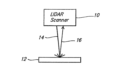
A LIDAR scanner 10 in accordance with the present
invention is shown in Figure 1. The I,IDAR scanner lO ohtains
image and range information from a surface 12 by transmitting a
beam of light 14 to the object surface 12 and detecting a diffuse
.
.
portion 16 of the transmitted light 14 which returns to the
scanner 10. While surface 12 is shown to be flat for sake of
simplicity, it will be appreciated that typically surfaces of
objects to be scanned will be optically rough and will produce
diffuse reflected light. In açcordance with the present
invention, a small parallax angle exists between the outgoing
beams 1~ and incoming beams 16. While this angle is exaggerated
in Figure 1 for illustration purposes, this angle will typically
be less than 0.5 degrees. This parallax angle reduces the
effects of light scatter and crosstalk by allowing the two beams
14, 16 to use different optical elements. In addition, it is
inmportant that the parallax angle remain relatively small to
minimize the "shadow effect" problems associated with larger
angular separation between the projection and detection axes.
This helps to ensure good acuity around steep surface 12
transitions.
Figure 2 shows how a phase shift measurement is
performed by comparing the relative offset of the positive~going
zero crossings of the outgoing and incoming modulated signals.
The outgoing modulated beam 14 is shown as an amplitude modulated
signal at relatively high power. The return signal 16 is also
modulated and is typically six orders of magnitude less in
amplitude than the outgoing signal 14. The phase shift 1~
between the outgoing signal 14 and returning signal 16 can be
correlated into an accurate range measurement by the use of
pre-established calibration data. That is, by knowing the
distance that the amplitude modulated wave travels during one
--6--
; 8 ~
cycle of modulation and the particular phase shift of the return
signal relative to the outgoing signal, the distance of the
ob~ect relative to a pre-established datum can be determined. It
should be noted that current circuitry cannot differentiate
between adjacent cycles of the ~ amplitude modulated wave.
Therefore, ranging can only be ac~omplished over one wavelength
of the modulated wave.
Referring now to Figure 3, the manner in which the
measurement range of the scanner 10 is established will now be
explained. Since the scanner 10 determines range by comparing
the relative phase shift of the incoming signal to the outgoing
signal, it will be appreciated that a surface 12 located one-half
of a wavelength of the modulated wave away from a zero crossing
point in the waveform (a distance designated 22 in Figure 3) will
result in a reflected signal exactly 360 degrees out of phase
with the transmittsd signal (i.e., one-half wavelength to reach
the surface and one-half wavelength to return). Accordingly,
since the scanner cannot detect a phase shift of 360 degrees, it
will be appreciated that an "ambiguity interval" 20 occurs once
each half cycle of the modulated waveform. Therefore, to prevent
an ambiguity interval from occurring within the measuring zone of
the scanner lO, the depth of the measuring zone must be limited
to less than one-half of a wavelength. In practice, the usa~le
measuring range 24 is limited to a distance corresponding to
slightly less than one-half of a wavel ngth due to the higher
noise content present in the reflected signal adjacent the
ambiguity intervals 20. Typically, 90 percent or more of the
half wavelength i5 useful for ranging.
Accordingly, to create a desired measuring range 24,
the transmitted light signal 14 must be modulated at an
appropriate frequency. For example,~ to create a measuring range
24 of 40 inches, a modulation frequency of 147.5 MH~ is required.
In addition, as will subsequently be described in greater detail,
the spatial positioning of the ambiguity intervals 20 can be
adjusted during calibration of the scanner 10 to define the
desired spatial position of the measuring range relative to the
scanner, referred to as the scanner "standoff". Preferably, the
point of focus of the light source transmitting telescope optics
is also set to be coincident with the center of the measuring
range 24.
Referring now to Figure 4, the opto-mechanical portion
26 of the LIDAR scanning system 10 in accordance with a preferred
embodiment of the present invention is shown. The source of the
scanning beam is a conventional laser diode 28 that is amplitude
modulated by modulation circuitry described below. For example,
laser diode 28 may be a phased array laser diode operating at 810
nanometers in the near infrared region. The amount of laser
power delivered to the target determines in part the system
signal-to-~oise ratio and therefore effects the quality of the
resulting image. For example, for a system with a two meter
standoff such as the bin picking application illustrated in
Figure 11, a laser 28 with an output of 200 milliwatts is
generally adequate. It will be appreciated, however, that losses
Z~)3~9Z~
in the optical path will reduce a 200-milliwatt beam to about 80
milliwatts of power at the target.
The output of the laser diode 28 is directed into a
transmit telescope 30 which collimates the laser output beam.
Figure 5 shows the transmit teles~.ope 30 in more detail. The
diverging beam from the laser diode 28 is shown at 32, first
entering a 30-millimeter collimator 34 and then passing through a
pair of brewster prisms 36 and a 3,533-millimeter focusing lens
38. The beam 32 is collimated just prior to focusing to avoid
placing the brewster prisms in a convergent beam since they would
then introduce astigmatism into the beam. The focusing lens 38
focuses the beam 32 onto the target to be scanned. It will be
appreciated that the far field pattern of a laser diode indicates
that the energy is divided between two lobes separated by a
finite distance with almost no energy in this separation. As a
result, the transmit optics capture only a portion of these two
lobes. It is preferable, therefore, to tilt the laser diode 28
so that the transmit telescope 30 entirely captures one lobe,
with a collection efficiency of about 92.5 percent for the single
lobe.
From the transmit telescope 30, the beam 32 is
reflected off a pair of folding mirrors 40, 42 which direct the
beam to one facet 45 of a rotating polygon mirror 44, as shown in
Figure 4. A motor and drive circuitry, described below, is
mounted to th~ reverse side of base 46 and causes the eight-sided
polygon mirror 44 to rotate at a desired angular rate. The
rotation of the polygon 44 transforms the laser beam 32 into a
~g _
circular arc that, when intersecting a planar surface, creates a
line scan for the lateral (x) image axis. For example, the
eight-sided mirror 44 rotating at 31.9 Hz (1,914 rpm) will
provide approximately 255 sweeps per second.
Thé transmitted beam 32 ls reflected off the rotating
mirror 44 onto a tilting mirror 48 which is mounted to a
galvanometer servo motor 50. The axis of the tilting mirror is
orthogonal to that of the polygon mirror 44. The tilting mirror
motion creates the longitudinal (y) image axis. The tilting
mirror, for example, may be rotated with a beam sweep rate of 8.9
degrees per second. Thus, it will be appreciated that the
rotating poly~on mirror produces a rapid X-axis scan of the laser
beam while the tilting mirror causes the X-axis line scan to
slowly sweep along the Y-axis.
The receive optics are focused to receive diffuse light
from the spot on the object 12 illuminated by the transmitted
beam 32 that is reflected off the tilting mirror 4~ onto the
adjacent facet of the polygon 44 and then reflected by the
folding mirror 56. It will be appreciated that the incoming beam
52 will generally be about six orders of magnitude below the
laser's output power (i.e., milliwatts transmitted become
nanowatts received).
As shown in more detail in Figure 6, the receive
telescope 5~ includes an objective lens 60 which may be, for
example, a 54-millimeter objective lens which is focused at 4
meters. A field stop 62 is located at the image plane of the
objective 60. The incoming beam 52 is then imaged onto a
--10--
X~ 2~
photodiode detector 64 by a relay lens ~6 which may ha~Je, for
example, a magnification o~ 0.6x. In addition, a narrow bandpass
optical filter (not shown) ma~v further be used to reduce
background radiation.
Referring now to Figures~7~ - 7C, the preferred field
stop 62 in accordance with one embodiment of the present
invention is shown. In Figure 7A, field stop 62 is shown as a
circular opaque disk with a triangular aperture 68 at its center.
The laser spot 70 is shown as it would appear at near range
located at the wide end of the aperture 68. As the distance to
the object 12 increases, the image formed by the spot 70 moves
toward the narrow portion of the aperture, due to the
triangulation effect of the parallax angle between the output and
input beams. Thus, Figure 7B shows the laser spot 70 at mid
range while Figure 7C shows the spot at far range in the narrow
portion of the aperture 68. In addition, it can be seen that as
the spot moves from near range in Figure 7A to far range in
Figure 7C, its size decreases due to the smaller magnification.
The field stop 62 thus, as shown in Figures 7A - 7C, is designed
so that the edges of the image of the laser spot 70 are nearly
tangent to the edges of the field stop aperture 68. The effect
is to block as much extraneous background radiation from reaching
the photo detector 64 as possible without reducing the strength
of the received signal. This has the effect of improving the
signal-to-noise ra~io.
Referring again to Figure 4, a zero reference system 72
is shown which is used to calibrate phase information of the
--11--
z~
received beam relati~e to the transmit beam 32. The zero
reference system 72 includes a pair of fiber optic light pipes 74
which each capture a small but consistent portion of the trailing
edge of the lateral (x) scan and feed it directly into the
receive telescope 5~. In particular~ the transmit beam 32 enters
the light pipes 74 at an input terminal aperture end 76 located
adjacent to the tilting mirror 48. The light pipes 74 comprise a
pair of ~0 micrometer multimode graded index optical fibers with
a numerical aperture of 0.2. The light passing through the
fibers 74 is collimated by a pair of aspheric lenses 78 with a
focal length of 3.2 millimeters. The collimated beams are then
introduced into the receive telescope 58 through mirrors 80 and
are focused onto the photodiode 6~ using the same optics as the
receive beam 52, but displaced off axis. These fibers 74 are
significantly different in length so as to provide two fixed and
known distance references for the LIDAR scanning system 10 to
eliminate circuit drift. In other words, received light from
each of these two fibers 74 exhibit a predetermined phase shift
relative to the transmitted light signal in accordance with the
preselected lengths of fiber optic cable used. In the preferred
embodiment, the length of one of the fiber optic cables is
selected to correspond to twice the distance to one extreme of
the scanner measuring range and the length of the other fiber
optic cable is selected to correspond to twice the distance to
the other extreme of the scanner measuring range. The zero
references are utilized by the electronics (described below) to
~)3~
calibrate the sys~em after each X-axis line scan (i.e., 255 times
each second).
In one embodiment of the present invention, the
opto-mechanical scanniny system 26 can provide an image frame
size of 1,024 x 1,02~ pixels, a pi~el rate of 360,000 pixels per
second, and a frame scan period of about 5 seconds. Also, a
range accuracy of about 0.040 inches can be achieved.
Referring now to Figure 8, the primary electronic
circuits o~ the LIDAR scanner system 10 are shown. The laser
diode 64 is shown mounted to a power driver and thermal control
module 82. The circuits within this module utilize the photo
detector, thermo-electric cooler, and thermistor that are
typically integrated into a laser diode package to rigidly
stabilize the laser's output power and case temperature. The
tightly controlled DC power of the laser is then deeply modulated
by an incoming signal 8~ from a UHF generator 86.
The photodiode which may be, for example, an avalanche
photodiode 64, is shown mounted to a voltage bias module 88.
Avalanche photodiodes provide very low noise and high dynamic
range for detecting the laser's diffuse return reflection. This
is important since the power recPived by the photodiode 6~ will
typically be six orders of magnitude below the laser's output
power. The UHF generator module 86 incorporates an ultra-stable
28 MHz crystal oscillator to frequency synthesize 90 N~Iz and 80
MHz signals. The 80 M~z signal is used to power modulate the
laser diode. The 90 MHz signal is mixed with both the laser
drive signal and the return signal detected by the avalanche
-13-
Z~3~
photodiode 64 in order to frequency shift the signal and the
reference channels down to 10 MHz where the analog phase
detection occurs. Appropriate bandpass filtering is provided in
this module 86 to remove the effects of ambient light and to-
minimize the proliferation of harmonics throughout the system
that might result in phase errors.
A phase detector module 90 executes analog phase
detection over a wide range of signal amplitudes and employs
circuitry that eliminates error due to even harmonic distortion.
The phase detector module 90 also provides a signal 92 that is
proportional to the intensity of the detected signal. This
intensity information signal 92 is utilized to refine range
measurements as a function of signal magnitude and can also be
used for gray scale imaging. The phase detector module 90 also
receives the zero reference calibration signals 96 that are
stripped off each data line by an A/D converter module 94. These
zero reference signals 96 eliminate long-term drift from the
system. In particular, the "measured" ranges of the two zero
reference calibration signals are determined following each
X-axis scan and compared with prestored values. Any variation
observed between the measured values and the prestored values is
then used to adjust the zero point and the slope of the voltage
versus ran~e line for the following X-axis scan.
The A/D converter module 94 provides tWQ parallel
channels of sample and hold A/D converters: 12 bits for phase
(range) information 98 and 11 bits for intensity data 100~ The
phase measurement information is combined with the intensity
~(~38~
information to provide an input address to a calibration table
(not shown) which has prestored therein range correction data.
As will subsequently be described in greater detail, the
intensity data is used to compensate for the differential phase
phenomenon inherent in the signal~processing of the received
signal to improve the accuracy of the system. The range and
intensity data 98, 100 are transmitted to a timing and
communication module 102 over parallel data lines 98, 100. Pixel
timing is required for synchronizing the A/D converters with the
system's rotating polygon mirror 44. In particular, the pixel
timing signal on line 104 triggers the A/~ converter module 94 to
digitize the detected phase difference ~etween the outgoing and
incoming signals 1,024 times for each X-axis sweep of the laser
beam.
The polygon mirror 44 is shown mounted to a hysteresis
synchronous motor 106. This drive motor receives its power from
a synchronous motor driver 108 which incorporates a low-jitter
crystal oscillator to generate the stable mirror velocity. An
incremental optical encoder 110 attached to the rear of the
polygon motor 106 generates a high frequency pi~el reference
pulse stream on line 112 that is provided to the tlming and
communication module 102 and serves as a reference for the
generation of the precise pixel timing pulses on line 104.
A start of scan detector 114 is provided which
comprises a highly collimated narrow aperture laser diode and
detector pair that creates a pulse at the center of each facet on
the polygon 114. This signal is used to synthesize a precise
-
32~
line synch signal on the start of scan data line 116 provided to
the timing and communication module 102. As will subsequently be
described in greater detail, the start of scan signal on line 116
is used by the timing and communication module 102 to identify
the start of the 1,024 pixel timin~.pulses on line 104 associated
with each X-axis sweep.
The tilting mirror 48 is shown mounted to a galvo servo
motor 50. The galvo servo motor 50 receives motion control
voltages 119 from a servo motor driver 118 and closes the servo
loop by feeding back a mirror position signal 120. The servo
driver 118 receives digital position signals along line 122 from
the digital position module 124 which derives the signals from
the mirror sequence commands 126 received from the timing and
communication module 102. In addition, the digital position
module 124 receives a start of frame pulse signal on line 128 to
synchronize the movement of the tilting mirror 48 with the rest
of the system.
The timing and communication module 102 is incorporated
to unify and synchronize the functions of all scanner 10
subsystems. It utilizes the pixel reference signal 112 to
synthesize the pixel clock signal for the system. At the pixel
rate, it receives the parallel range and intensity line signals
98, 100 and converts them to differential serial signals for
transmission to a scanner interface (not shown) along lines 130
and 132. Within the timing and communication module 102, the
bit, word, line, and frame si~nals 134, 136, 138, 140 are derived
and transmitted to allow the scanner interface to properly
-16-
89~
register and store the image data. The timing and communication
module 102 also receives the start of scan signal 116 and
utilizes this for both line framing and for triggering the start
of frame signal 128 for the tilting mirror 48. Finally, this
module 102 receives differential sçrial mirror sequence commands
148 and converts them to single-ended serial command signals for
use by the digital position module 12~.
In addition, it will be appreciated that the timing and
communication module 102 may also be used to implement a laser
power speed interlock so that the scanner 10 will only generate
at a constant "raster scan" mode. This may be accomplished, for
example, by requiring the polygon mirror 44 to be in motion for
the laser to operate. As a result, the scanner 10 can be
considered to operate as a pulsed laser device.
With additional reference to Figure 9, the manner in
which the scanner standoff is established will now be explained.
As previously noted, it is desirable to calibrate the scanner so
that an ambiguity interval does not occur within the desired
measuring zone. For e~ample, in a typical application with the
scanner 10 operating at a modulation frequency of 147.5 M~z, the
depth of the desired measuring zone 180 may be 40 inches and the
desired standoff distance 182 from the scanner 10 to the
measuring zone 180 may be 76 inches. To calibrate the scanner
for this type of application, it is necessary to locate an
ambiguity interval substantially coincident with the top 184 of
the measuring zone 180. This is readily accomplished in the
following manner. With additional reference to Figure 8, it will
-17-
:
g2~
be recalled that the photodiode ~ias module 88 supplies the
return signal received by the photodiode 64 to the phase
detection circuitry 86 and 90. The physical length of the
electrical cable ~5 used to carry this signal, therefore, has a
direct influence on the relative .phase difference between the
incoming and outgoing signals observed by the phase detector
module 90. In other words, a direct relationship exists between
the length of the cable 85 and the amount of phase delay
introduced into the return signal as observed by the phase
detector 90. Accordingly, to properly locate the position of an
ambiguity interval relative to the desired measuring zone 180, a
target is positioned at or slightly above the top 184 of the
measuring zone 180 and the length of the cable 85 is adjusted
until phase coincidence between the outgoing signal and the
return signal off the target is observed. Thereupon, range data
for the scanner 10 is determined relative to this known range
position.
As previously noted, it is additionally necessary when
calibrating the scanner 10 to synchronize the encoder pulses
produced by the optical encoder 110 with the start of scan signal
on line 116. In particular, it will be recalled that the
sequence of 1,024 pixel timing pulses produced on line 104 is
derived by the timing and communication module 102 from the
encoder pulses received on line 112. The encoder pulses, of
course, define the angular position of the rotating polygon
mirror 44. Accordingly, it is important that the sequence of
1,024 pixel timing pulses, which define the sample points of each
-18-
2~33~X~
x-axis line scan, ~ccur in synchronization with the laser beam as
it is swept across the measuring 20ne ~y each of the ~acets on
the polygon mirror 44. To accomplish this, a target 186 is
placed in a known position within the measuring zone lBO of the
scanner, typically in the center of the field of view of the
scanner optics. ~ single X-axis line scan is then generated
~with the tilting mirror mechanism temporarily disabled) across
the target and the position of the target determined relative to
the start of scan ("SOS") pulse. Since the target 186 was placed
in the center of the scanner's field of view, the starting point
of the X-axis scan is selected to be 512 pixel timing pulses
(iOe., one-half of 1,024) before the target. The number of pixel
timing pulses between this start point and the SOS pulse is then
stored and used thereafter to determine the starting point of the
X-axis scan relative to the SOS pulse. In other words, the
timing and communication module 102 counts a predetermined number
of pixel timing pulse periods after a SOS pulse is received on
line 116 before lnitiating the sequence of 1,024 pixel timing
pulses on line 104 which define the sampling points of each
X~axis scan. Thus, it will be appreciated that the SOS pulse can
occur at any time during a scan, as long as it occurs at the same
relative point during each scan. In this manner, it becomes
unnecessary to critically align the position of the optical
encoder 110 on the shaft of the polygon motor 106.
As noted previously, the phase detector module 90, in
addition to producing an analog output signal proportional to the
phase difference between the outgoing and incoming signals, also
--lg--
9~
produces an analog output signal on line 92 that is proportional
to the intensity of the detected signal. This intensity signal
is used to determine an error factor in the range signal, In
particular, due to an observed phenomenon known as "differential-
phasing", the measured phase delay in the processed siqnal will
vary in accordance with the amplitude of the signal. In other
words, if left uncorrected, the L~DAR scanner would measure
different ranges for objects having different levels of
reflectivity even though the objects were placed in identical
locations. To correct for this and thus improve the accuracy of
the system, an error correction table is programmed into a PROM
during initial calibration of the scanner. The error correction
data is addressed in accordance with the observed or measured
intensity and range/phase data. In other words, the error
correction look-up table provides a predetermined corrected range
value for any given combination of measured range and intensity
values. The data for the error correction table can be generated
during calibration of ~he scanner by placing a calibration target
having a variety of random intensity marXings in one or more
known locations within the field of view of the scanner. ~iven
that the target is in a known location, the phase error for
various measured intensity and range values can then be ~eadily
calculated.
Referring now to Figure 10, there is shown an
alternative opto-mechanical system 150 for generating linear line
scan patterns. This greatly simplified system 150 includes a
polygon mirror 152, a transmit laser photodiode 154, transmit
-20-
~. , .
X~3~392~
telescope 156, and folding mirror 158 for directing the
transmitted beam 160 along a linear scan path. The received beam
162 is reflected of~ a different face$ of the polygon mirror 152
onto a folding mirror 164 and into the receive telescope 166
where it is detected by the pho~odiode 168. This line scan
embodiment 150 generates a single axis line scan in the x
direction only. This greatly simplified system 150 would find
applications where the single axis scanner 150 is moved past a
scene to be measured or, conversely, where the scene is moving
past the scanner 150 to generate the Y-axis scans.
Referring now to Figure 11, there is shown a robotic
bin picking cell system 170 utilizing the LIDA~ scanner system 10
in accordance with the present invention. In particular, a
conventional robot 172 is coupled to the LIDAR scanner system 10
to be guided to remove parts from a scanned bin 174.
To take full advantage of the scanning speed of the
LIDAR scanner 10 in accordance with the present invention, the
scanning system 10 may be interfaced with a high speed image
processor such as an AISI 5000 image processor. This single
instruction multiple data (SIMD) parallel processor incorporates
1,024 simultaneously operating individual processors, and is
capable of 3.5 billion operations per second. Such speeds make
it practical to quickly analyze the detailed, high resolution
three-dimensional images provided by the LIDAR system 10.
While the above description constitutes the preferred
embodiments of the present invention, it will be appreciated that
the invention is susceptible to modi~ication, variation, and
~03~3924
change without departing from the proper scope and fair meaning
of the claims.
--22--
.