Note : Les descriptions sont présentées dans la langue officielle dans laquelle elles ont été soumises.
This invention relates to radioluminescent light
sources and is particularly concerned with radioluminescent
light sources which are powered by tritium. However, the
invention is also applicable to radioluminescent light
sources in whiah a radioactive element other than tritium
is used as a source of electrons or other subatomic
particles for excitation of a phosphor.
'~ .'
Radioluminescence pertains to the generation of
lo light by the excitation of a phosphor, more particularly
from a radioactive source. The first application of
radioluminescence was to luminous paints to be used on
watches, clocks, aircraft dials and the like, the paints ~-
incorporating an intimate mixture of radium and a zinc
15 ~sulphide phosphor. With the recognition of the deleterious ~;
effects of radium on humans and the increasing availability
of other potential radionuclides such as promethium-147,
krypton 85 and tritium, the usage of radium for this
purpose diminished. Nowadays, radioluminescent lights,
used for maintenance-free illumination, are mainly powered
by tritium. Examples of the use of tritium in applications
of radioluminescence are to be found, for example, in
United States Patents Nos. 3,176,132, 3,260,846, 3,478,209
and 4,677,008.
The earliest tritium light sources were in the
nature of radioluminescent paints, tritium being
substituted for hydrogen in an organic resin used also as a ~`
binder to couple it with a zinc sulphide phosphor. Such
light sources were inefficient, however, on account of the
opacity of the resin and also the tendency to desorption o~
the tritium out of the resin. Subsequently, the most
commonly used tritium light sources took the form of
phosphor coated glass tubes filled with tritium gas. While
these light sources are generally superior to the
radioluminescent paints, both in ease of fabrication and in -
the more efficient use of tritium decay betas, they have
their shortcomings. Specifically, there are inherent
limitations on the efficiency which can be achieved in
these devices owing to the loss of energy of the decay
betas as they traverse the tritium gas as well as the low `;
photon efficiency and self-absorption by the phosphor.
Because of these inherent limitations, significant effort
has been devoted to the development and application o~
configurational and optical techniques for the optimization
of luminous exitance.
: '
Notwithstanding the above-mentioned developments,
present day usage of radioluminescence is limited to only a
few applications. The limitation on the use of
radioluminescence in many applications in which such use
would be desirable is due to a failure to address two
,' ' .
~ , '
¢~
-- 3
fundamental problems, namely (i) how to transmit the decay
betas to the phosphorescent medium with negligible loss of
energy, and (ii) how to convert the beta energy to light
with minimum self-absorption by the phosphor.
The above-mentioned limitations are largely
overcome, according to one aspect of the present invention,
by constructing an intrinsic radioluminlescent source
comprising essentially a radioactive element entrapped
within an amorphous semiconductor matrix. The amorphous
semiconductor may be in the form of a thin transparent film
deposited on a transparent substrate or alternatively upon
a substrate providing a reflecting surface configured to
concentrate the generated light and direct it in a desired
direction.
Alternatively, according to another aspect of the
invention, the amorphous semiconductor matrix containing
the radioactive element may be used as an electron source
to excite a deposited phosphor layer. The radioactive
element may be tritium.
The amorphous semiconductor matrix may be for
example, an amorphous silicon-tritium alloy (a-Si:T)
produced by glow discharge decomposition of tritiated
silane (Si~) in a d.c. saddle ~ield. By incorporating
suitable dopants, or by alloying with elements, such as
germanium, carbon and/or nitrogen, the colour or wavelength
range of the resultant light can be tailored to suit
requirements.
:.' ,- '
According to yet another aspect of the invention, a
radioactive element other than tritium, for example C14
entrapped in the amorphous semiconductor matrix, may serve
as the excitation source.
~ ~ "' .' ' . .
'-. ' " . ' '
25[9~3~
- 4 ~
BRIEF D~CRIPTION OF THE DR~WING5 ~ -
Examples of the application of the invention to
commercially useful radioluminescent devices of enhanced
efficiency will now be described, by way of example, with
reference to the accompanying drawings. In the drawings:
Figure 1 is a cross-sectional view of a
radioluminescent light source according to one embodiment
of the invention;
Figure 2 is a cross-sectional view of a modiEied
radioluminescent liqht source in which the tritium
concentration in the amorphous semiconductor is graded, and
Figure 2a is a diagram showing the distribution o~ the
tritium concentration in the semiconductor;
Figure 3 illustratesi, also in partial cross ~:
15 section, yet another embodiment of the invention; ~
Figure 4 illustrates, in partial cross section, a ~;:
modified light source in which the light is concentrated in :
a selected direction;
Figure 5 illustrates a light sourae similar to that
ZO o~ Figure 4 but incorporated a plural.ity of ; ;~
radioluminescent layers; ..
Figure 6 is an enlarged schematic cross-sectional .
view of the light source shown in Figure 5; :.
:
Figure 7 illustrates another multilayer :
25 r~dioluminescent light source of cylindrical configuration, ~;
'";: . '
Figure 8 is an enlarged schematic cross-sectional ::.:
view of the light source shown in Figure 7;
~: ',, "',
_ 5 _ ~ 3
Figure g illustrates a detail of an extrinsic
radioluminescent light source according to the invention;
Figure 10 illustrates a detail c~f another extrinsic
radioluminescent light source according to the invention;
Figure 11 illustrates a detail of yet another
extrinsic radioluminescent light source according to the
invention;
Figure 12 is a schematic enlarged cross-sectional
view of a multilayer extrinsic radioluminescent light
source of the type shown in Figure 11.
D~8CRIP~ION O~ ~HE PREFERRED E~ D~M~NT8 ~::
General
The present invention, as applied to tritium- :
powered radioluminescent light sources in accordance with ~ :
the exemplary embodiments of the invention descrihed below,
is based essentially on the use of thin films of tritium- .
occluded amorphous semiconductor, (herein referred to as
TAS films,) deposited on suitable substrates which are .
themselves transparent to appropriate wavelengths, or which
provide highly reflective surfaces on which the ~ilms are
deposited. The TAS film can be deposited using one o~
several commercially available techniques; for example, by
glow discharge decomposition of precursor gases to produce
: semiconductor materials. Tritium decay betas with a mean
~: 25 energy of 5.7 keV will traverse through a TAS film losing
: energy to the formation of electron-hole pairs and
Bremmstrahlung radiation until they are thermalized and
combina with positive charges. The recombination of the
~ electron-hole pairs gives rise to characteristic
: ' . ' '
Q~3
-- 6 --
luminescence consistent with the band gap of the tritiated
amorphous semiconductor. Use of various alloying or doping
elements at different concentration levels will vary the
band gap or provide band gap states and therefore change
the wavelength of the emitted light. Thus, one may select
any wavelength from infra-red to the ultra-violet.
~eleation of ~aterial~
The preferred TAS is tritiated amorphous silicon
(a-Si:T). In recent years, hydrogenated amorphous silicon
(a-Si:H) has generated considerable interest. This
interest has been spurred, in large measure, by its
potential for optoelectronia application~. The interatom~a
bonding in a-Si is similar to that o~ arystalline Si. ~ a
result the ranges o~ allowed energy states are slmilarly
distributed in the two materials. However, because of the
lack of long range periodicity in a-Si the k-conservation
rules are relaxed for optical transitions and consequently
a-Si behaves like a direct gap semiconductor, whereas
crystalline silicon is an indirect gap material in the
Bloch function representation. It is this direct gap
behaviour of a-Si that places it in the group of
optoelectronic materials, together with GaAs.
: ':
Many of the gap states that exist in a-Si, because ~;
of its defect nature, can be eliminated by alloying with
hydrogen. Typically 10 to 25 atomic % hydrogen is
introduced into a-Si:H to obtain material with good
optoelectronic properties. It should be emphasized, that
although the electronic properties of the silicon hydrogen
bonds are influenced by exposure to high levels o~ :
illumination, the bond is strong enough that hydrogen is
chemically stable in a-Si:H to temperatures above 300C.
The energy gap of a-Si:H with hydrogen content in the range
;
:: .
.: .. :.
~ ~ ; ':' .: "'
. ~
~q~
-- 7 --
from 10 to 25 atomic % increases from about 1.7 to 2.0 eV
respectively. It can also be increased by alloying with
carbon (a-Si:C:H) or nitrogen (a-Si:N:H) or decreased by
alloying with germanium (a-Si:Ge:H).
A-Si:H can be deposited in the form of large area
thin films onto a wide variety of low-cost substrates, such
as glass, using low-temperature processing techniques
(typically below 350C). This makes a-Si:H the ideal
candidate for many large surface area device applications.
Although a number of different techniques have been
developed for the preparation of a-Si:H thin films, the
best quality a-Si:H is generally produced through the glow
discharqe decomposition of silane (SiH4). This can be
attributed to the fact that both "activated" hydroyen and
SiHn radicals are present during the discharge depo~ition,
and as a re~ult, improvements in the growth klnakic~ and
passivation o~ the electrically-active defects are
manifest.
A process, based on the principle of an
electrostatic field supported charged particle oscillator,
involves the use of glow discharge decomposition of silane
in a d.c. saddle field. This process combines many of the
positive attributes of both r.f. and d.c. diode discharge
techniques. The electrode configuration consists of an
anode in the form of a Rtainless steel annular ring
supporting a loosely woven stainless steel wire grid held
by an insulating support between two additional stainless
steel annular rings, of the same diameter, strung with
similar stainless steel wire grids. The two outside rings
are grounded, and thus ~orm the cathodes of a symmetrical
saddle field cavity. The heated substrate holders are
mounted next to the cathodes. They may be raised to a
positive or negative potential. Silane, silane with
phosphine, silane with diborane, methane, hydrogen,
~ ~ .
:' ' '
~ ~ :
~: ' , -' .
- 8 ~
nitrogen and argon are admitted into the chamber through a
multi-channel mass flow controlled manifold. Co-
evaporation with silicon or dopants and alloying elements
can be performed.
The d.c. saddle field electrode configuration
facilitates discharge formation over a wide range of
pressures, from over 500mTorr down to a few mTorr and even
lower, while avoiding the tuning problems that plague the - -
conventional r.f. techniques. Film growth in the r.f.
discharges is largely controlled indirectly by the induced
d.c. field. The d.c. saddle field electrode configuration
provides a similar d.c. potential distributi.on, but with
direct controllability.
A-Si:H ~ilm6 that are meahanically stable, free o~
flaking or blistering, with good adherence to the
substrate, can be simultaneously deposited onto both
conducting and insulating substrates, using a discharge in
silane, ignited in a d.c. saddle field plasma chamber. The -;~
high discharge current that can be obtained, using a saddle -
field electrode configuration at relatively low pressures
in order to minimize polymerization effects, allows for the
deposition of semiconductor quality a-Si:H films at
relatively high rates, in excess of 5 A/sec, as compared to
about 2 to 3 A/sec using prior technology. Recently, films
have been produced with photoconductive gains o~ 2x10⁴ at
AMl illumination, and dark resistivities of 5x10l Qcm.
Hydrogen incorporation can be controlled through
the deposition conditions. For example, at a given
deposition temperature, the relative fraction of hydrogen :~ -
incorporated into monohydride and dihydride sites can be
varied via the discharge voltage and pressure; higher
voltages (i.e. higher than 1000 V), and lower pressures
(i.e.less than 50 mTorr), enhance the incorporation of
' ~ .
: . . . -
- 9 -
hydrogen into dihydride sites, particularly at low
substrate temperatures (i.e. Ts S 300C).
A-Si:H exhibits very strong photoluminescence at
temperatures below 150 K and still significant luminescence
at room temperature. Electroluminescence has been observed
in a-Si:H p-i-n diodes. The peak luminescence o~ a-Si-H
lies in the infrared, at about 1.3 eV. However by alloying `-
with carbon or nitrogen the energy gap of amorphous silicon
can be increased to over 4 eV, and this way the
electroluminescent peak can be moved into the visible part
of the spectrum. Indeed, recently emission throughout the
entire visible spectrum has been reported for a-Si:C:H
p-i-n diodes (maximum luminance of 30 cd/m2 and efficiency
o~ 104 lm/W at room temperature).
15By the processes mentioned above, tritiated
amorphous silicon (a-Si:T) films can be formed on a
substrate, or films of related alloys involving silicon
carbide and silicon nitride may be formed. The material of
the substrate may be glass, sapphire, quartz etc.
The Embodiments
.: ~.
In the accompanying drawings the same reference
numerals are used throughout to denote corresponding parts.
Figure 1 shows a TAS film 10 of a few microns in
thickness deposited on a substrate 11 of glass, quartz or
sapphire. The substrate is in the form of a plate about
1 mm thick. The film 10 is substantially transparent to
the light which is produced, the light being radiated in ~ -
all directions as indicated by arrows. This device,
representing the invention in its simplest form, is encased
in a sealed transparent casing 12.
~:: ' - '.
.
': .
: ; :
- 10 ~ 9~
In the embodiment of Figure 1 the TAS film has a
uniformly distributed concentration of tritium, and
therefore at the external surfaces of the film there will
be a flux of primary and se~ondary electrons. Thus, the
TAS film is an electron source of total current of the
order of nAcm 2. From the point of view of light
production a TAS film with a graded tritium concentration
will tend to convert this extra energy to light and so
increase the luminous exitance. Figure 2 shows such a
light source, similar to that in Figure 1, but having a
graded tritium concentration which diminishes towards its
surfaces, as indicated by the graph of Figure 2a.
As illustrated in Figure 3, the luminous ~lux can
be further increased by provlding an optically reflective
film 13 between the TAS ~ilm 10 and the substrate. The
reflective film 13, which is of the order o~ lOO A in
thickness, may be formed by depositing silver, for example,
onto the substrate, the TAS film 10 being deposited onto
the reflective film. In this embodiment the TAS film
preferably has a graded concentration of occluded tritium
as in the case of the embodiment shown in Figure 2. The
produced light which initially travels towards the
reflective layer will tend to undergo specular or diffuse
reflection, depending on the quality of the reflective
~ilm, and thus enhance the luminous exitance, ideally by a
factor of two.
As illustrated in Figure 4, the luminous flux can
be further increased by covering all the external surfaces
of the graded TAS film 10 with an optically highly
reflective film 14 save at one narrow edge. In this case
light is concentrated by virtue of total internal
reflection, thus giving rise to enhanced luminous exitance
at said uncovered narrow edge 15. For total internal -
reflection to be possible the optically reflPctive coating ~;
:: .
: ''
.: .
,.. ..
o~ ~
must have an index of refraction which is less than that of
the graded TAS film. The total light output can be
increased by depositing a very large number of alternating
layers of optically reflective film 14 and TAS film 10.
Such a configuration is illustrated in Figures 5 and 6,
where Figure 5 is a general perspective view of the device
and Figure 6 is a greatly enlarged fragmentary view showing
the film structure in cross section, the transparent casing
being omitted to show the internal structure.
It will be appreciated that the geometrical
configuration of the composite light source need not be
restricted to the rectangular form shown in Figures 5 and
6. Figure 7 shows in perspective a light source having the
same multilayer structure as the preceding embodiment of
the invention, but o~ cylindrical configuratlon. Figure 8
shows the multilayer structure of the light source in cross
eeckion, but wi~h the thicknes~es o~ the reflectlve and TAS
films being greatly exaggerated for clarity.
The light sources described above may be referred
to as "intrinsic" light sources, by which is meant that the
tritium is occluded within the phosphorescent matrix. No
external phosphor is required. In general such an
intrinsic light source may be expected to produce a greater
luminous exitance than an extrinsic light source.
Nevertheless, the availability of a TAS film as an electron
sourae, as previously mentioned in connection with Figure
1, permits the invention to be applied to an extrinsia
light source, given the availability of a phosphor having
sufficient quantum efficiency, stability against radiation
damage, and desired emission characteristics. Figures 9 to
12 illustrate such extrinsic light sources.
,, .
In Figure 9 the TAS film 10 is "sandwiched~' between
phosphor films 16 thereby yielding two planar surfaces
.. :
~:~ ~ '.,' '
: ~
- 12 -
emitting radioluminescent light. The substrate 11, of
glass, quartz or sapphire on which the phosphor is
deposited is transparent to the light radiation emitted.
In Figure 10 an optically highly reflective film 14 is
deposited between the substrate 11 and the phosphor 16 so
as to reflect the light and thereby enhance the luminous
exitance, ideally by a factor of two. In this case the
phosphor and TAS films are transparent and non-absorbing to
the light radiation emitted. In Figure 11 the extrinsic
light source is covered by optically highly reflecti~e film
14 except at one narrow edge 15 so as to concentrate the
light by total internal reflection and thus increase the
luminous exitance. Once again, tacit in this description
is the suitable combination o~ indices of refraction of the
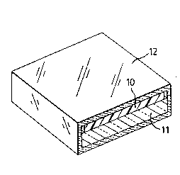
films to permit total internal reflection. Fiyure 12 shows
schematically, in enlarged section, a structure comprising
very many extrinsic light source element~ with enhanced
luminous exitance stacked together to form a composite
radioluminescent source with a large total light output.
In the e~bodiments described above the
radioluminescent light sources are based on the use of thin
films of tritium-occluded amorphous semiconductor.
However, it is to be understood that other radioactive
elements which emit decay betas may be used instead of
tritium. Furthermore, while the matrix can most
conveniently be deposited as a thin film,it will readily be
understood that the matrix may comprise a body of
substantial thickness so long as it is transparent to the
light emitted by the recombination of the electron-hole
pairs. Thus, for example, it is obvious that the
usefulness of the embodiments shown in Figures 4 to 8, and
Figures 11 and 12, in which light is transmitted within the ;
film through a distance far exceeding the film thickness,
depends upon the matrix being essentially transparent
regardless of its thickness.
,'.:
, ,,: :.