Note : Les descriptions sont présentées dans la langue officielle dans laquelle elles ont été soumises.
2 0 6 1 8 5 8
The present invention relates to a raster position
adjusting circuit for controlling a horizontal raster position
of an electromagnetic type cathode ray tube (which will be
referred hereinafter to as a CRT).
An arrangement of a conventional raster position
adjusting circuit includes a first power source Vccl and a
second power source Vcc2, the first power source Vccl being
for the circuit and the second power source Vcc2 being for
supplying a direct current to a horizontal deflecting coil.
The horizontal raster is made by supplying a direct current
to the horizontal deflecting coil and the horizontal right and
left raster position adjustment can be effected by means of
current path systems. The horizontal deflection circuit is
basically composed of the first power source Vccl, a constant-
voltage source, a flyback transformer, the horizontal
deflecting coil, a direct-current blocking capacitor, and a
horizontal output circuit, and additionally equipped with a
choke coil (which prevents the horizontal pulse from being by-
passed), resistors, transistors, a volume and the second power
source Vcc2 in order to change the raster position. A partial
voltage of the second power source Vcc2 due to the position
of a movable contact of the volume is applied to the bases of
both the transistors whereby either the transistors turns ON
in accordance with the applied voltage due to the volume in
relation to the same emitter electric potential so as to
supply a current to the horizontal deflecting coil through the
current path system.
There is a problem which arises such a conventional
raster position adjusting circuit using the volume, however,
in that there is the possibility of lowering its reliability
due to an imperfect connection of the movable contact because
the volume has a mechanical structure, and difficulty is
encountered to easily achieve the automization of the
adjustment of the raster position in the manufacturing process
because of requiring a dedicated device for operation of the
volume. In addition, the position for the provision of the
A~ ~r
206 1 8 58
volume is restricted on the printed circuit board.
It is therefore an object of the present invention
to provide a raster position adjusting circuit which allows
easy automization of the adjustment of the raster position in
the manufacturing process.
According to the present invention, there is
provided a raster position adjusting circuit comprising first
and second voltage sources; a current supply source; a
constant-voltage source; a voltage-controlled type current
lo supply source; a digital-to-analog converter; a flyback trans-
former; a horizontal output circuit; a horizontal deflecting
coil; a direct-current blocking capacitor; and a choke coil,
a voltage supply side of said first voltage source being
coupled to one terminal of said current supply source and
further coupled to one terminal of said constant-voltage
source, the other terminal of said current supply source being
coupled to one terminal of said voltage-controlled type
current supply source and the other terminal of said
voltage-controlled type current supply source being coupled
~o to a grounded side of said first voltage source, said
digital-to-analog converter being coupled to said voltage-
controlled type current supply source so that an output
voltage of said digital-to-analog converter is applied
thereto, a junction point between said current supply source
and said voltage-controlled type current supply source being
connected to one terminal of a first resistor and to bases of
first and second transistors, the other terminal of said first
resistor and emitters of said first and second transistors
being coupled to each other and to an output terminal of said
constant-voltage source, a collector of said first transistor
being coupled to a voltage supply side of said second voltage
source and a collector of said second transistor being coupled
to a grounded side of said second voltage source, one terminal
of a second resistor being coupled to a junction point between
said collector of said first transistor and said second
voltage source and one terminal of a third resistor being
` A
3 206 1 858
coupled to a junction point between said collector of said
second transistor and said second voltage source, the other
terminal of said second resistor and the other terminal of
said third resistor being coupled to each other, one terminal
of a primary side of said flyback transformer being coupled
to the junction point between said emitters of said first and
second transistors and said output terminal of said
constant-voltage source and the other terminal of said primary
side thereof being coupled to said horizontal output circuit,
one terminal of said horizontal deflecting coil being coupled
to a junction point between the other terminal of said primary
side of said flyback transformer and said horizontal output
circuit, and the other terminal of said horizontal deflecting
coil being coupled to one terminal of said direct-current
blocking capacitor, the other terminal of said direct-current
blocking capacitor being coupled to the grounded side of said
first voltage source, one terminal of said choke coil being
coupled to a junction point between said second and third
resistors, and the other terminal of said choke coil being
coupled to a junction point between said horizontal deflecting
coil and said direct-current blocking capacitor.
Preferably, with this circuit in the case of
changing the raster position by supplying direction-different
currents to the horizontal deflecting coil, a different
current between the currents of the current supply source and
the voltage-controlled current supply source flows through the
first resistance provided between the emitters and bases of
the first and second transistors, whereby the first transistor
turns ON and the second transistor turns OFF or the second
transistor turns ON and the first transistor turns OFF. At
this time, since the voltage between the emitters and bases
of the first and second transistors varies in accordance with
the current value flowing through the first resistor, it is
possible to control the current directing from the emitter of
the first transistor to the emitter of the second transistor.
Further, since in this operation the drawing current of the
206 1 858
voltage-controlled type current supply source is controllable
in a range from o to 2I amperes in accordance with the output
voltage of the D/A converter, when the drawing current thereof
is from 0 to a value smaller than I, the different current
between the current due to the current supply source and the
drawing current of the voltage-controlled type current supply
source is introduced into the first resistor, because the
current supply ability I of the first current supply source
is constant, so that the base voltage viewed from the emitter
of the first transistor increases, and hence the first
transistor operates and the second transistor stops to
operate. On the other hand, when the drawing current of the
voltage-controlled type current supply source is I to 2I, the
difference current therebetween is discharged through the
first resistor whereby the first transistor stops to operate
and the second transistor starts to operate.
According to the present invention, there is also
provided a raster position adjusting circuit for use in a
cathode ray tube, comprising:
horizontal deflection means including a deflecting
coil for deflecting an electron beam directed to a screen of
said cathode ray tube;
constant-current supply means for supplying a
constant current;
voltage-controlled type current supply means coupled
to said constant-current supply means and arranged such that
its current is controllable in accordance with an external
voltage signal; and
switching means coupled to a junction point between
said constant-current supply means and said voltage-controlled
type current supply means and further coupled to said
deflecting coil of said horizontal deflection means, said
switching means being arranged so as to control a current
flowing through said deflecting coil in accordance with a
difference current between said constant-current supply means
and said voltage-controlled type current supply means to
`- 206~ 858
adjust a position of a raster on said screen of said cathode
ray tube.
The object and features of the present invention
will become more readily apparent from the following detailed
description of the preferred embodiments taken in conjunction
with the accompanying drawings in which:
Fig. 1 shows an arrangement of a conventional raster
position adjusting circuit; and
Fig. 2 illustrates an arrangement of a raster
position adjusting circuit according to an embodiment of the
present invention;
Fig. 3 is a schematic drawing of a horizontal output
circuit, used in the raster positioning device of Fig. 2;
Fig. 4 is a schematic drawing of a voltage
controlled current supply source used in the raster
positioning device of Fig. 2.
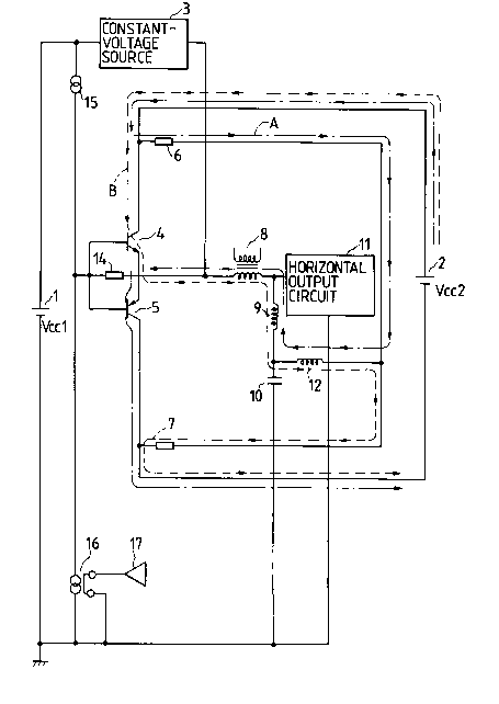
Fig. 1 is an illustration of an arrangement of a
conventional raster position adjusting circuit including a
first power source Vccl designated at numeral 1 and a second
power source Vcc2 designated at numeral 2, the first power
source Vccl being for the circuit and the second power source
Vcc2 being for supplying a direct current to a horizontal
deflecting coil 9. The horizontal raster is made by supplying
a direct current to the horizontal deflecting coil 9 and the
horizontal right and left raster position adjustment can be
effected by means of current path systems indicated by arrows
A (chain line) and B ~dotted line) in Fig. 1. The horizontal
deflection circuit is basically composed of the first power
source Vccl, a constant-voltage source 3, a flyback
transformer 8, the horizontal deflecting coil 9, a direct-
current blocking capacitor 10, and a horizontal output circuit
11, and additionally equipped with a choke coil 12 (which
prevents the horizontal pulse from being by-passed), resistors
6, 7, transistors 4, 5, a volume 13 and the second power
source Vcc2 in order to change the raster position. A partial
voltage of the second power source Vcc2 due to the position
... ~
`` A
206 1 858
_
of a movable contact of the volume 13 is applied to the bases
of both the transistors 4 and 5 whereby either the transistors
4 and 5 turns ON in accordance with the applied voltage due
to the volume 13 in relation to the same emitter electric
potential so as to supply a current to the horizontal
deflecting coil 9 through the current path system indicated
by the arrow A or B.
There is a problem which arises such a conventional
raster position adjusting circuit using the volume 13,
however, in that there is the possibility of lowering its
reliability due to an imperfect connection of the movable
contact because the volume 13 has a mechanical structure, and
difficulty is encountered to easily achieve the automization
of the adjustment of the raster position in the manufacturing
process because of requiring a dedicated device for operation
of the volume. In addition, the position for the provision
of the volume is restricted on the printed circuit board.
Referring now to Fig. 2, there is illustrated an
arrangement of a raster position adjusting circuit according
to an embodiment of the present invention where parts
coresponding to those in Fig. 1 showing the conventional
raster position adjusting circuit are marked with the same
characters and numerals. In Fig. 2, this raster position
adjusting circuit comprises a horizontal deflection circuit
including a power source (Vccl) 1, a constant-voltage source
3 a flyback transformer 8, a horizontal output circuit 11,
a horizontal deflecting coil 9, and a direct-current blocking
capacitor 10. Further, provided are a pair of first and
second transistors 4, 5, first to third
.~
- .a
-7 2061858
,
resistors 14, 6, 7, a choke coil 12 and a power source (Vcc2) 2, thus
basically making up a raster position adjusting circuit which effects
the position adjustment of the horizontal raster on a CRT. More
specifically, this raster position adjusting circuit is first arranged
5 such that the grounded sides of the power sources 1 and 2 is not
coupled to each other. The raster position adjusting circuit is
additionally equipped with a first current supply source (constant-
current supply source) 15 whose current supply ability is I (ampere)
and a voltage-controlled type current supply source (a second
10 current supply source) 1 6 whose maximum current drawing ability
is 2 times the current supply ability I of the first current supply
source 15. The first current supply source 15 is at one terminal
connected to the voltage supply side of the power source 1. The
voltage supply side of the power source 1 is also connected to a
15 constant-voltage source 3. The other terminal of the first current
supply source 15 is connected to one terminal of the voltage-
controlled type current supply source 16, the other terminal of the
voltage-controlled type current supply source 16 being coupled to
the grounded side of the power source 1. The voltage-controlled
20 type current supply source 16 is in a coupling relation to a DA
(digital-to-analog) converter 17 so as to be responsive to the output
voltage thereof.
A junction point between the first current supply source 15
and the voltage-controlled type current supply source 16 is coupled
2 5 to one terminal of the first resistor 14 and further connected to the
2061858
-8 -
bases of the first and second transistors 4 and 5. The emitters of the
first and second transistors 4, 5 and the other terminal of the first
resistor 14 are directly coupled to each other at a coupling point
which is in turn coupled to the output terminal of the constant-
S voltage source 3. The collector of the first transistor 4 is coupled tothe supply side of the power source 2 and the collector of the second
transistor S is coupled to the grounded side of the power source 2.
Further, a junction point between the collector of the first transistor
4 and the power source 2 is connected to one terminal of the second
10 resistor 6, and a junction point between the collector of the second
transistor S and the power source 2 is connected to one terminal of
the third resistor 7. The other terminals of the second and third
resistors 6 and 7 are coupled to each other.
Moreover, one terminal of the primary side of the flyback
15 transformer 8 is connected to a junction point between the emitters
of the first and second transistors 4, 5 and the output terminal of the
constant-voltage source 3, and the other terminal of the primary side
thereof is coupled to the horizontal output circuit 11 whose grounded
terminal is coupled to the grounded side of the power source 1, and a
2 0 junction point between the flyback transformer 8 and the horizontal
output circuit 11 is connected to one terminal of the horizontal
deflecting coil 9, the other terminal of the horizontal deflecting coil 9
being coupled through the direct-current blocking capacitor 10 to the
grounded side of the power source 1. Further, one terminal of the
2 5 choke coil 12 is connected to a junction point between the second and
9 2061858
third resistors 6 and 7 and the other terminal of the choke coil 12 is
connected to a junction point between the horizontal deflecting coil 9
and the direct-current blocking capacitor 10. The choke coil 12 is for
preventing a horizontal pulse from the introduction into the raster
5 position adjusting circuit. With a base voltage viewed from the
emitters of the first and second transistors 4, 5 being applied to the
bases thereof, currents indicated by characters A and B in Fig. 2 flow
through the horizontal deflecting coil 9, thereby allowing the raster
position adjustment.
A base voltage is applied to each of the first and second
transistors 4 and 5 due to a current flowing through the first resistor
14. This base voltage occurs because the difference between the
current of the constant-voltage source 15 having the current supply
ability I (ampere) and the current of the voltage-controlled type
15 current supply source 1 6 having the maximum current drawing
ability 2I is introduced and discharged into and from the first
resistor 14. Here, the drawing current is controllable by the DA
converter 17 in a range from 0 to 2I. Thus, in the case that the
drawing current of the voltage-controlled type current supply source
20 16 is 0 to a value which does not reach I, a portion of the current I of
the constant-current supply source 15 is introduced into the voltage-
controlled type current supply source 16 and the other current
thereof which cannot be introduced thereinto passes through the
first resistor 14, and hence, when viewed from the emitters of the
2 5 first and second transistors 4 and 5, the base voltages of the first and
-lO- 20618~8
second transistors 4 and 5 increase. At this time, since the first
transistor 4 is a NPN transistor and the second transistor 5 is a PNP
transistor, although the second transistor 5 takes the non-energizing
(turning-OFF) state, the first transistor 4 takes the energizing
5 (turning-ON) state whereby the current flows in the direction
indicated by the arrow B in Fig. 2. On the other hand, in the case that
the drawing current of the voltage-controlled type current supply
source 16 is I to 2I, since the current supply ability of the constant-
current source 15 is I, the remaining current flows through the first
10 resistor 14 and therefore, when viewed from the emitters of the first
and second transistors 4 and 5, the base voltages of the first and
second transistors 4 and 5 decrease. Accordingly, the NPN transistor
4 stops to operate and the PNP transistor 5 starts to operate so that
the current flows in the direction indicated by the arrow A in Fig. 2.
15 That is, with the current of the voltage-controlled type current
supply source 16 being controllable by the voltage applied from the
DA converter 17, the base-emitter voltages of the first and second
transistors 4 and 5 vary in accordance with the introduction and
discharge into and from the first resistor 14, whereby it is possible to
2 0 change the direction and value of the deflecting-coil-flowing current
(A, B) to allow the raster position adjustment.
As described above, according to this invention, the electronic
control of the current flowing through the deflecting coil can be
effected with the emitter-base voltages being applied to the first and
2 5 second transistors on the basis of the current between the constant-
20618S8
-1 1-
current supply source and the voltage-controlled type current supply
source which is controllable through the DA converter 17. This
arrangement allows the improvement of the reliability of the circuit
and the computer-based automization unlike the conventional circuit
5 using a mechanical volume.
Fig. 3 shows one example of the above-mentioned horizontal
output circuit 11. This horizontal output circuit is for intermitting
the voltage to the deflecting coil 9 in accordance with the period of
the horizontal frequency 22 so as to supply a sawtooth current to the
10 horizontal deflecting coil 9. As illustrated in Fig. 3, the horizontal
output circuit 11 comprises a drive transformer 21, a horizontal
output transistor 19, a damper diode 20, a direct-current power
source 23 and a resonance capacitor 18. In addition to the supply of
the sawtooth current to the horizontal deflecting coil 9, the horizontal
15 output circuit 11 also has a purpose of supplying a power to the
other circuits by using the flyback pulse generated in its own circuit.
Fig. 4 illustrates one example of the voltage-controlled type
current supply source 16. This voltage-controlled type current
supply source 16 is arranged to vary the current drawing ability in
2 0 accordance with the inputted voltage. In Fig. 4, the voltage-
controlled type current supply source 16 is operated so that the +
input voltage terminal and the - input voltage terminal of an
operational amplifier 24 become equal to each other, and hence the
value of the DC voltage becomes equal to the emitter voltage of a
2 5 transistor, whereby the emitter current having a value of (V/R)
-12- 2061858
flows. V represents the value of the DC voltage and R designates the
value of a resistor 26.
It should be understood that the foregoing relates to only
preferred embodiments of the present invention, and that it is
S intended to cover all changes and modifications of the embodiments
of the invention herein used for the purposes of the disclosure, which
do not constitute departures from the spirit and scope of the
lnvention .