Note : Les descriptions sont présentées dans la langue officielle dans laquelle elles ont été soumises.
wn w rwn-w
.. ... , .. . _...., . Wi ii'v7ii vv rv
-1-
~,1'~'e~1°.;~J~
HIGH DENSITY AND MULTIPLE INSERTION CONN~FCTOR
Backcxround of the Invention
Field of the Invention
The invention relates to high density electrical
connectors and specifically to low insertion force
connectors that are specially suited for repetitive
coupling and uncoupling.
Prior Art
Interconnection of electronic devices such as
integrated circuits and printed circuit boards becomes
increasingly difficult as the number of contacts in-
creases and as the number of times the insertion and
removal of the devices increases. As the number of
°contacts increases, the alignment and the cleanliness
of the contacting surfaces becomes more critical. As
the number of interconnections increases, the potential
for wear and/or damage to the connector through mating
and de-mating becomes greater.
Tt is commonly known to insert a circuit board
into connectors having individual, spring-loaded
retaining contacts in order to provide a removable
connection. As the number of c~ntacts increases, the
amount of force required to overcome the cumulative
resistance~of the corresponding number of ,sockets
v.becomes so great that~the potential for damage to
either the connector or the circuit board becomes far
~~.rv ~~. ..~~5~' .. ..... ...,.~....
~ V/i VVi ~iVV~inV
._ .... .. . '~. ~~..:i.. j '~~il..=;3.... . .. ._... ..... ~.:.
-2-
more likely. The insertion and removal force encoun-
tered is generally borne by the surfaces that are in
rubbing contact during the manipulative step. For ,
example, in U.S. Patent No. 4,826,446 to Juntwait,
individual contact pins having spaced flexible contact
arms are adapted to receive and to be flexed apart by
an electrical component, such as a printed circuit
card, that is inserted and pivoted therein. Although
the connector significantly reduces the amount of force
needed for insertion, the normal forces at the point of
contact on the contact arms 'and on the card nonetheless
eventually cause wear upon each insertion and removal
of the card.
U.S. Patent No. 3,102,767 to Schneck discloses
an electrical connector for flat conductor cable where
the cable is wrapped around a U- or channel-shaped
spring. The dielectric coating of the cable is
stripped to expose the conductor ribbons which are
forced into contact with component boards upon inser-
'20: tion between the arms of the spring: The forces of
insertion and removal in this device are endured by the
conductors and'the contact circuitry on.the surface of
the component boards,. ,U.S: Patent No. 3,319,216 to
McCullough discloses a similar structure wherein multi-
conductor~cable and a printed circuit board are in
rubbing contact with each other upon insertion and
removal of the board:
U:S. Patent No. 3,401,369 to Palmateer et al.
discloses a laminated connector which includes a sheet
of dielectric material and a plurality of electrical.
contact members~far using printed.circuit techniques:
As can bey seen in FIG.. ~ 5 of that . reference, ; the -contact
.»r .::1.,.:. . _. . ».. . , -
pressure between the laminate and the member inserted
therein~is~focused~on~conductive members on the inser-
wn n~ W non
" .. ' -. --__' . . .-.~ ~ 7l~:vv....~
.. ..._ . . ... . _ . ... .. .z ~,~.,; .. _.... .. ,
-3- .~ a 4 Ct .,l ~t
tion member and on contact buttons on the laminate. -
Such a construction will have limited multiple inser-
tion and removal life. To overcome problems of
alignment and insertion force, electrical connectors
have been developed which use mechanical actuation to
close (or open) contacts and to maintain a mechanical
retaining force. Such devices are generally complex
and bulky. More sophisticated actuation mechanisms
using shape-memory alloy actuators have also been
l0 developed in which remote electrical actuation of the
connector is provided.
None of the above-discussed connectors provides
a concept for a simple, manually-operated, low inser-
tion force, high density, multiple insertion connector
with independent two-sided contact and contact wiping
for a wide range of connector configurations, such as
those discussed above, including connectors which
provide for remote electrical actuation.
&ummarv of the Invention
~ The purpose of the invention is to provide a
high density, low insertion force connector design that
y minimizes, the amount of friction created by insertion
and:withdrawal of a male portion with respect to a
female portion while simultaneously providing wiping
and~high contact force between electrical contacts on
each portion,.in.a;variety of overall connector-configu-
rations.. To,accomplish this purpose there is provided .
a connector having,a female portion with a generally C-
shaped biasing member: and flexible circuitry mounted
about, the biasing member. Thewcircuitry has electrical
contacts 'positioned near and: lightly spaced from the
ends~of the biasing member, the flexible circuitry near
the 'electrical contacts generally having a sliding
.. ... . .. . .....~ i'i: ii % i ~ ~=i i i iiii i'<.ii
. . ... _ . ,..~q.~~J~,;~, ";i ....~..... _ .. .....
-4-
surface. The connector also includes a male portion
having an insertion member insertable within the
flexible circuitry, the male portion having contacts .
positioned adjacent to but spaced from the edge of the
insertion member and also generally having sliding
surfaces above and below the contacts, the sliding
surfaces contacting each other and being made from
materials which minimize the amount of friction created
upon contact by repeated insertion and withdrawal of
the insertion member relative to the~flexible circuit-
ry. Further insertion movement of the insertion member
provides wiping and positioning of all of the contacts
of both portions into mating position.
In one aspect of the invention there is provided
a high density multiple insertion connector comprising:
a biasing member, said biasing member being
elongated and having a longitudinal opening along the
length thereof; said biasing member being generally C-
shaped and having a center portion and arm portions
having ends;
flexible circuitry having first and second sets
of parallel-spaced electrical conductors, at least a
portion of said flexible circuitry mounted about said
biasing member, said electrical conductors terminating
in first and second sets of electrical contacts, said
first set of contacts. positioned on one side of said
opening and said second set of contacts positioned on
the other side of said opening, said first and second
sets of electrical contacts positioned within the
opening near but slightly spaced from the ends of said
arm'portions, the flexible circuitry near said first
and second sets of electrical contacts having a first
sliding surface, said biasing member and said flexible
circuitry defining a female portion of the connector:
and
i ~ ~ i t % I ! V J a V ~ ' i vw V 1 % I i 11 ~ s i 1
-5- 1~' l9 ~ e'~ ,i i3 ti -.
an insertion member, said insertion member being
elongated and having a longitudinal edge for insertion
into said opening, said insertion member having addi-
tional flexible circuitry on the surface thereof
including third and fourth sets of parallel-spaced con-
ductors, said third and fourth sets of conductors
positioned on each side of said insertion member, said
third and fourth sets of electrical conductors ter-
minating in third and fourth sets of electrical
contacts positioned adjacent to but spaced from the
edge of said insertion member, the flexible circuitry
near said third and fourth sets of electrical contacts
having a second sliding surface, said first and second
sliding surfaces being made of low friction material
such that insertion or removal of the insertion member
causes contact between said first and second surfaces,
overcoming the bias of said biasing member ~o widen the
opening further for insertion or withdrawal of the
insertion member, said first and second surfaces
undergoing a minimum of friction created by insertion
and removal of the insertion member, further insertion
movement of the insertion member positioning and wiping
the contacts of said first, second, third, and fourth
sets of electrical contacts with respect to each other
'25 into mating position, the insertion member defining a
male portion of the connector.
pescribtion of the Drawing
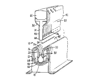
FIG. 1 is an exploded partial perspective view
of the connector of the invention with the insertion
member positioned prior to insertion. The Figure also
illustrates an optional..shape-memory alloy element and
heater positioned within the biasing member to provide
remote electrical.actuation for true zero insertion
force if desired. .
"". .,. ,.
.. .. _ ., ......, . ~ '.W:W iiav:l::
_ .: ". ~, ;' .. -: .
yn.: i .;, . . . _6_
FIG. 2 is a cross-sectional view of the connec-
tor of the invention with the insertion member fully
inserted and further including an environmental
shield/housing.
FIG. 3 is a partial enlarged view of the mating
portions of the insertion member and the flexible
circuitry including the ends of the biasing member.
FIG. 4 is a partial cross-sectional view of the
contact area of one side of the female portion of the
la connector of the invention illustrating the arm portion
of the biasing member and the typical layered construc-
tion of the flexible circuitry.
FIG. 5 is a partial cross-sectional view similar
to FIG: 4 of the contact area of one side of the male
portion of the connector of the invention illustrating
the typical layered construction of the flexible cir-
cuitry.
FIG. 6 is a partial rotated view of one side of
the male and female portions of the connector illus-
trating the contact zones of each portion which allow
for alignment mismatch.
FIG. 7 is a partial view perpendicular to the
contact zones of the male and female portions of the
connector illustrating the relative preferred widths of
the contacts.
~escrintion of the Preferred ESnbodiments
...,.z , . .. . : .
With continued reference to the drawing, FIG. l
illustrates a high density multiple insertion connec-
a'vi~iliivi.i~ W iiiiW 9iia~iii.
- ... _. - - .... ... . : . ,-, ~ :E ,- : a . . . ~ . - : . . ~... .
_.... ..~ -~ ;.. .:.~r _
-?-
tor, shown generally at 10. Connector 10 includes a
female portion 12 and a male portion 14, each portion
having a high density of generally parallel-spaced
electrical conductors terminating in contacts.
Female portion 12 includes biasing member 16
which is elongated and has a longitudinal opening along
the length thereof, biasing member 16 being generally
C-shaped and having a center portion l8 and arm por-
tions 2o terminating in the opening. Biasing member 16
is made from spring material, preferably beryllium
copper or other suitable materials.
Biasing member 16 is shown to have arm portions
which extend within the overall C-shape of biasing
member 16. As seen in FIG. 3 in phantom line, it is
15 within the scope of the invention to have alternative
arm portions 22 which extend only outwardly rather than
inwardly. In such an embodiment, alternative arm por-
tions 22 extend outwardly and curve at the ends'thereof
to likewise accommodate the bending of flexible'cir-
20 cuitry which would hang-over the ends of the arm por-
tions in drape-like fashion. It is further within the
scope of the invention to have connector configurations
'with female portion biasing members of various aonfigu-
rations of arm members, lengths, and angular orienta-
tions so long as such arm portions and the flexible
circuitry mounted thereon are moved by-insertion of a
-maleportion to connect or disconnect the two portions
of the connector.
Female portion 12 also includes flexible
circuitry 24 having first and second sets of parallel-
~.' ~ paced ~lectricalwconductors 26 and 28'rrespectively,
.at least a portion of flexible circuitry-'24 being
mounted about'biasing member 16. A typical layered
w r : :. ; : a:,::
i7 1l;IIi %IIIIA'i11
:~~r ~~ o,~ - _.. .. . .. -
17 5 ~"' ~ '~
-g-
construction of flexible circuitry 24 is shown in FIG.
4, which will be described later in further detail. It
is understood that it is within the scope of the inven-
tion to use various constructions of flexible circuitry
mounted about biasing member 16. As shown in FIGS. 1
and 3, first and second sets of parallel-spaced
electrical conductors 26 and 28, respectively, are
mounted about arm portions 20. The individual conduc-
tors of first and second sets of parallel-spaced
electrical conductors 26 and 28,, respectively, are.
oriented generally perpendicular to the opening in
biasing member 16.
The electrical conductors of first and second
sets of parallel-spaced electrical conductors.26 and
28, respectively, terminate in first and second sets of
electrical contacts 30 and 32, respectively, the first
set of electrical contacts 30 positioned on one side of
said opening, and the second set of electrical contacts
32 positioned on the other side of the opening, said
first and second sets of electrical contacts 30 and 32,
respectively, positioned within the opening near but
slightly spaced from the ends of said arm portions 20.
The area of flexible circuitry 24 near the contacts,
especially above the electrical contacts (taken along
the line of insertion) is defined as first sliding
surface 31. .In FIG. 3, the approximate center of
contact for first and second sets of electrical con-
tacts 30.;,and,32, respectively, is generally dissected
by a plane having a center line 34. It can be seen
that center line 34 is near but slightly spaced from
the ends.of arm portions 20.
.,' Male portion,l4 of connector 10 comprises an
insertion member 15, insertion member 15 being elongat-
e~d and having a longitudinal edge 36 for insertion into
~
~ \ 1 7 1 I~ 1 1 71,77 YI 1 % 1 ~~V i iiilt 1 %11
-
the opening of female portion 12. Insertion member 15
has flexible circuitry 38 on the surface thereof
including third and fourth sets of parallel-spaced
electrical conductors 40 and 42, respectively. Third
. 5 and fourth sets of parallel-spaced electrical conduc-
tors 40 and 42, respectively, are also oriented perpen-
dicular to the opening. Third and fourth sets of
parallel-spaced electrical conductors 40 and 42,
respectively, are complementary with first and second
sets of parallel-spaced electrical conductors 26 and
28, respectively. Positioned on each side of insertion
member 15, third and fourth sets of parallel-spaced
electrical conductors 40 and 42, respectively, termi-
nate in third and fourth sets of electrical contacts 44
and 46, respectively. Third and fourth sets of
electrical contacts 44 and 46, respectively, are posi-
tinned adjacent to but spaced from longitudinal edge 36
of insertion member 15. Flexible circuitry 38 has a
second sliding surface 45 near third and fourth sets of
electrical contacts 44 and 46, respectively, which can ,,
clearly be seen in FIG. 5, each of at least the first
and second sliding surfaces 31 and 45, respectively, of
the flexible circuitries 24 and 38 having a layer of '
similar dielectric and low friction material on the
outsides thereof in the defined areas which rub against
each other upon insertion and removal movement of the
connector portions.
In FIGS.:3, 4 and 5, flexible circuitry 24'of
female portion 12 and flexible circuitry 38-of male
portiow:l4~-.include layers 25 ,33, and 35 of dielectric
material, such as KaptonTr'~, having first-and second
sets of parallel-spaced electrical conductors 26 and
28, respectively,w'and third and fourth sets of'paral-
lel-spaced electrical~conductors 40 and 42, respective-
ly, insulated therein.
vs:i ~:._. _ _.._.. .'~,:l; L'7'.-'!!1'lD~.'!.~
...... .' ;:,.,'; .~;.. ~. i~'.,,; _ ~ . . ..~ . .. . ._.. '.._
._ .. ..
-10-
In FIG. 4, the preferred layered structure of
flexible circuitry 24 is shown in cross-section mounted
on biasing member 16. First and second sets of paral-
lel-spaced electrical conductors 26 and 28, respective-
ly, are preferably made from copper with the contact
zones plated with nickel and followed by gold on the
surface. Layers of dielectric material 25 are posi-
tioned over and under first set of parallel-spaced
electrical conductors 26; a portion of the outer layer
of dielectric material 25, especially above the elec-
trical contacts, comprises first sliding surface 31.
Copper ground plane 27 is positianed below inside layer
of dielectric material 25 and is attached to biasing
member 16 by adhesive Layer 29.
It is understood that it is within the scope of
the invention to use types of flexible circuitry other
than that described above with respect to both the male
and female portions of the connector.
In FIGS. 1, 3 and 5, the preferred layered
structure of flexible circuitry noted generally at 38
is mounted on insertion member 15 which is made of
aluminum, liquid crystal polymer, stainless steel, or
polyether-ether-ketone. Third and fourth sets of
electrical contacts 44 and 46, respectively, have a
gold surface with a nickel-plated barrier over copper
conductors 40 and 42 which are sandwiched between
layers of~dielectric material 33 and 35 such as those
used for., layers of, dielectric material 25. Outer layer
of dielectric material 33 in the area especially noted
at .second sliding surface 45 comprises second sliding
surface 45. It can be seen that second sliding surface
45,essentially surroundsthird,and fourth sets of
electrical contacts 44 and..46, respectively, with layer
of dielectric material 33 an each side of third and
i~l.% 71% 1~117J Y. A % i 1\~71 %1~111%1
-11_ l.~,di ;i z? ;-: 'r; sj
fourth sets of electrical contacts 44 and 46,
respectively. Copper ground plane 37 is positioned
below layer of dielectric material 35 and is attached
to insertion member 15 by adhesive layer 39.
Although first and second sliding surfaces 31
and 45, respectively, disclosed are made of KaptonTM,
it is understood that these surfaces may be made of any
low friction material, including TeflonTM.
With continued reference to FIG. 3, upon inser-
tion of male portion 14, outer surface 45 below center
line 54 (earlier defined as second sliding surface 45)
contacts the outside layer 48 of female portion 7.2
above center line 56 (earlier defined as first sliding
surface 31). It can be seen that further movement of
the generally bulbous-shaped male portion 14 spreads
the arm portions 20 and causes sliding contact between
the first and second surfaces of similar materials.
The similar materials minimize the amount of friction
created by inserting male portion 14 to the point along
the line of insertion at which first and second sets of
electrical contacts 30 and 32, respectively, mate with
third and fourth sets of electrical contacts 44 and 46,
respectively. The bulbous shape created by second
sliding surface 45 can be exaggerated by, for example,
narrowing the thickness of male portion 14, such as at
point 52, to obtain mechanical advantage in prying the
arm portions 20 apart. The bulbous shape and the angle
of the arm portions 20 relative to the angle of inner-
' tion decrease the friction forces parallel to the first
sliding surface 3l until the, point where the second
sliding surface 45. clears the contacts 30 and 32 where
the arm portions,20 can move back toward each other,
changing their relative angle to each other, becoming
essentially parallel and increasing the amount of
W 1 i v 1 % 1 111 ~~ ~ 11. ~ 1 i 1 I~ ~I; i v~~ i,~inl
-12-
normal force to its maximum to wipe the contacts with
respect to each other and to maintain electrical con-
tinuity in operation. Upon contact between all of the
electrical contacts, a small amount of further movement
indicated by dimension 58 positions and wipes and .
cleans the contacts of the first, second, third, and
fourth sets of electrical contacts 30, 32, 44, and 46,
respectively.
Upon removal of male portion 14, outer surface
45 of male portion I4 below center line 54 first cpn-
tacts the surfaces at the first and second sets of
electrical contacts 30 and 32, and then contacts out-
side layer 48 of female portion 12 above center line
56. It can be seen, therefore, that insertion and
removal of male portion 14 with respect to female
portion 12 is accomplished with a minimum amount of
friction and without excessive wear to the electrical
contacts or electrical conductors of the respective
flexible circuitries.
In FIG. 1 it can be seen that male portion 14 is
attached to a printed circuit baard (daughter board
60): It is understood that male portion 14 may be
integral with daughter board 60.
Also, the flexible circuitry tail end of the
male portion is adapted to surface mount to the printed
circuit board by reflow soldering or single point
bonding:: Because printed circuit boards are often not
made to the precision of flexible circuitry, the design
of the flexible circuitry tail end of the male portion
can be made to flare out or to use a grid pattern of
contacts, thus making alignment an easy match to the
printed circuit board.
iW i'~ii~~ laijy ' isui iu~~ iiy
. ::.; L... L..,._
M~ ''~ '.J t~,
1 7
-lg- N -.v :. ~ ,..: :.
In FIG. 2 it can be seen that flexible circuitry
24 may be electrically connected to a printed circuit
board (mother board 62). Connector 10 of the invention
is not limited by the particular means of electrical
connection of flexible circuitry 24 to mother board 62,
as various types of permanent connection are known in
the art.
FIG. 1 illustrates an optional shape-memory
alloy element 64 having a heater 66 positioned between
shape-memory alloy element 64 and biasing member 16.
Shape-memory alloy element 64 and heater 66 are of the
type described fully in commonly-assigned U.S. Patent
No. 4,881,908 to Perry et al. which is incorporated
herein by reference. It is understood that it~ is
within the scope of the invention to heat shape-memory
alloy element 64 by passing electrical current through
it (resistance heating). This option would then create
true zero insertion (make-break) forces but would still
allow the Iow insertion force functions as desired.
FIGS.,6 and 7 illustrate the advantage of making
the male contacts narrower than the female contacts (or
vice versa). The narrower contact can misalign on the
other contact by an amount ~ Y~ and still make full
electrical contact between the elements.
Environmental and dust shield 63 (shown in FIG.
2) installed on the male member and sealing on a
polymeric seal 68 on the female side is an optional
feature of connector 10.
From the foregoing detailed description, it is
evident that there are a number of changes, adapta-
tions, and modifications of the present invention which
come within the province of those skilled in the art.
~i i ~ i i s : __ _ vi Tl7~TC'v: i:,:,i.:v
._. _ . _ . . ... . .. ., :~ n ', ; ~; ~ a _ , , .
.1Y "
-14-
However, it is intended that all such variations not
departing from the spirit of the invention be consid-
ered as being within the scope thereof and as being
limited solely by the appended claims.