Sélection de la langue

Search

Sommaire du brevet 2077285 

Énoncé de désistement de responsabilité concernant l'information provenant de tiers

Une partie des informations de ce site Web a été fournie par des sources externes. Le gouvernement du Canada n'assume aucune responsabilité concernant la précision, l'actualité ou la fiabilité des informations fournies par les sources externes. Les utilisateurs qui désirent employer cette information devraient consulter directement la source des informations. Le contenu fourni par les sources externes n'est pas assujetti aux exigences sur les langues officielles, la protection des renseignements personnels et l'accessibilité.

Disponibilité de l'Abrégé et des Revendications

L'apparition de différences dans le texte et l'image des Revendications et de l'Abrégé dépend du moment auquel le document est publié. Les textes des Revendications et de l'Abrégé sont affichés :

  • lorsque la demande peut être examinée par le public;
  • lorsque le brevet est émis (délivrance).
(12) Demande de brevet: (11) CA 2077285
(54) Titre français: METHODE DE FABRICATION DE DISQUES DE MEMOIRE OPTIQUES
(54) Titre anglais: METHOD FOR MANUFACTURING ROM TYPE OPTICAL DISK
Statut: Réputée abandonnée et au-delà du délai pour le rétablissement - en attente de la réponse à l’avis de communication rejetée
Données bibliographiques
(51) Classification internationale des brevets (CIB):
  • G11B 07/26 (2006.01)
  • G11B 20/10 (2006.01)
  • G11B 20/12 (2006.01)
(72) Inventeurs :
  • FURUKAWA, YASUHITO (Japon)
  • DEGUCHI, TOSHIHISA (Japon)
  • KAMI, KENICHIRO (Japon)
(73) Titulaires :
  • SUMITOMO CHEMICAL CO., LTD.
  • SUMITOMO METAL INDUSTRIES, LTD.
(71) Demandeurs :
  • SUMITOMO CHEMICAL CO., LTD. (Japon)
  • SUMITOMO METAL INDUSTRIES, LTD. (Japon)
(74) Agent: SMART & BIGGAR LP
(74) Co-agent:
(45) Délivré:
(22) Date de dépôt: 1992-09-01
(41) Mise à la disponibilité du public: 1993-03-11
Licence disponible: S.O.
Cédé au domaine public: S.O.
(25) Langue des documents déposés: Anglais

Traité de coopération en matière de brevets (PCT): Non

(30) Données de priorité de la demande:
Numéro de la demande Pays / territoire Date
03-230442 (Japon) 1991-09-10

Abrégés

Abrégé anglais


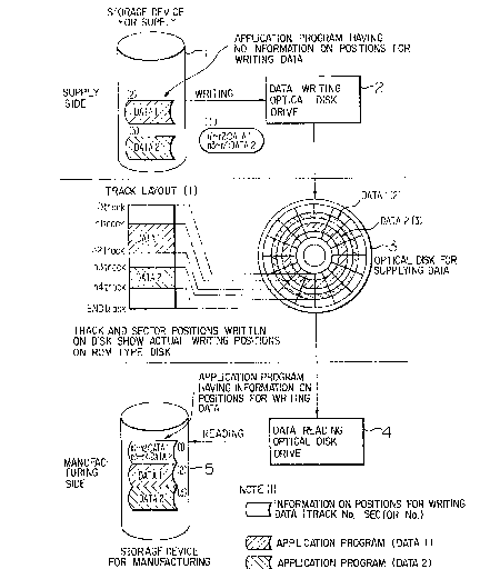
ABSTRACT OF THE DISCLOSURE
According to the present invention, there is
provided a method for manufacturing a ROM type optical
disk in which application program data are written,
wherein application program data having no information
on positions for writing data stored in a storage device
are written in an optical disk for supplying data by a
data writing optical disk drive, and then, the
application program data and information on positions
for writing data are read out of an optical disk for
supplying data by a data reading optical disk drive and
stored in a storage device for manufacturing a ROM type
optical disk.

Revendications

Note : Les revendications sont présentées dans la langue officielle dans laquelle elles ont été soumises.


Claims
1. A method for manufacturing a ROM type optical
disk in which application program data are written,
comprising the steps of:
application program data having no information
on positions for writing data stored in a storage device
are written in an optical disk for supplying data by a
data writing optical disk drive; and then
reading application program data and
information on positions for writing data out of an
optical disk for supplying data by a data reading
optical disk drive and stored in a storage device for
manufacturing a ROM type optical disk.
2. A method for manufacturing a ROM type optical
disk according to Claim 1, wherein the storage devices
are hard disks, optical disks or tape streamers.
3. A method for manufacturing a ROM type optical
disk according to Claim 1, wherein the optical disk for
supplying data is a write-once type or erasable type
optical disk.

Description

Note : Les descriptions sont présentées dans la langue officielle dans laquelle elles ont été soumises.


2~7728~
1 BACKGROUND OF THE INVENTION
The present inven~ion rPlates to a me~hod for
manufacturing a ROM type optical disk, and more
particularly to a method for obtaining application
S program data for writing in a ROM type optical disk
added with information on data writing positions showing
track and sector arrangement and the like in the
manufacture of -the ROM type optical disk~
There are those types of optical disks called
ROM and Partial-ROM (P-ROM). These are of such a type
that application program data are recorded in the whole
(ROM) or a part of (P-ROM) optical disk in advance, and
a general user can execute and mak~e access to the
application program data recorded on an optical disk
without writing the application program data in the
optical disk by oneself.
As the features of this ROM type optical disk,
such points may be mentioned that a sheet of stamper for
forming in which application program data are written is
manufactured and several thousand sheets of ROM type
optical disks are manufactured by resin molding using
this stamper, thereby enabling to supply ROM type
optical disks in which application program data are
written to a plurality of users at a low price.
-- 1 --

2~7728~
1 SU~MARY OF THE INVENTION
Here, in order to manufacture a stamper for
forming in which application pxogram data are written
while accommodating quickly, a supply configuration of
S data becomes a primary factor when the application
program data are supplied. As of now, however, the ROM
type optical disk is not on the market, and definite
techniques related to the supply configuration have
neither been established at present.
It is an object of the present invenkion to
convert application program data having no information
on positions for writing supplied data into application
program data having inforrnation on positions for writing
data easily and promptly.
Namely, according to the present invention,
there is provided a method for manufacturing a ROM type
optical disk with application program data written
therein, wherein application program data having no
information on positions for writing data stored in a
storage de~ice are written in an optical disk for
supplying data by a data writing optical disk drive, and
then application program data and information on
positions for writing data are read out of the optical
d~sk for ~upplying data by a data reading optical disk
drive and stored in a storage device for manufacturing a
ROM type optical disk.
The application program data having no
information on positions for writing the data stored in

2~7728~
1 the storage d~vice for supplying an application program
are written in an optical disk for supplying data using
an optical disk drive for writing data so as to show a
layout (track and sector axrangement) same as that of a
ROM type optical disk to be manufactured.
Next, th~ optical disk for supplying data in
which this application program data are writtPn is read
by means of an optical disk drive for reading the data
so as to store information on positions for writing the
data showing application program data, track and sector
arrangement and the like in the storage device for
manufacturing a ROM type optical disk.
The application program having writing
information stored in the storage unit ~or manufacturing
a RO~ type optical disk is modulated and recorded on a
glass original plate applied with photoresist by means
of a formatter and a cutting machine in accordance with
an established rule, a stamper is produced, resin
molding is performed with this sta~lper and a recording
layer and/or a reflective layer and ~he like are coated
thereon, thus manufacturing a ROM type optical disk.
Besides, the storage device may be any of
these that can execute input/output of data such as a
hard disk, an optical disk and a tape streamer.
Further, a write-once type or erasable type optical disk
is used for the disk for supplying the data. Since
rewriting of the data in the optical disk is possible
when an erasable type optical disk is used, it is

2~1772~
1 possible to use the same optical disk any number of
times for supplying the application program data.
BRIEF DESCRIPTION OF THE DRAWING
Fig. 1 is a diagram showing a flow of data
supply for manufacturing a ROM optical disk according to
the present invention.
DESCRIPTION OF PREFERRED EMBODIMENT
An embodiment of the present invention is
shown in Fig. 1.
Application program data [2] and [3] to be
written into a ROM type disk are stored in a storage
device 1 consisting of a hard disk for supplying
application program data. These application program
data have no information on track arrangement in a disk.
Application program data are written in an
optical disk for supplying data. An erasable type
optical disk 3 for supplying data is set to a data
writing optical disk drive 2 so as to be brought to a
writable state. The application program data stored in
the storage device 1 in this state are written in the
optical disk 3 for supplying data in accordance with
information ~1] on the writing positions such as track
and sector arrangement so as to show the same
arrangement as that in a ROM type optical disk to be
manufactured.
In the optical disk 3 for supplying data

~77~
1 produced here, the track and sector arrangement and the
like have the same layout as that of the produced ROM
type optical disk, and the actual respective track and
sector positions on the optical disk show the writing
positions of the application program data. Further, the
data at respective positions become the actual
application program da~a that are written i.n the ROM
type optical disk.
Nex~, the data that are written in the optical
disk are read out of the optical disk 3 for supplying
the data by a data reading optic l disk drive 4. The
reading positions (track and sector positions) of the
data which ~re being read at ~his time are acquired by
the drive. The appli~ation program data [2] and [3
read out by the drive to a storage device 5 for
manufacturiny a ROM type optical di~k and the
information [1] on positions for writing the data
showing the track and sector arrangement at that time
are stored in a storage device 5 for manufacturing a ROM
t~pe optical disk.
~ ith this, it is possible to obtain an
application program for writing in a ROM type disk in
which the information [1] on positions for writing the
data showing the track and sector arrangement is added
to the application programs [2] and [33 for writing in a
ROM type disk in a storage device for manufacturing.
~ ccording to a method of the present
invention, it is possible to convert application program

2~7728~
1 data having no information on positions for writing the
data showing the track and sector arrangement and the
like into application program data for writing in a ROM
type optical disk added with information on positions
S for writing the data showing the track and sector
arrangement and the like easily and promptly.
;`i; .

Dessin représentatif
Une figure unique qui représente un dessin illustrant l'invention.
États administratifs

2024-08-01 : Dans le cadre de la transition vers les Brevets de nouvelle génération (BNG), la base de données sur les brevets canadiens (BDBC) contient désormais un Historique d'événement plus détaillé, qui reproduit le Journal des événements de notre nouvelle solution interne.

Veuillez noter que les événements débutant par « Inactive : » se réfèrent à des événements qui ne sont plus utilisés dans notre nouvelle solution interne.

Pour une meilleure compréhension de l'état de la demande ou brevet qui figure sur cette page, la rubrique Mise en garde , et les descriptions de Brevet , Historique d'événement , Taxes périodiques et Historique des paiements devraient être consultées.

Historique d'événement

Description Date
Inactive : CIB de MCD 2006-03-11
Le délai pour l'annulation est expiré 1995-03-01
Demande non rétablie avant l'échéance 1995-03-01
Réputée abandonnée - omission de répondre à un avis sur les taxes pour le maintien en état 1994-09-01
Inactive : Demande ad hoc documentée 1994-09-01
Demande publiée (accessible au public) 1993-03-11

Historique d'abandonnement

Date d'abandonnement Raison Date de rétablissement
1994-09-01
Titulaires au dossier

Les titulaires actuels et antérieures au dossier sont affichés en ordre alphabétique.

Titulaires actuels au dossier
SUMITOMO CHEMICAL CO., LTD.
SUMITOMO METAL INDUSTRIES, LTD.
Titulaires antérieures au dossier
KENICHIRO KAMI
TOSHIHISA DEGUCHI
YASUHITO FURUKAWA
Les propriétaires antérieurs qui ne figurent pas dans la liste des « Propriétaires au dossier » apparaîtront dans d'autres documents au dossier.
Documents

Pour visionner les fichiers sélectionnés, entrer le code reCAPTCHA :


Pour visualiser une image, cliquer sur un lien dans la colonne description du document. Pour télécharger l'image (les images), cliquer l'une ou plusieurs cases à cocher dans la première colonne et ensuite cliquer sur le bouton "Télécharger sélection en format PDF (archive Zip)" ou le bouton "Télécharger sélection (en un fichier PDF fusionné)".

Liste des documents de brevet publiés et non publiés sur la BDBC .

Si vous avez des difficultés à accéder au contenu, veuillez communiquer avec le Centre de services à la clientèle au 1-866-997-1936, ou envoyer un courriel au Centre de service à la clientèle de l'OPIC.


Description du
Document 
Date
(aaaa-mm-jj) 
Nombre de pages   Taille de l'image (Ko) 
Revendications 1993-03-10 1 26
Dessins 1993-03-10 1 40
Abrégé 1993-03-10 1 17
Description 1993-03-10 6 178
Dessin représentatif 1999-06-15 1 35