Sélection de la langue

Search

Sommaire du brevet 2080479 

Énoncé de désistement de responsabilité concernant l'information provenant de tiers

Une partie des informations de ce site Web a été fournie par des sources externes. Le gouvernement du Canada n'assume aucune responsabilité concernant la précision, l'actualité ou la fiabilité des informations fournies par les sources externes. Les utilisateurs qui désirent employer cette information devraient consulter directement la source des informations. Le contenu fourni par les sources externes n'est pas assujetti aux exigences sur les langues officielles, la protection des renseignements personnels et l'accessibilité.

Disponibilité de l'Abrégé et des Revendications

L'apparition de différences dans le texte et l'image des Revendications et de l'Abrégé dépend du moment auquel le document est publié. Les textes des Revendications et de l'Abrégé sont affichés :

  • lorsque la demande peut être examinée par le public;
  • lorsque le brevet est émis (délivrance).
(12) Demande de brevet: (11) CA 2080479
(54) Titre français: METHODE DE FABRICATION D'UNE AMORCE DE BANDE MAGNETIQUE A PELLICULE MINCE
(54) Titre anglais: PROCESS FOR PRODUCING A THIN-FILM MAGNETIC TAPE HEAD
Statut: Réputée abandonnée et au-delà du délai pour le rétablissement - en attente de la réponse à l’avis de communication rejetée
Données bibliographiques
(51) Classification internationale des brevets (CIB):
  • G11B 05/31 (2006.01)
(72) Inventeurs :
  • UHDE, DIETMAR (Allemagne)
(73) Titulaires :
  • DEUTSCHE THOMSON-BRANDT GMBH
(71) Demandeurs :
  • DEUTSCHE THOMSON-BRANDT GMBH (Allemagne)
(74) Agent: SMART & BIGGAR LP
(74) Co-agent:
(45) Délivré:
(86) Date de dépôt PCT: 1991-04-15
(87) Mise à la disponibilité du public: 1991-10-24
Licence disponible: S.O.
Cédé au domaine public: S.O.
(25) Langue des documents déposés: Anglais

Traité de coopération en matière de brevets (PCT): Oui
(86) Numéro de la demande PCT: PCT/EP1991/000713
(87) Numéro de publication internationale PCT: EP1991000713
(85) Entrée nationale: 1992-10-13

(30) Données de priorité de la demande:
Numéro de la demande Pays / territoire Date
P 40 12 823.7 (Allemagne) 1990-04-23

Abrégés

Abrégé anglais

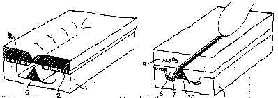
2080479 9116703 PCTABS00008
There is no known feasible way of producing a true thin-film
magnetic tape head with azimuth. A gap inclination (azimuth) can be
made only by mechanically machining the substrate. The aim of the
invention is to produce a thin-film magnetic tape head without
putting two half-blocks together. According to the invention, a
thin-film magnetic tape head (1, 6, 7, 8, 9) is produced in fifteen
process stages in which the "hour-glass effect" is of prime
importance. The process of the invention for producing a thin-film
magnetic tape head combines the advantages of planar thin-film
technology and gap production with the magnetic and mechanical
advantages of conventionally manufactured heads. Magnetic tape devices,
especially video recorders.

Revendications

Note : Les revendications sont présentées dans la langue officielle dans laquelle elles ont été soumises.


- 5 - PCT/EP91/00713
P a t e n t C l a i m s
1. Process for producing a thin-film magnetic tape
head, c h a r a c t e r i z e d b y the following
steps:
a) A substrate (1) (wafer) is provided with a
coating (layer) (2) which is resistant to a caustic
medium for the substrate (1).
b) A window (3) is etched into the layer (2).
c) A cavity (4) is etched into the substrate (1)
through the window (3).
d) A magnetic material (5) (e.g. Sendust) is
deposited on to the substrate (1), whereby in the
cavity (4), a prismoid (6) formed as a gusset (wedge)
projecting upwards ensues.
e) The layer (2) and the magnetic material (5)
deposited thereon are removed, for example, by
stripping.
f) The substrate (1) is etched away so far from
both sides of the prismoid (6) until the prismoid
projects out of the substrate surface.
g) The substrate (1) is provided with a layer which
serves as a gap coating (7).
h) By using asymmetric etching, for example, by
inclining the wafer or the etching device, the gap
layer (7) is partly removed, whereby the gap layer
remains on one side of the prismoid (6).

- 6 - PCT/EP91/00713
i) A further layer (8), consisting of a magnetic
material (e.g. Sendust), is deposited on to the
substrate (1).
j) Various parts of the magnetic tape head, for
example, pole shoes, winding space, etc., are shaped
by etching in the further layer (8).
k) The substrate (1) is polished, whereby the
prismoid apex (gusset apex) is removed.
l) Head windings are manufactured in thin-film
technology which form the head legs of the thin-film
magnetic tape head.
m) A further magnetic layer is deposited and this
produces a return path for the head windings.
n) The substrate is provided with a further layer
(9), for example, a metal oxide such as AL2O3, and
thereby protected.
o) The wafer is divided, ground and polished.
2. Process according to claim 1, c h a r a c t e r -
i z e d i n t h a t the prismoid is completely
raised out of the substrate.
3. Process according to claim 1, characterized is that
the window 3 is etched using a photographic or
photolithographic technique.
4. Process according to claim 1 or 3, c h a r -
a c t e r i z e d i n t h a t the window (3) is
rectangular-shaped.

- 7 - PCT/EP91/00713
5. Process according to claim 1 or 2, c h a r -
a c t e r i z e d i n t h a t the prismoid is
formed as a prism.
6. Process according to claim 1, c h a r a c t e r -
i z e d i n t h a t the magnetic materials (5, 8)
are formed as soft magnetic materials.

Description

Note : Les descriptions sont présentées dans la langue officielle dans laquelle elles ont été soumises.


r~ ~ PCT/EP91/00713
Proces~ for producing a ~hin-film magnetic tape head
There is no promising approach known for manufacturing a
true thin-film magnetic tape head with azimuth. ~nown
metal-in-gap (e.g. Sony TSS, etc.) or lamelIar sendu~t-
amorphous head~ are manufactured in blocks (non-planar) and
the formation of ths air gap is carried out via through the
putting together of two half-blocks. Thin-film blocks like,
for example, the IMB Spiral ~ard Disk head, is, owing to the -
small gap height, not suitàble for systems with tape-head
contact as is required in magnetic tape devices.
A gap inclination (azimuth) can only be generated
I through mechanically machining the backing material
j (substrate).
- ..*
Apart from that, such a type of magnetic tape head
cannot be considered for analog systems (long tape
' wavelengths and secondary gap effects). Systems with
;i azimuth are necessary for track-on-track writing without
- lawns (separating areas bet~en the recording tracks~.
¦ It is the object of the invention to manufacture a
magnetic tape head in ~hin-film technology without combining
the ~wo half-blocks.
~ his task is solved according to the invention by the
features o~ the first patent claim~ Advantageous further
developments result from the subclaims.
,
: The invention-type process for manufacturing heads
de~cribed in the following combine~ the advantages of planar
thin-film technology and gap production with the magnetic
and mechanical advan~ages of heads manufactured
.
..,
... .
, ~
. . . : . . .~.: . .. ~. ., , , , . - .
:. , ., . . . , . . .
.

.
2 0 ~ O ~ 7 9 PCT/EPgl/00713
conventionally. In the following one possible embodLment
example is more closely explained by means of drawings. In
khe drawings are illustrated:
Fig. 1 a section from a wafer according to the
first and second procedure step,
Fig. 2 ~he wafer section following a third
procedure ~tep,
Fig. 3 the wafer section following a fourth
procedure step,
Fig. 4 the wafer section following a fi~th
procedure step,
Fig. 5 the wafer section following a si~th and
seventh procedure step,
Fig. 6 the wafer section following a eighth and
ninth procedure step, cmd
Fig. 7 the wafer section following a tenth through
fourteenth procedure step.
In a first procedure step for manufacturing a thin-film
mag~etic tape head, a substrate 1 (wafer) is provided with
coating 2 which is resistant to a caustic medium for the
substrate 1. The coating 2 is deposited by means of vapor-
deposition, sputtering or by an oxidation process.
In a ~econd named step, a window 3 i~ etched into the
coating 2 by means of a photographic or photolithographic
technique (Fig. lj.
I
¦ In the third step a cavity 4 is etched into the
I substrate 1 through the windvw 3 ~Fig. 2~.
:', ,.
.. : :: . :: .. : . , .. , .,~, , .:
,, , , .. , . , .. , . .. . : :,

2 ~1 ~ 0 4 7 9
Following thisj a soft magnetic material 5, for e~ample,
Sendust, is deposited onto the substrate. This is
preferably carried out through sputtering of the window,
whereby in the cavity 4, a prismoid 6 formed as a part
projecting upwards ensues (hour-glass effect) (FigO 3).
After this, the coating 2 and the soft magnetic material
5 deposited on this are removed, for example, by stripping
(Fig. 4).
In a sixkh procedure step the substrate 1 is etched away
so far from both sides of the prismoid 6 until the prismoid
projects out of the substrate surface.
In a seventh procedure step the substrate 1 is provided
with a coating which serves as a gap layer 7. ~his is
carried out by means of sputtering or vapor~deposition. The
gap layer (gap spacer) later fonms the non-magnetic air gap
(Fig. 5).
By using as~mmetric etching, for example, ~y inclining
the wafer or the etching device, the gap coating is dione
etched one-sidedly, i.e. sputtered parts are not etched.
Thereby, the gap coating only remains on one side of the
pri~moid.
Following this, a further layer 8 is deposited on to the
sl~bstrate 1 and said layer also consists of a soft magnetic
material such as Sendust, for example (Fig. 6).
A~ter this, the ~arious parts of the magnetic tape head,
for example, pole shoes, winding space, etc~, are shaped via
a template by etching in the layer 8.
.
~ hen the substrate 1 is polished, whereby the prismoid
apex (gusset ape~) is remo~ed.
... .
... .. :

~ - 4 -2 0 ~ ~ ~ 7 9 PCT/EP91/00713
After this, the head windings are manufactured in thin-
film technology (not illustrated in the figures) which form
the head legs of ~he thin-film magnetic tape head.
The return path of the head windings is closed via a
further soft magnetic layer.
After this, the substrate or the wafer is provided with
a further thick layer 9, for example, a metal oxide such as
AL203, and thereby protected (Fig. 7).
Finally, the wafer is divided, ground and polished, and
can then be passed on for further processing.
The process described above has the particular advantage
that there are no limitations regarding the material and the
track width of the tape for the magnetic tape head. Apart
from that, a lamina~ion is possible, whereby eddy current
osses can be prevented. In addition, only one polishing
j procedure is required. Further, by using the process, pure
silicon scanners can be manu~actured because always two
magnetic tape heads are so arranged on the head drum that
; they are located opposite a certain azimuth in pairs.
,, .,. .,: ,:: . :. .. : .
,, ::,:, , .... . : ,.

Dessin représentatif
Une figure unique qui représente un dessin illustrant l'invention.
États administratifs

2024-08-01 : Dans le cadre de la transition vers les Brevets de nouvelle génération (BNG), la base de données sur les brevets canadiens (BDBC) contient désormais un Historique d'événement plus détaillé, qui reproduit le Journal des événements de notre nouvelle solution interne.

Veuillez noter que les événements débutant par « Inactive : » se réfèrent à des événements qui ne sont plus utilisés dans notre nouvelle solution interne.

Pour une meilleure compréhension de l'état de la demande ou brevet qui figure sur cette page, la rubrique Mise en garde , et les descriptions de Brevet , Historique d'événement , Taxes périodiques et Historique des paiements devraient être consultées.

Historique d'événement

Description Date
Le délai pour l'annulation est expiré 1994-10-17
Demande non rétablie avant l'échéance 1994-10-17
Réputée abandonnée - omission de répondre à un avis sur les taxes pour le maintien en état 1994-04-15
Inactive : Demande ad hoc documentée 1994-04-15
Demande publiée (accessible au public) 1991-10-24

Historique d'abandonnement

Date d'abandonnement Raison Date de rétablissement
1994-04-15
Titulaires au dossier

Les titulaires actuels et antérieures au dossier sont affichés en ordre alphabétique.

Titulaires actuels au dossier
DEUTSCHE THOMSON-BRANDT GMBH
Titulaires antérieures au dossier
DIETMAR UHDE
Les propriétaires antérieurs qui ne figurent pas dans la liste des « Propriétaires au dossier » apparaîtront dans d'autres documents au dossier.
Documents

Pour visionner les fichiers sélectionnés, entrer le code reCAPTCHA :


Pour visualiser une image, cliquer sur un lien dans la colonne description du document. Pour télécharger l'image (les images), cliquer l'une ou plusieurs cases à cocher dans la première colonne et ensuite cliquer sur le bouton "Télécharger sélection en format PDF (archive Zip)" ou le bouton "Télécharger sélection (en un fichier PDF fusionné)".

Liste des documents de brevet publiés et non publiés sur la BDBC .

Si vous avez des difficultés à accéder au contenu, veuillez communiquer avec le Centre de services à la clientèle au 1-866-997-1936, ou envoyer un courriel au Centre de service à la clientèle de l'OPIC.


Description du
Document 
Date
(aaaa-mm-jj) 
Nombre de pages   Taille de l'image (Ko) 
Revendications 1991-10-23 3 86
Dessins 1991-10-23 2 72
Abrégé 1991-10-23 1 76
Abrégé 1991-10-23 1 93
Description 1991-10-23 4 159
Dessin représentatif 1999-01-17 1 10
Taxes 1992-10-12 1 36
Rapport d'examen préliminaire international 1992-10-12 31 604