Une partie des informations de ce site Web a été fournie par des sources externes. Le gouvernement du Canada n'assume aucune responsabilité concernant la précision, l'actualité ou la fiabilité des informations fournies par les sources externes. Les utilisateurs qui désirent employer cette information devraient consulter directement la source des informations. Le contenu fourni par les sources externes n'est pas assujetti aux exigences sur les langues officielles, la protection des renseignements personnels et l'accessibilité.
L'apparition de différences dans le texte et l'image des Revendications et de l'Abrégé dépend du moment auquel le document est publié. Les textes des Revendications et de l'Abrégé sont affichés :
| (12) Demande de brevet: | (11) CA 2086444 |
|---|---|
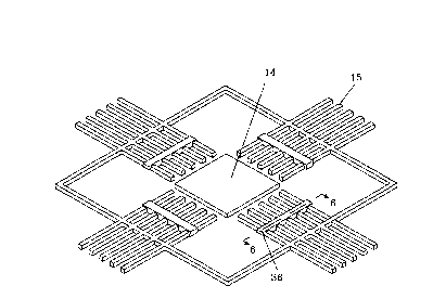
| (54) Titre français: | MATERIAU DE STABILISATION ET D'ESPACEMENT POUR DISPOSITIF A SEMICONDUCTEUR |
| (54) Titre anglais: | STABILIZER/SPACER FOR SEMICONDUCTOR DEVICE |
| Statut: | Réputée abandonnée et au-delà du délai pour le rétablissement - en attente de la réponse à l’avis de communication rejetée |
| (51) Classification internationale des brevets (CIB): |
|
|---|---|
| (72) Inventeurs : |
|
| (73) Titulaires : |
|
| (71) Demandeurs : |
|
| (74) Agent: | KIRBY EADES GALE BAKER |
| (74) Co-agent: | |
| (45) Délivré: | |
| (22) Date de dépôt: | 1992-12-30 |
| (41) Mise à la disponibilité du public: | 1993-07-08 |
| Licence disponible: | S.O. |
| Cédé au domaine public: | S.O. |
| (25) Langue des documents déposés: | Anglais |
| Traité de coopération en matière de brevets (PCT): | Non |
|---|
| (30) Données de priorité de la demande: | ||||||
|---|---|---|---|---|---|---|
|
Note : Les revendications sont présentées dans la langue officielle dans laquelle elles ont été soumises.
Note : Les descriptions sont présentées dans la langue officielle dans laquelle elles ont été soumises.
2024-08-01 : Dans le cadre de la transition vers les Brevets de nouvelle génération (BNG), la base de données sur les brevets canadiens (BDBC) contient désormais un Historique d'événement plus détaillé, qui reproduit le Journal des événements de notre nouvelle solution interne.
Veuillez noter que les événements débutant par « Inactive : » se réfèrent à des événements qui ne sont plus utilisés dans notre nouvelle solution interne.
Pour une meilleure compréhension de l'état de la demande ou brevet qui figure sur cette page, la rubrique Mise en garde , et les descriptions de Brevet , Historique d'événement , Taxes périodiques et Historique des paiements devraient être consultées.
| Description | Date |
|---|---|
| Réputée abandonnée - omission de répondre à un avis sur les taxes pour le maintien en état | 2001-01-02 |
| Inactive : Morte - RE jamais faite | 2001-01-02 |
| Demande non rétablie avant l'échéance | 2001-01-02 |
| Inactive : Abandon.-RE+surtaxe impayées-Corr envoyée | 1999-12-30 |
| Demande publiée (accessible au public) | 1993-07-08 |
| Date d'abandonnement | Raison | Date de rétablissement |
|---|---|---|
| 2001-01-02 |
Le dernier paiement a été reçu le 1999-05-25
Avis : Si le paiement en totalité n'a pas été reçu au plus tard à la date indiquée, une taxe supplémentaire peut être imposée, soit une des taxes suivantes :
Les taxes sur les brevets sont ajustées au 1er janvier de chaque année. Les montants ci-dessus sont les montants actuels s'ils sont reçus au plus tard le 31 décembre de l'année en cours.
Veuillez vous référer à la page web des
taxes sur les brevets
de l'OPIC pour voir tous les montants actuels des taxes.
| Type de taxes | Anniversaire | Échéance | Date payée |
|---|---|---|---|
| TM (demande, 5e anniv.) - générale | 05 | 1997-12-30 | 1997-05-28 |
| TM (demande, 6e anniv.) - générale | 06 | 1998-12-30 | 1998-06-24 |
| TM (demande, 7e anniv.) - générale | 07 | 1999-12-30 | 1999-05-25 |
Les titulaires actuels et antérieures au dossier sont affichés en ordre alphabétique.
| Titulaires actuels au dossier |
|---|
| TEXAS INSTRUMENTS INCORPORATED |
| Titulaires antérieures au dossier |
|---|
| DONALD C. ABBOTT |

