Note : Les descriptions sont présentées dans la langue officielle dans laquelle elles ont été soumises.
CA 02091332 2000-09-18
20104-8778
1
SEMICONDUCTOR NON-VOLATILE MEMORY WITH TUNNEL OXIDE
The invention relates to a method of manufacturing a semiconductor
device whereby a semiconductor body is provided at a surface with a non-
volatile
memory element in the form of a MOS transistor with floating gate electrode,
which
transistor is separated from a subjacent surface region of the semiconductor
body by
silicon-enriched tunnel oxide. The invention also relates to a semiconductor
device
manufactured by such a method.
Such a method is known from, for example, US-A-4,849,248.
MOS transistors with floating gate electrodes form the memory elements
in many non-volatile memories known under the names EEPROM, EPROM, flash-
EEPROM, flash-EPROM, etc. In all these types of memories, the written
information is
formed by the charge state of the floating gate electrode, and thus by the
threshold
voltage of the MOS transistor. Readout takes place by, for example, a control
gate
which usually lies above the floating gate, which is electrically insulated
therefrom, and
to which such a voltage can be applied during readout that the transistor
becomes or
does not become conducting, depending on the information stored.
Tunnelling of electrons from or to the floating gate electrode through the
tunnel oxide is often used for charging or discharging of the floating gate
electrode. To
obtain a suitable tunnelling current, very thin tunnel oxide layers are
required in
conventional memories of the order of, for example, 8-10 nm. A number of
disadvantages, however, are inherent in such thin layers. The thin tunnel
oxide must be
provided together with oxide layers of greater thickness which form gate
oxides of the
memory transistors and possibly of other MOS transistors. During manufacture
it is
practically always necessary to provide photoresist on the gate oxide already
formed for
the purpose of photolithographic operations, which may adversely affect the
quality of
the gate oxide. As to the operation of the device, the thin tunnel oxide has
the effect
PHIeT 14.006 2 05.06.1992
that the capacitance between the floating gate electrode and surface zones in
the
semiconductor body is increased. These zones comprise, for examp:(e, portions
of the
semiconductor body adjacent the drain zone in the case of an EEPROM
(Electrically
Erasable PROM) and the source and drain zones in the case of, for example, a
flash-
y EEPROM or flash-EPROM (Electrically Programmable ROM). Owing to this
parasitic
capacitance, the capacitance ratios between the floating gate and the control
gate and
between the floating gate and the semiconductor body become such that
comparatively
high voltages must be applied to the control gate for achieving the tunnelling
effect.
These high voltages may cause problems in the drive electronics and/or in the
logic
circuits in the case of a so-called embedded memory. It is often desirable,
accordingly,
to reinforce the tunnelling effect in the sense that the tunnelling current is
sufficiently
strong also at lower voltages. It should be ensured in this case, however,
that the
retention time of the memory is sufficiently long, 1. e. that the information
stored at the
floating gate is maintained for a sufficient period and does not prematurely
disappear
owing to leakage of electric charge. It is often found in practice that
reinforcement of
the tunnelling effect is accompanied by an increase in leakage currents.
Fig. 13 of the cited US Patent 4,849,248 shows a device of the kind
mentioned in the opening paragraph in which the tunnelling effect is
reinforced in that
the silicon content in the tunnel oxide is increased through irriplantation of
silicon ions
into the tunnel oxide. 'When the usual techniques are used, this known device
also
requires photoresist layers, both for defining the tunnel oxide and for local
implantation
of the silicon ions. In addition, a tunnel oxide is formed which is
considerably thinner
than the adjacent gate oxide, also in this known process.
The invention has for its object inter alia to provide a method of the kind
mentioned in the opening paragraph whereby the tunnelling effect is reinforced
without
the retention time reaching an unacceptably low value. The invention also has
for its
object to indicate a simple method whereby the direct application of a
photoresist layer
on the gate oxide is avoided. A further object of the invention is to provide
an
EEPROM oz EPROM memory based on the tunnelling effect in which the thickness
of
the tunnel oxide corresponds to the thickness of the usual gate oxides, while
excessively
PHN 14.006 3 05.06.1992
high voltages at the control gate are avoided.
According to the invention, a method of the kind mentioned in the
opening paragraph is characterized in that the tunnel oxide is enriched with
silicon in
that a silicon layer is deposited on the tunnel oxide and subsequently
comparatively
heavy ions are implanted into the silicon layer with such an energy that, at
the given
thickness of the silicon layer, silicon atoms are driven from the silicon
layer into the
tunnel oxide by the ion implantation.
It was found that a memory manufactured by the method described here
has a satisfactory operation. The method according to the invention is very
simple.
After growing of the gate oxide, a khin layer of polycrystalline silicon is
deposited,
referred to hereinafter as poly or poly layer for short.
On this layer, a photoresist mask may subsequently provided, defining the
tunnel oxide and separated from the gate oxide by the poly layer. The
tunnelling current
in the gate oxide is increased through implantation of heavy ions, such as As,
after
which the photoresist mask is removed again.
In special cases, it may be advantageous to make the tunnel oxide thinner than
the gate
oxide. An embodiment which has the advantage inter alga that the capacitive
coupling
between the floating gate and the substrate is improved, is characterized in
that a gate
oxide of the same or at least substantially the same thickness as the tunnel
oxide is
provided between the floating gate electrode and a channel region of the MOS
transistor. In this embodiment, it is in addition not necessary to carry out a
separate
oxidation step for providing the tunnel oxide, but the tunnel oxide can be
formed
simultaneously with the gate oxide. An embodiment in which the gate
oxide/tunnel
oxide is exposed to as few treatments as possible which could impair the
quality of the
oxide is characterized in that the floating gate electrode is formed at least
partly from
the silicon layer.
On the one hand, the thickness of the silicon layer must not be too small,
to prevent the implanted ions being shot clean through the layer; on the other
hand, the
layer must not be too thick either, because it is difficult for the excited
silicon atoms to
reach the tunnel oxide in the case of a too great thickness. Experiments have
shown that
favourable values for the thickness of the silicon layer lie between 25 nm and
200 nm.
Preferably, the thickness is at least approximately 100 nm.
PHN 14.006 4 05.06.1992
Specific values for the energy with which the ions are implanted into the
silicon layer,
depending inter alia on the thickness of the silicon layer and on the type of
ions, lie in
the range between approximately 50 Ke'V and 150 KeV. Preferably the
implantation
energy is at least approximately 80 KeV.
After the step involving implantation, the floating gate electrode may
advantageously be defined from the silicon layer if the silicon layer is
sufficiently thick
in view of, for example, the resistance of the layer. An embodiment which is
important
especially for thinner silicon layers is characterized in that a
polycrystalline silicon layer
is deposited on the silicon layer after the implantation step, after which the
floating gate
electrode is defined from the combined layer. If the silicon layer is
sufficiently thick for
forming the floating gate, this layer may be doped with, for example, P before
or after
the implantation with heavy ions. If the silicon layer is too thin for the
floating gate, it
is preferably not doped until after the additional poly deposition.
The invention will be explained in more detail with reference to a few
embodiments and the accompanying diagrammatic drawing in which:
Fig. 1 is a cross-section of a semiconductor device manufactured by a
method according to the invention;
Figs. 2-5 show the device of Fig. 1 in a number of stages of manufacture;
Figs. 6-11 show a second embodiment of a method according to the
invention;
Figs. 12-14 show a third embodiment of a method according to the
invention;
Figs. 15-18 show a fourth embodiment of a method according to the
invention; and
Fig, 19 is a cross-section of a further embodiment of a semiconductor
device manufactured by means of a method according to the invention.
It is noted that the Figures are diagrammatic and not drawn to scale.
Corresponding components in the various embodiments are usually given the same
PHN 14.006 5 05.06.1992
reference numerals. Semiconductor regions of the same conductivity type are
generally
hatched in the same direction.
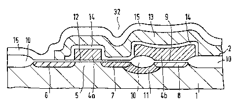
Fig. 1 shows a semiconductor device with a semiconductor body 1 of
silicon. Obviously, any other suitable semiconductor material may be used
instead of
silicon. The body 1 is provided at its surface 2 with a non-volatile memory
element 3 in
the form of an MOS transistor with floating gate electrode 4. Two portions 4a
and 4b of
the gate 4 are shown in the drawing, which portions are interconnected outside
the
plane of the drawing. It is noted that, although the letters M and O in the
acronym
MOS denote metal and oxide, respectively, the invention is not limited to this
type of
transistor, and that embodiments in which the gate electrode is made from a
material
other than metal, for example, of doped semiconductor material such as
polycrystalline
silicon, and/or in which the gate dielectric is not made of an oxide but of
another
material or of a combination of different materials, should also be regarded
as covered
by the term MOS transistor. The information is stored in the form of electric
charge on
the floating gate electrode 4 and determines the threshold voltage of the
transistor. The
gate electrode 4 is completely surrounded by dielectric material, so that the
charge
cannot flow away and the element obtains its non-volatile properties. The
portion 4a of
the floating gate lies over the channel 5 between the source 6 and the drain 7
of the
transistor. The portion 4b of the floating gate lies over a surface region 8,
also called
tunnel xegion hereinafter, which is separated from the gate electrode 4 by the
interposed
tunnel oxide 9. At certain voltages between the gate 4 and the tunnel region
8, electrons
can tunnel from the gate 4 to the region 8 or from the region 8 to the gate 4
through the
tunnel oxide for adjusting the charge state of the gate 4. To increase the
tunnelling
effect, the tunnel oxide 9 is enriched with silicon, i. e. the silicon content
in the layer 9
2S is higher than in the case of a stoichiometric composition of the layer 9.
Thanks to this
reinforced tunnelling effect, a sufficiently strong tunnelling current can be
obtained also
with a tunnel oxide of a greater thickness than usual, at comparatively low
voltages. As
a result of this the tunnel oxide may be provided, for example, with a
thickness such as
is usual for gate oxides of MOS transistors.
~0 In this embodiment the semiconductor body 1, or at least a layer-shaped
portion thereof adjoining the surface, is of the p-type. The transistor 3 is
provided in an
active region which is bounded by the comparatively thick field oxide 10. The
transistor
~1
PHN 14.006 6 05.06.1992
3 of the n-channel type comprises n-type source/drain zones 5 and 7. The
channel
region 8 lies outside the transistor region in this embodiment and comprises
an n-type
zone 8 which is connected to the drain 7 by the n-type connection zone 11
provided
under the field oxide 10. The tunnel oxide 9 separating the region 8 from the
floating
gate electrode 4 has the same or at least substantially the same thickness as
the gate
oxide 12 above the channel region of the transistor. The floating gate
electrode 4 is of
n-type doped polycrystalline silicon. Over the floating gate 4, a control
electrode or
control gate 13 is provided, which is also of n-type polycrystalline silicon.
The poly
layers 4 and 13 are separated by the interpoly dielectric 14 made of oxide,
but which
may alternatively be made of, for example, nitride or a combination of oxide
and
nitride. The thickness of the layer 14 is chosen so that the capacitive
coupling between
the gates 4 and 13 compared with the capacitive coupling between the gate 4
and the
semiconductor body is as great as possible, because in that case the potential
of the
floating gate 4 can be most easily adjusted, i.e. i.e. with the smallest
possible voltages
at the control gate 13, far example, during writing or erasing. The thickness
of the
layer 14 is chosen to be not too great and the thickness of the oxide layers 9
and 12 is
chosen to be not too small for this reason. Specific values for the thickness
of the oxide
layers 9/12 lie in the 12-40 nm range, for example 25 nm, and approximately 25
nm
(effective oxide thickness) for the interpoly layer 14. The device is covered
with a thick
oxide layer 15 in which openings (not shown in the drawing) for contacts can
be
formed.
The device described here may be constructed as an EEPROM, in which
case the transistor 3 is coupled through the drain to a selection transistor
(not shown),
whose gate is connected to a word line.
The manufacture of the device starts with a p-type silicon substrate 1 of a
usual resistivity. The body 1 is first provided at the surface with a heavily
doped n+
zone, preferably doped with As, at the area of the connection zone 11 to be
formed
and, if necessary, with p-type channel stopper zones at the area of the field
oxide 10 to
be provided outside the region of the zone 11. These channel stoppers are not
shown in
the drawing. Then the field oxide 10 is provided in usual manner, whereby the
connection zone 11 is obtained below the portion of the field oxide situated
in the centre
of the drawing. Then the n-type zone 8 can be formed in the tunnel region by a
PI3N 14.006 7 05.06.1992
phosphorus implantation. In view of the quality of the tunnel oxide to be
grown over the
zone 8, the doping concentration of the zone 8 is chosen to be comparakively
low, for
example, 1 to 2.10'a atoms/cm3. Any masking layers present on the surface can
then be
removed, after which the gate oxide 12 and the tunnel oxide 9 are
simultaneously
formed by thermal oxidation. The device is then in the stage shown in Fig. 2.
An amorphous or polycrystalline thin silicon layer 16 is deposited on the
configuration thus obtained, see Fig. 3. The thickness of the silicon layer is
approximately 100 nm. On the silicon layer 16, a photoresist layer is provided
from
which a doping mask 17 with an opening 18 at the area of the tunnel region 8
is
formed. It is noted that the mask 17 is separated from the gate oxide 12 and
the tunnel
oxide 9 by the interposed silicon layer 16, so that it cannot or substantially
not influence
the quality of these oxide layers, as is often the case when photoresist is
provided
directly on oxide. The silicon layer 16 is subsequently subjected to an
implantation
treatment with comparatively heavy ions, compared with silicon, through the
opening
18. The dopant for this implantation may be selected from several elements,
for
example, As, Sb, Ge, etc. In the present example, As is chosen which is
implanted into
the silicon layer 16 at an energy of between 50 KeV and 150 KeV, in particular
at an
energy of approximately 80 KeV. The implantation intensity is approximately 1
to
3.10'5 atoms per cm2. The implantation energy and the thickness of the silicon
layer 16
are such that the As+ ions are implanted into the silicon layer at least for
the major part
and that at most a negligible fraction ends up in the tunnel oxide and
possibly in the
substrate 1. During the implantation, As ions collide with silicon atoms so
that, given
the small thickness of the layer 16, silicon of the layer 16 is propelled into
the tunnel
oxide 9, thus forming a silicon-enriched region there. After the implantation,
the
photoresist mask 17 is removed and, if so desired, the silicon layer may be
made
thicken up to, for example, 500 nm. The silicon layer 19 thus obtained (Fig.
4) is then
doped with, for example, P. In a next step, a photoresist mask 20 is formed
which
defines the floating gate 4, after which the unmasked portions of the silicon
layer 19 are
removed by, for example, reactive ion etching. The portions 4a and 4b have now
been
formed, as is shown in Fig. 5.
The n-type source/drain zones 6 and 7 are then formed. 'The device may
be further finished by usual steps riot shown in the drawing. First the mask
20 may be
PHN 14.006 8 05.06.1992
removed, after which the interpoly dielectric is provided, for example,
through
deposition from the gas phase. If the layer 14 is made of silicon oxide, the
interpoly
dielectric may obviously also be obtained through oxidation of the poly. After
patterning
of the layer 14, a second doped polycrystalline silicon layer is provided,
from which the
control gate 13 is formed. A glass layer 15 is provided ovex the entire
assembly through
deposition from the gas phase, which layer is provided with contact windows in
usual
manner, for example (outside the plane of the drawing), with the source 6
and/or drain
7 and/or with the control gate 13. After this the wiring may be formed in a
single-layer
or multilayer metallization in usual manner.
The memory cell described here may be operated at voltages which are
comparable to the voltages usual for non-volatile memory elements having a
very thin
tunnel oxide (8 nm or less), with comparable values for the tunnelling
current. Thus,
for example, the tunnelling current was approximately 10 nA at a voltage of 10
V
between the floating gate 4 and the tunnel region 8 in a practical embodiment.
The
capacitive coupling between the floating gate 4 and the substrate 1 is reduced
by the
comparatively thick tunnel oxide, which offers advantages for the operation of
the
device. Since the tunnel oxide can be formed simultaneously with the normal
gate
oxide, the manufacture of the device is considerably simplified. It should
furthermore
be noted in particular that the photoresist layers required in the various
stages are not
provided directly on the gate oxide 12 or the tunnel oxide 9 in the process
described
here; so that they cannot or practically not impair the quality of the
subjacent oxide.
Figs. 6-11 are cross-sections of a semiconductor device manufactured
according to a second embodiment of a method according to the invention, in
various
stages of the process. The device, which in this case may form part of a flash-
2S EEPROM, again comprises a p-type silicon substrate 1 in which active
regions are
defined at the surface by the field oxide 10. A gate oxide layer 25 of the
same thickness
as the oxide layer 12 in the preceding embodiment is provided on the surface
of the
active region. Then a comparatively thin polycrystalline silicon layer 16 is
again
deposited over the entire surface, Fig. 6. In a next step, see Fig. 7, a
photoresist mask
26 is provided on the silicon layer 16 for the implantation which reinforces
the
tunnelling effect. Although this implantation need only be carried out over
part of the
active region, the mask 26 in the embodiment shown here leaves the entire
active region
PHN 14.006 9 05.06.1992
exposed. Tt is tme that portions of the gate oxide next to the tuW elling
oxide to be
formed are enriched with silicon thereby, but this does not pose a problem
because
these portions of the gate oxide can be removed in a next step. In some cases
the mask
26 may be entirely omitted, so that the silicon layer 16 is exposed to the
implantation
over its entire surface. Often, however, it is desirable to mask the surface
locally, for
example; in 'view of the transistors in the peripheral circuits. After the
mask 26 has
been provided, the treatment reinforcing the tunnelling effect is carried out
again in the
same manner as in the preceding embodiment, through implantation of, for
example, As
ions into the silicon layer 16 at such an energy that silicon atoms are
implanted into the
gate oxide 25 as a result of this implantation. The gate oxide 25 is
accordingly enriched
with silicon over the entire active region shown in the drawing. After the
implantation,
the mask 26 is removed and the silicon layer may be made thicker, if so
desired, and
may be doped with P or some other suitable impurity. When the silicon layer 16
has the
desired thickness and resistivity, the floating gate electrode may be defined
by means of
the photaresist mask 27 (Fig. 8). The floating gate electrode 4 is obtained by
removal
of the non-masked polycrystalline material (Fig. 9). The n-type source and
drain zones
6 and 7 are formed by, for example, implantation of As-ions and a heat
treatment (Fig.
10). The photoresist mask 27 may then be removed. Then the interpoly
dielectric 14
may be provided by deposition, followed by the deposition of a second poly
layer.
These layers are patterned in usual manner (Fig: 11) to obtain the control
gate 13 which
overlaps the floating gate 4. The portion of the gate oxide 25 not covered by
the
floating gate 4 is also removed. The oxide with reinforced tunnelling effect,
accordingly, is limited entirely to the portion situated below the gate 4. The
process
may be continued in usual manner with the application of a glass layer over
the entire
assembly, etching of contact windows therein, and the provision of the
metallizatian.
The device described here may be used in a so-called flash-EEPROM, in
which electrons tunnel from the substrate (or source or drain) to the floating
gate or
from the floating gate to the substrate (or source ar drain) during writing
and erasing.
Obviously, the device may also be operated as an EEPROM when a selection
transistor
is connected in series with the floating gate transistor.
As can be seen in Fig. 1l; the control gate 13 overlaps the floating gate
4. A configuration in which this overlap does not occur and which as a result
can be
PI-IN 14.006 10 05.06.1992
smaller and thus particularly suitable for being integrated with other
elements into a
large memory is known under the designation "stacked EEPROM". A method
according
to the invention for the manufacture of a stacked EEPROM is described in the
next
embodiment with reference to Figs. 12-14, which in cross-section show a memory
element in various stages of manufacture. Manufacture runs in an analogous
manner
compared with the process described in the preceding example up to and
including the
stage depicted in Fig. 7, where the oxide layer 25 is enriched with silicon
through
implantation with heavy ions, for example, As ions, into the silicon layer 16.
By a
method which is known per se, a pattern of lanes can be formed from the
silicon layer
16 by means of a photoresist mask, after which the photoresist mask is removed
again.
Such a lane is shown in the plane of the drawing in the cross-suction of Fig.
12. Then
the interpoly dielectric layer 14 and the second poly layer 13 are provided.
After this
the photoresist mask 29 is formed, Fig. 12, defining the gate configuration.
The layers
13, 14 and 16 are etched one after the other, so that the stack shown in Fig.
13 is
1 S obtained with the floating gate 4, the interpoly dielectric 14, and the
control gate 13.
The control gate 13 does not overlap the floating gate 4 any more (at least in
the plane
of the drawing) so that a somewhat more compact structure than in the
preceding
embodiment is obtained. In a next step, the source and drain zones 6 and 7 are
formed
through implantation of As and the phatoresist mask 29 is removed again. In a
next
step, shown in Fig. i4, the flanks of the poly stack are covered with an
insulating layer
30, for example, in the form of so-called spacers. These may be provided in
known
manner, for example, through oxidation of the sides of the stack and/or
anisotropic
etching back of a layer of oxide or another suitable insulating material which
was
deposited over the entire assembly. During this, the tunnel oxide not covered
by the
floating gate may be simultaneously removed to obtain contact windows, so that
the
tunnel oxide is strictly limited to the channel region of the transistor.
With the next embodiment, a method according to the invention is
described for manufacturing a flash-EPROM in which charge is applied to the
floating
gate through injection of hot electrons from the substrate and in which on the
other
hand electrons can tunnel from the floating gate to the substrate. Fig. 15
shows in
cross-section the device in the stage where, after growing of the gate oxide
25 and the
thin poly layer 16, the photoresist mask 32 is provided on the surface. The
photoresist
PHN 14.006 11 05.06.1992
mask 32 masks a substantial portion of the active region, at least a portion
of the
channel of the transistor to be formed. The implantation with high-energy
heavy ions,
for example, As ions, as described above is carried out through the opening 33
in the
mask 32 for enriching the gate oxide 25 With silicon to reinforce the
tunnelling effect.
Since the enrichment is only local in this example, the enriched region in
Figs. 16-18 is
marked with a broken line in the gate oxide 25. After the As implantation, the
polylayer
16 is made thicker, if so desired, and doped with, for example, P, after which
the mask
34 is provided over the floating gate to be formed (Fig. 16). The floating
gate 4, see
Fig. 17, is then formed from the polylayer 16 by etching, after which the
source and
drain zones 6 and 7 are formed through implantation of As ions into the
substrate 1. In
a next stage, the interpoly dielectric and the second poly layer are
deposited, after
which the stn~eture shown in Fig. 18 is obtained through etching. The device
may be
further completed with the usual steps.
The control gate 13 overlaps the floating gate 4 on either side. The
silicon-enriched tunnel oxide 35 represents only a portion of the gate oxide
25, in Lhis
example a portion adjoining the source zone 6. During writing, hot electrons
can be
injected onto the floating gate 4 through the gate oxide 25 near the drain 7.
During
erasing; this charge can tunnel to the source zone 6 through the tunnel oxide
35.
Fig. 19 is a cross-section of a modification of the structure shown in Fig.
18, in which the floating gate 4, the interpoly dielectric 14, and the control
gate 13 are
provided as a stack. The tunnel oxide 35 is again situated near the source
zone 6,
similar to the preceding embodiment. The manufacturing process for the device
is
largely identical to the method described above, obviously with the exception
of the
mask 34 defining the gate, which is not provided until after the deposition of
the second
poly layer.
It will be obvious that the invention is not limited to the embodiments given
here, but
that many modifications are possible to those skilled in the art. Thus other
heavy ions
may be used for enriching the tunnel oxide with silicon instead of As ions,
such as, for
example, Sb, Ge, Si and Kr.