Note : Les descriptions sont présentées dans la langue officielle dans laquelle elles ont été soumises.
CA 02092610 1998-03-18
TRANSMITTING AND RECEIVING SYSTEM IN BASE STATION
The present invention relates to a transmitting and receiving
system in a base station for a digital mobile telephone system adopting a time-
division multiple-access system (TDMA) and, more particularly, to a
transmission/reception data processing circuit which permits ready transition
from a full- to a half-rate system without alteration of any hardware and with
mere simple alteration of firmware.
By the term "half-rate system" is meant a mobile telephone system
for speech communication at one-half the information transmission rate of the
full-rate system. According to this half-rate system, about double the capacity
of speech communication is permitted over the full-rate system. By way of
example, in the Japanese standard digital mobile telephone system, one frame
is 40 milliseconds and is divided-in-time into 6 slots. In the full-rate system, two
slots in one frame are used for communication, while in the half-rate system a
single slot in the frame is used for communication.
Figure 3 shows a prior art time-division multiple-access-system
transmission/reception data processing circuit of this type. As shown, the circuit
has independent data processing means 126, 128 and 130 and 2-port RAMs
127, 129 and 131 for individual channels, and also has multiplexing/separating
means 125 for multiplexing and separating data of individual channels. The
means 125 is provided between the data processing means 126, 128 and 130
and a radio transmitting/receiving circuit 11.
Such a prior art circuit has a transmission/reception data
processing unit and a 2-port RAM for each channel. When the number of
channels to be multiplexed is changed such as in the case of transition from thefull-rate system to the half-rate system, it is required to add and alter the
hardware with the resultant cost.
For example, the Japanese standard digital mobile telephone
system prescribes the full-rate system of 3-channel multiplexing to be in
practical use for the first time, and the half-rate system of 6-channel multiplexing
.~
,
CA 02092610 1998-03-18
~, _
to be introduced about two years afterwards. It is also allowed that the full- and
half-rate systems coexist at a single radio frequency. Therefore, if processing
units for the 3 channels necessary for the initial full-rate system are provided in
the prior art structure where a data processing unit is provided for each channel,
5 it becomes necessary to replace the transmission/reception data processing
units at the time of the future introduction of the half-rate system. On the other
hand, providing data processing units for 6 channels to cope with the half-rate
system from the outset causes a great initial investment and resultant increasedcost.
In the half-rate system the bit rate is one-half the bit rate in the full-
rate system, so that about one-half the transmission/reception data processing
capacity suffices. Therefore, to be compatible with both the half- and full-ratesystems it is necessary to have data processing units having the full-rate system
processing capacity for about 6 channels, also resulting in increased cost.
An object of the invention is therefore to provide a transmitting and
receiving system in a base station, the system being capable of permitting the
transition from a full-rate system to a half-rate system to be readily realized
without hardware alteration and merely with a simple alteration of firmware.
In the preferred aspect of the present invention, the
20 transmission/reception data processing circuit executes disassembling and
assembling of control signals to and from a plurality of slots for all channels to
be multiplexed to a single radio frequency, and also executes data processing
for each slot on control signals for all channels to be multiplexed to a single
radio frequency. It further executes data processing for each slot on speech
25 signals of all channels to be multiplexed to a single radio frequency. It is thus
possible to readily realize the transition from the full-rate system to the half-rate
system without hardware alteration and merely with a simple firmware alteration.The invention is a transmitting and receiving system in a base
station in a time-division multiple-access digital mobile telephone system, and
30 has a control signal inpuVoutput unit for inputting and outputting control signals
from and to an external system, a speech signal inpuVoutput unit for inputting
CA 02092610 1998-03-18
.."_,~
and outputting speech signals from and to the external system, a plurality of
transmitting/receiving units, a control signal bus connecting the control signalinpuVoutput unit and the plurality of transmitting/receiving units, and a speechsignal bus connecting the speech signal inpuVoutput unit and the plurality of
5 transmitting/receiving units. The plurality of transmitting/receiving units each
includes a radio transmitting/receiving circuit and a transmission/reception data
processing circuit. Each of the transmission/reception data processing circuits
includes first and second data processing means, and first and second 2-port
RAMs. The first data processing means assembles and disassembles control
10 signals to and from a plurality of slots for all channels to be multiplexed. The
first 2-port RAM is connected to the first data processing means and also to thecontrol signal bus. The second data processing means executes, for each slot,
data processing on control signals for all channels to be multiplexed to a single
radio frequency. The second 2-port RAM is connected to both the first and
15 second data processing means. The first data processing means may be a
universal microprocessor, and the second data processing means may be a
high-speed single-chip microprocessor.
The aforementioned transmitting and receiving system of the
invention operates as follows. In response to a down-coming control signal
20 transmitted from the external system, the control signal writes into the first 2-
port RAM. The first data processing means adds an address field and a control
field to the control signal, and in the case of an octet number which cannot be
transmitted by one unit, adds a bit for signal disassembling and assembling after
the division into a plurality of units, and writes a resulting signal into the second
25 2-port RAM. When the control signal has been written into the 2-port RAM, the second data processing means forms a predetermined down-coming format,
transmits resulting data in an assigned slot, and executes scrambling and secretprocessing on the speech signal input from the external system. In response
to an up-going control signal the second data processing means takes out the
30 control signal portion and executes de-interleaving, FEC coding and CRC
checking on the taken-out speech signal. When a reception slot is assigned to
CA 02092610 1998-03-18
-
a physical channel for communication, the second data processing means takes
out the speech signal portion and executes scrambling and secret processing
on the taken-out speech signal.
Other objects and features will be clarified from the following
5 description with reference to the attached drawings, in which:
Figure 1 is a block diagram showing a transmission/reception data
processing circuit according to an embodiment of the present invention;
Figure 2 is a block diagram showing an embodiment of the
transmitting and receiving system in a base station according to the present
1 0 invention;
Figure 3 is a block diagram showing a prior art
transmission/reception data processing circuit;
Figure 4 is a time chart showing a frame configuration of a TDMA
signal;
Figure 5 is a time chart showing the signal format of one unit of a
physical channel for control;
Figure 6 is a time chart showing the signal format of one unit of a
physical channel for communication;
Figure 7 is a view showing data processing for an upgoing first unit
of a physical channel for control;
Figure 8 is a view showing data processing for FACCH of a
physical channel for communication; and,
Figure 9 is a view showing disassembling and assembling for
plural units for a control signal.
An embodiment of the present invention will now be described with
reference to the drawings. Figure 2 is a block diagram showing the transmitting
and receiving system in a base station of a digital mobile telephone system
utilizing a time-division multiple-access system according to the invention.
The transmitting and receiving system in the base station
comprises a control signal inpuVoutput unit 20 for inputting and outputting
control signals from and to an external system, a speech signal inpuVoutput unit
CA 02092610 1998-03-18
.~",~
30 for inputting and outputting speech signals from and to the external system,
a plurality of transmittingtreceiving units 10a to 10c including respective radio
transmitting/receiving circuits 11 a to 11 c and transmission/reception data
processing circuits 12a to 12c, a control signal bus 40 connecting the control
signal inpuVoutput unit 20 and the transmitting/receiving units 10a to 10c, and
a speech signal bus 40 connecting the speech signal inpuVoutput unit 30 and
the transmitting/receiving units 10a to 10c. The control signal inpuVoutput unit20 communicates with the external system in accordance with CCITT X. 25
protocol for data transmission between the external system and each of the
transmitting/receiving units 10a to 10c. The speech signal inpuVoutput unit 30
has functions for serving as an interface for the external system of, for instance,
2,048-kbps MD codes and TTL-level signals in the speech signal bus 50, and
also for extracting and adding an 8-kHz synchronous signal. The
transmitting/receiving units 10a to 10c transmit and receive the control or
speech signals to and from the mobile telephone sets using radio frequency
signals. The transmitting/receiving units 10a to 10c comprise respective radio
transmitting/receiving circuits 11 a to 11 c and transmission/reception data
processing circuits 12a to 12c. The radio transmitting/receiving circuits 11a to11c transmit and receive triplexed or hexaplexed 42-kbps data to and from the
mobile telephone sets by using radio frequency signals based upon a n/4-shift
QPSK system. The transmission/reception data processing circuits 12a to 12c
execute processing of first and second layers of the control signal, scrambling
of the speech signal, etc., in each of the multiplexed channels.
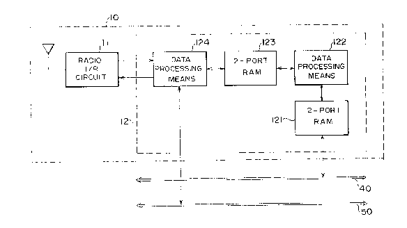
Figure 1 is a block diagram showing the transmitting/receiving unit
according to this embodiment. The transmitting/receiving unit 10 includes the
radio transmitting/receiving circuit 11 and the transmission/reception data
processing circuit 12. The transmission/reception data processing circuit 12
includes a first 2-port RAM 121, first data processing means 122, a second 2-
port RAM 123 and second data processing means 124. The first 2-port RAM
121 and the second data processing means 124 are connected to the control
and speech signal buses 40 and 50, respectively. The first data processing
CA 02092610 1998-03-18
.",_
means 122 may be realized with peripheral circuits of a universal
microprocessor (hereinafter referred to as a MPU), such as memories, address
decoders and timers. The second data processing means 124 may be realized
with, for instance, a high-rate single-chip MPU or a single-chip digital signal
5 processor (hereinafter referred to as a DSP). The first 2-port RAM 121, which
has a plurality of control signal buffers for the rate-matching of the control signal
inpuVoutput unit, has a capacity of several 10 kB (kilo Bytes). The second 2-
port RAM 123 has a buffer for one slot for each channel, and thus its capacity
is several 100 B to several kB.
More specifically, the embodiment, as shown in Figures 1 and 2,
comprises a control signal inpuVoutput unit 20 for inputting and outputting
control signals from and to the external system, a speech signal inpuVoutput
unit 30 for inputting and outputting speech signals from and to the external
system, a plurality of transmitting/receiving units 10a to 10c each including a
15 radio transmitting/receiving circuit 11 and a transmission/reception data
processing circuit 12, a control signal bus 40 connecting the control signal
inpuVoutput unit 20 and the plurality of the transmitting/receiving units 10a to10c, and a speech signal bus 50 connecting the speech signal inpuVoutput unit
30 and the plurality of the transmitting/receiving units 10a to 10c. The
20 transmission/reception data processing circuit 12, as it features means of the
embodiment, comprises first data processing means 122 for disassembling and
assembling into and from a plurality of slots control signals for all channels to
be multiplexed to a single radio frequency, a first 2-port RAM 121 connected to
the first data processing means 122 and also to the control signal bus 40,
25 second data processing means 124 for executing data processing for each slot
on the control signals for all channels to be multiplexed to a single radio
frequency and also executing for each slot data processing on the speech
signals for all channels to be multiplexed to a single radio frequency, and a
second 2-port RAM 123 connected to the first data processing means 122 and
30 also to the second data processing means 124.
CA 02092610 1998-03-18
-
Next, single formats and contents of the data processing will be
described by taking the Japanese standard digital mobile telephone system as
an example. The standards of the Japanese standard digital mobile telephone
system are published as RCR STD-27 by the Research & Development Center
5 for Radio Systems.
Figure 4 shows the format of a time-divisional-multiplexed signal
transmitted as a radio signal. In Figure 4, slots in a frame are labeled ST#0 toST#5. One superframe comprises 18 frames each comprising six slots. Each
slot can be assigned as an independent channel (physical channel). In the case
10 of a physical channel for control (control physical channel) or a physical channel
for communication (communication physical channel) for the full-rate system,
however, two slots in one frame are used. That is, channels ST#0 and ST#3,
ST#1 and ST#4, or ST#2 and ST#5 are assigned to the single physical channel.
For the physical channel for the half-rate communication physical channel, a slot
15 in one frame is used. Thus, three to six physical channels are multiplexed for
each radio frequency.
Figures 5 and 6 show signal formats in one slot of the control and
communication physical channels. In Figure 5, there are C and R guard times
for the burst transient response, P preambles, SW synchronous words, CC color
20 codes, CAC control signals (PCH, BCCH, SCCH), and E collision control bits.
In Figure 6, there are G and R guard times for burst transient response, P
preambles, SW synchronous words, CC color codes, SACCH control channels
covering low rates, FACCH control channels covering high rates, a RCH
housekeeping bit, a SF steal flag, and TCH speech signals. A one-slot signal
25 is obtained by adding the preamble P, the synchronous word SW, the color
code CC, etc., to the speech signal.
Figures 7 and 8 show the flow of one unit of signal data processing
for control and a high-rate coverage control channel as respective examples.
In Figure 7, W is a bit for signal disassembling and assembling, and 00 is "Don't
30 care". The high-rate coverage channel is a communication physical channel.
If it is desired to transmit a control signal at a high rate during a communication
CA 02092610 1998-03-18
,,._
session, it is transmitted and received in place of the speech signal data. In the
transmission of a one-unit control signal, CRC encoding, error correction (FEC)
and interleaving are executed. In the reception, converse to the transmission,
de-interleaving, error-correction decoding and a CRC-check are executed.
Figure 9 shows an example of disassembling and assembling
when the control signal is transmitted with a plurality of units. In Figure 9, Wis a bit for signal disassembling and assembling. In the control signal, the bitfor signal disassembling and assembling is added to the head after its division
to a length of an octet number capable of being transmitted by one unit.
Next, the operation of the transmission/reception data processing
circuit according to the embodiment will be described. When a down-coming
control signal is transmitted from the external system, the control signal (layer
3 information) is written into the first 2-port RAM 121 via the control signal
inpuVoutput unit 20 and the control signal bus 40. The first data processing
means 122 adds a layer 2 address field and a control field to the layer 3
information. In the case of an octet number which cannot be transmitted by one
unit, a bit of signal disassembling and assembling is added after the division into
a plurality of units, and the resultant signal is written into the second 2-port RAM
123. Before the data in the second 2-port RAM 123 is taken by the second data
20 ~processing means 124, the data is written successively unit-by-unit into thesecond 2-port RAM 123. When a control signal is written into the second 2-port
RAM 123, the second data processing means 124 executes CRC-coding, FEC-
coding and interleaving as has been described in connection with Figures 7 and
8, adds a preamble, a synchronous signal, a color code, etc. to form the down-
25 coming formats shown in Figures 5(2) and 6(2), and transmits the resultant data
in an assigned slot as shown in Figure 4. When transmissible data has not
been written into the second 2-port RAM 123, the second data processing
means 124 produces idle data. However, the high-rate coverage control
channel is excluded. When a slot is assigned to a physical channel for
30 communication, the second data processing means 124 executes scrambling
and a secret processing on the speech signal input from the external system via
CA 02092610 1998-03-18
"~"",~
the speech signal inpuVoutput unit 30 and the speech signal bus 50, and
transmits the resultant data as the speech signal.
With an up-going control signal, the second data processing means
124 takes out a control signal portion and executes de-interleaving, FEC coding
and a CRC-check, as shown in Figure 7 and 8. If no error is detected by the
CRC-check, it is determined that the data is received, and the reception controlsignal (signal disassembling and assembling bit, layer 2 signal) is written as one
unit into the second 2-port RAM 123. If a reception slot is assigned to a
physical channel for communication, the speech signal portion is taken out, and
then scrambling and secret processing are performed on the taken-out speech
signal. The resultant data is outputted to the speech signal bus 50. The
speech signal is supplied to the external system via the speech signal bus 50
and the speech signal inpuVoutput unit 30.
The second data processing means 124 reads out the data from
the second 2-port RAM 123. If there is received data in the read-out data,
processing means 124 assembles layer 2 information (having been divided into
a plurality of units) by using the bit for signal disassembling and assembling, as
shown in Figure 9. If the received control signal includes layer 3 information,
it is written into the first 2-port RAM 121. The control signal is outputted to the
external system via the control signal bus 40 and the control signal inpuVoutputunit 20.
The first data processing means 122 is operative only when a
control signal is transmitted, and thus it need not be capable of high-rate
processing. Since a plurality of control signals are buffered, processing means
122 is adequately realized with a universal microprocessor of 16 to 32 bits. Thesecond data processing means 124 has to execute processing irrespective of
whether or not there is a control signal, and thus it is required to be capable of
high-rate processing. However, it executes only unit processing, and no large
capacity memory is needed. It is thus adequately realized with a high-rate chip
MPU or DSP. Of course, it can alternatively be realized with dedicated
hardware because of frequent repetition of a simple process.
CA 02092610 1998-03-18
Since the data processing means 122 and 124 may each comprise
a MPU or DSP, it is possible to cope with the transition from the full-rate system
to the half-rate system with the alteration of only firmware (program) for this part
of the system, that is, no hardware alteration is necessary. In the prior art, as
5 shown in Figure 3, an increase from three to six data processing means and 2-
port RAMS are necessary, that is, the multiplexing/separating means has to be
altered from the triplex to the hexaplex.
As has been described in the foregoing, according to the invention
it is possible to permit ready transition from the full- to the half-rate system10 without hardware alteration but with a mere simple alteration of the firmware.
It is thus possible to minimize the investment normally required at the time of
the transition of the system.