Note : Les descriptions sont présentées dans la langue officielle dans laquelle elles ont été soumises.
2094519
_ 1 -
SUB-MICRON DEVICE FABRICATION
USING MULTIPLE APERTURE FILTER
Back~. ~d of the Invention
Technical Field
The invention is concerned with a fabrication of devices best
exemplified by Large Scale Integrated circuits built to submicron design rules, e.g.
equal to or less than 0.5 ~lm. Relevant fabricadon entails projection lithography
using charged pardcle delinP~ting energy - either electron or ion.
Tern~ r
It is useful to consider specific usage of certain terms in the context of
the disclosure.
Optdcal Field - defines the field area - depe-~ding upon context, either for
mask or wafer - corresponding with extreme values of angle of incidence of
delimPating rays (generally for ~lelineating electron rays). It somedmes refers to
15 maximum field pe mitting needed edge-to-edge resolution. It more gçnP.~lly refers
to the actual area resulting from electronic beam sc~nning, - in one system, to the
area electronically scanned before mPch~nical repositioning of mask or wafer to
initiate the next electlonic sc~nning step.
Sc~nnin~ - as unmodified, refers to movement of the delineating particle
20 beam under the influence of an applied field of varying m~gnitude, It does not refer
to mech~nit~l movement, e.g. of wafer or mask stage, which may be described as
"mech~ni~l sc~nning", "mechanical movement", etc. deBroglie Wavelengt'n - has
relevant implications descriptive of the related plopelly for electromagnetic
radiation. It is defined as follows:
;~, h
in which:
~ = deBroglie Wavelength
h = Planck's constant = 6.6x10⁻²⁷ erg-sec
p = momentum = mass x velocity
30 Note: Description is generally in terms of electrons as operating in vacuum.
Accordingly, accelerating field energy (e.g. ~ 50-200 kV) is imparted to result in
similarly energi~d electrons (e.g. to result in 50-200 keV electrons). While lh~r~ IS
some increase in effective mass of tne electrons due to relativistic influence, lhis is
largely ignored for purpose of this description.
2094519
Transfer of the same energy to ions results in smaller deBroglie
wavelength. Since wavelength varies inversely as the square root of particle mass,
increasing mass, e.g. by 1800x - the mass relationship for a proton relative to an
electron - results in a ~ value which is approximately 1/42.5 of that of an electron at
5 the same kinetic energy.
Back Focal Plane Filter - The position of this filter is at a cross-over.
For the exemplary case of parallel or near-parallel illllmin~tion, the cross-over is on
the back focal plane or on some equivalent conjugate plane of the lens system.
Description of ~e Prior Art
Considerable effort worldwide is directed to generations of LSI of
design rules (minimum feature size and/or spacing (limçnsion) smaller than the ~1.0-0.9 llm design rule, and of chip size larger than the ~ lcm2, which characterize
current production. It is expected that the present - 1 Mbit chip will yield, incucces.cion, to 4, 16, 64 Mbit - with decreasing design rule and increasing chip size
15 playing appror.i.l.ately equal roles (e.g. decrease in design rule and increase in chip
~imP.nQion, each by a factor of ~, together yielding twice the number of circuitelement.Q~ in each of the x and y directions~ to result in the anticipated, generation-
by-generation, quadrupling of chip capacity).
The illve~ e t*~hing is directly con~ with design rule as limited
20 by lithographic p~t~e~ning Presently used W lithography - at this time in the "near-
W" spe~;~wn (~ ~ 365 nm in present fabrication) will serve for somewhat smaller
design rules - perhaps as aided by phase m~Qlring. (See, M. D. Levinson, et al,
IEEE Transaction on Electron Devices "Illlploving Resolution in Photolithographywith a Phase-Shifting Mask", vol. ED-29, No. 12, Dec. 1982.) Radiation in the
25 "deep-W" spectNm (~ = 350 nm to 150 nm) is expected to serve for fabrication of
devices at design rules of 0.5 ~lm and smaller - possibly to - 0.35 llm (expected to
permit ~tt~inment of the 64 Mbit level chip).
For still smaller design rules, it is believed it will be nece~s~ry to pattern
with deline~ting energy of shorter wavelength. Emergence of suitable short
30 wavelength ~leline~tion may result in displacement of longer wavelength for
somewhat larger design rules as well - perhaps for 0.5 ,um or larger. Impetus may be
improved device yield due to improved tolerance to non-ideal conditions as based on
shorter wavelength itself, or as resulting from associated advances.
~ ~ ~ 4 5 ~ 9
- 3 -
Initial and continuing effort makes use of electromagnetic energy of
required shorter wavelength - of energy in the x-ray spectrum. A variety of
problems have been addressed with some substantial success. Lens problems, to
large extent due to limitations in refractive index in otherwise desirable materials,
5 have led to emphasis on reflective optics. Reflectivities of suitable magnitude have
been realized by use of multiple layered mirrors - by use of Distributed Bragg
Beflectors. Distortions and aberrations of complex origin have led to a variety of
sc~nning modes. A prominent source of distortion for projected images is due to
variation in m~gnification with distance from the optic axis. Co-pending C~n~ n
10 Patent Application Serial No. 2,052,734, filed October 3, 1991, depends upon
ringfield sc~nnin~ to accommodate this problem. In that approach, the completed
pattern or pattern segment is produced by means of a narrow sc~nning arcuate slit of
curvature defined by constant radial spacing from the optic axis.
Possibility of accelerated electron illumination in lieu of electromagnetic
15 illumination for mask pattern delineation has not been overlooked. Transfer of the
fundamental technology from electron microscopy to primary pattern delineation has
resulted in the world-dominant approach to mask generation, as exemplified by the
Electron Bearn Exposure System. (See, M. Lepselter et al, VSLI Electronics
Microstructure Science, ed. Norman G. Einspruch, Academic Press, pp. 108-114,
20 1981.) The same primary pattern generation has been used for direct beam writing
of LSI patterns. This history has provoked studies directed to electron mask
delineation.
J. Vac. Sci. Technol., vol. 12, No. 6, Nov./Dec. 1975 describes one such
effort by M.B. Heritage. As there reported, a 10x reduction projection system used
25 an electron beam~ min~ted foil mask with considerable success. Provision for
parallel ray illumination over the mask area, together with equipment complexity/size
to maintain aberrations at a tolerable level, were, however, quite costly.
Adaption of sc~nnin~ in electron m~king is often ascribed to Takayuki
Asai and co-workers. Their work is described in Japanese Journal of Applied
30 Physics, vol. 19 (1980), Supplement 19-1, pp. 47-50, "1:4 Demagnifying Electron
Projection System". They made use of a metal foil mask which was scanned with
parallel ray electron illumination. They reported resolution of about 0.2 ~lm.
Work by H.W. Koops and J. Grob as reported in "X-ray Microscopy",
Sprin~er Series in Optical Sciences, vol. 43, G. Schmahl and D. Rudolph, eds.
.~ ., ,i,.
~ .~
5 ~ ~
"~_ ,
(1984), is based on this form of parallel ray sc~nning Like Asai et al, feasibility of
sub-micron pattern delineation is clearly demonstrated. The main disadvantage ofthe approach is in terms of equipment complexity/size.
U.S. Patent 5,079,112 issued January 7, 1992, describes and claims
5 integrated circuit fabrication also based on electron beam lithography. A key feature
substitutes scatter-non-scatter for absorption-transparency m~king - an approachsuited to use of apertured as well as non-apertured masks. Discrimination, as
between scattered and unscattered radiation, is due to an expediently dimensioned
apertured scatter filter positioned in the vicinity of the ray crossover plane before the
10 wafer - with aperture generally on the optical axis for systems now receivingattention. The 50-200 kV accelerating voltage range desired for resolution and
feature spacing offers image contrast at the 80% level and higher. The process is
known as SCattering with Angular _imitation in Projection Electron-beam
kithography.
It is implicit that the SCALPEL approach lends itself to use in all of the
many forms of charge particle delineation systems. An inherent advantage entailsavailability of small values of deBroglie wavelengths to reduce required precision in
mask-to-wafer path length in ~ ining needed resolution. Proposed forms of
SCALPEL take advantage of the processing freedom so offered - an advantage
20 further supported by the fundamental character of SCALPEL. Use of scattering,rather than absorption, for mask blocking, in permitting thinner blocking regions,
avoids resolution loss otherwise resulting from edge scattering at features on the
mask. In one instance, a sc~nning system takes advantage of this improved depth of
focus in terms of permitted variation in angle of incidence of the delineating
25 radiation on the wafer surface.
Reported work offers means for still further improvement in processing
margin as offered by attainable short values of deBroglie wavelength. Both cell
projection systems and sc~nning systems based on sequential projection of
neighboring mask regions may further prof1t by any of a variety of approaches
30 limiting aberrations due to non-coincidence as between beam axis and optical axis of
a projection lens. Coincidence has been assured by Moving Objective Lens Systems,
J. Vac. Sci. Technol., 15(3), pp. 849-52, May/June 1978; by _ariable Axis_ens
Systems, J. Vac. Sci. Technol., 19(4), pp.1058-63, Nov./Dec. 1981; and by a
species of VAIL known as Variable Axis Immersion Lens, Microcircuit Engineering
~ ~ ~ 4 5 1 9
.. ~, .
83, ISBN 0.12.044980.3, pp. 106-116, Academic Press, London (1983); J. Vac. Sci.Technol., B6(6), pp. 1995-98, Nov./Dec. 1988; J. Vac. Sci. Technol., B8(6), pp.
1682-85, Nov./Dec. 1990.
A problem attendant upon use of charged particle illumination concerns
5 resolution loss due to charge-repulsion of such particles. To a significant extent, the
same field-acceleration responsible for shortened deBroglie wavelength lessens the
effect. At the same time, substantial focal length so permitted tr~n~l~tes into
substantial field of view to minimi7~ required mechanical movement in sc~nnin~.
modes. Disadvantages of blocking regions of increases thickness to accommodate
10 increased absorption distances are generally avoided by use of scattering in
accordance with the fundamental SCALPEL principle. Nonetheless, with attention
being given to smaller and smaller design rules, particle repulsion imposes limits on
current in the beam to, in turn, impose time limits - often to require exposure times
which are both inexpedient and uneconomic.
Co-filed C~n~ n Patent Application Serial No. 2,094,656, filed on
June 22, 1993, is directed to use of dynamic correction, e.g. to accommodate varying
focal distances inherent in sc~nning. One form of correction is based on the variable
axis lens systems. Variation in axis position to track the sc~nning beam m~imi7es
im~ging area before need for mechanical stepping/sc~nning
Summary of the Invention
The invention takes advantage of the variable axis lens suggested in
~n~Ai;~n Patent Application Serial No. 2,094,656. As there described, the optical
axis is made to track the sc~nning incoming beam so that the beam is always on the
optic axis. Assurance of parallel rays as orthogonally incident on the image plane
significantly increases permitted operating margins while allowing increased current
importantly with sufficiently short focal distances to lessen particle-to-particle
interaction. At the same time, non-parallel rays - as dictated by economic
considerations may lead to use of converging beams in the illumination system -
easily tolerated at appropriate particle accelerating values.
The inventive advance provides for still further increase in im~ging area
before mechanical movement. An increase by a factor of at least two - factors of100 and greater have been realized - is due to use of multiple apertures for selective
passage of unscattered radiation. Recognition of certain characteristics of charged
. , .
,~
~ a ~ 4 5 -1 9
- 6 -
particle ~eline~ion permit use of hundreds or even thousands of such apertures with
retendon of the resolution and other excellent plopel ~ies of the fundamental
approach.
The invention takes advantage of the fact that feasibly dimensioned
5 apertures as well as feasible aperture-to-aperture spacing may result in retention of
sufficient contrast in the image. As for size, a round aperture equal to or larger than
the fundamental pupil of the system assures resolution - results in a "contrast-only"
aperture. Spacing may be adequate to suit system needs without, itself, imposingany significant contrast limit. In a preferred embodiment, use is made of mask
10 segments of otherwise appropliate dimensions, possibly as supported by struts to
perrnit use of thin membrane mask segments while imparting stiffness to large area
masks. Design criteria discussed permit use of but a single aperture per segment.
In many respects, the inventive approach is of characteristics quite
similar to that of reported work. Accelerating voltages, studied experimentally, have
15 been within the ~ 50-200 kV range as appropriately used in the fundamental
SCALPEL, process to result in a deBroglie wavelength, ~, of 0.01 llm and smaller.
Operation within this range virtually elimin~tes this parameter as prime limitation on
resolution at the sub-micron level to perhaps 0.1 ~lm design rule and smaller. It is
expected that contemplated chips fabricated in accordance with the invention, may be
20 at 256 Mbit and 1 Gbit levels.
Preferred embodiments of the invention depend upon process as well as
apparatus considerations realizable with charged particle, rather than
electromagnetic, patterning radiation. One of these is due to fundamental
characteristics of electromagnetic lenses. For example, while curvature of field is
25 accommodated by an attribute of the variable axis lens, further compensation may
take the form of varying focal length. Similarly, ease of beam deflection may sa~isty
precision requirements for "stitching" of adjacent pattern regions.
Scanning is necessarily area-limited. It can never extend beyond ~hc
"optical field" as defined above. At this time, optical field values for ~ 0.25 ',1 m
30 design rule may be of area ~ 1 cm2 for equipment of size/complexity motivaling lhc
approach. For smaller chip size this field may avoid need for mechanical movcm~n~
between scanning steps - each of which may be sufficient to pattern the entire chil-
Contemplated increase in chip area as discussed, unless accompanied by advanc~s
resulting in increased optical field size, may dictate larger apparatus or mechanic~l
35 movement bet~veen scanning steps during fabrication of an individual chip.
Regardless of such considerations, it is expected that most economic fabrication will
~?
~'
~45 ~
entail mechanical stage movement. Wafer area will likely continue to exceed optical
field size. Mechanical movement will likely continue to be useful, at least on chip-
to-chip basis.
Consistent with discussion thus far, the inventive approach is primarily
5 directed to use of a plurality of fixed apertures which lessens need for mechanical
sc~nning - which may elimin~te need for the filter sc~nning stage altogether.
Simultaneous mechanical and electronic sc~nning are possible and may best serve
fabrication objective. Alternatively, the multiple aperture filter of the invention may
reduce mechanical movement - in some instances, for small chip/wafer - may avoid10 mechanical movement altogether during im~ging. Another version of the invention
contemplates mechanical sc~nning/stepping only subsequent to the now-extended
electronic sc~nnin~;
C~n~ n Patent No. 2,083,112 which issued October 22, 1996,
contemplates use of the strut segmented mask to accommodate both small mask
15 thickness and large pattern area, thereby expediting small design rule devicefabrication. In accordance with that application, stitching precision is furthered by
provision of pattern-delineated borders within strut-defined segments. It is expected
that early commercialization will entail use of such segmented masks.
In accordance with one aspect of the present invention there is provided
20 method for fabrication of a device of feature size corresponding with design rule of a
maximum of 0.5 llm, comprising at least one lithographic delineation step
comprising illllmin~ting a plurality of imaging regions of a mask by an electronically
scz~nning beam of charged particles so that imaging information is imposed on such
beam by mask im~ging regions, such mask im~ging regions being of two types
25 differing with regard to degree of scatter imposed on such beam so that such
im~ging information is defined by such degree of scatter, so as to produce a
projected image on a device in fabrication by use of a lens system including a
projection lens, said particles em~n~ting from a particle source and being accelerated
to a velocity resulting in a deBroglie wavelength, ~, of a value sufficient to satisfy
30 design rule requirements, the transmission path for patterned radiation including a
"back focal plane filter," defined as positioned on the back focal plane or on some
equivalent conjugate plane of such lens system, said filter including two types of
filter regions, the first of which is more transparent to said patterned radiation than
the second, so that the first filter region/regions define the pass portion of said filter,
~ a ~ 45 ~ ~
said filter serving to block tr~n~mi~.~ion of a part of said patterned radiation as
imposed by said mask, characterized in that such beam during electronic sc~nning is
m~int~ined substantially on axis with regard to such projection lens by corresponding
variation of the shape of such lens so as to positionally vary the axis of the lens, in
S which the pass portion of said filter imposes a lesser degree of scatter on said beam,
and in which such pass portion consists essentially of at least two regions of size and
separation to m~int~in desired image contrast.
Brief Description of the Drawin~
FIG. 1 is a diagrammatic view to which reference is made of discussion
10 of design criteria of particular relevance with regard to aperture size and spacing as
affecting contrast.
FIG. 2 is a diagrammatic view depicting an ongoing process with
attention to field of view and implications on electronic and mechanical sc~nning
capacity.
FIG. 3 is a schematic front elevational view showing a SCALPEL
column employing a Variable Axis Immersion Lens.
Detailed Description
For ease of presentation, the invention is largely discussed in terms of
electron patterning - primarily by use of scatter-non-scatter m~sking in accordance
20 with the "SCALPEL" process (as described in U.S. Patent 5,079,112, issued
January 7, 1992). The inventive teaching is applicable to ion patterning. Other
variations from specific description may be dictated. Detailed description of all such
variations is not considered appropriate to the present disclosure.
Consistent with general expectation, description is in terms of a
25 projection system dependent upon mask-to-wafer dem~gnification, perhaps of
4:1-5:1. Of course, the inventive approach is equally applicable to 1:1 as well as to
other ratios. Magnification, while not receiving much present day attention, mayprofit by use of the inventive teaching as well.
It has been noted that the inventive advance takes advantage of use of
30 "contrast only" apertures - an advantage largely retained with otherwise feasible
spacings on a multiple-apertured filter. Reference is made to FIG. 1 in discussion of
relevant design considerations. Not shown is the particle source and other apparatus
required for proper illumination or im~ging of the mask. Such ~yy~allls may, as
5 1~ -~
g
depicted in FIG. 3, consist of e.g. an electron gun, together with collimator lens and
scan deflection yokes required for illumination of desired mask regions.
Mask 10, as provided with struts 11, thereby ~l~finin~ segments 12, is
representative of a preferred embodiment. This preferred embodiment, likely as
5 provided with orthogonal struts not shown, results in a form of the strut-segmented
mask of above-identified C~n~ n Patent No. 2,083,112. As claimed in that
application, stitching precision is assured by lithographically defined borders within
strut segments. It is expected that significant commercialization will, at leastinitially, make use of such masks. While usefully discussed in these terms, other
10 mask forms are useful, and may permit alternative modes of operation. For
example, absence of struts may permit greater reliance on continuous SC~nning
relative to stepping.
Filter 13 is provided with apertures 14, each of transverse dimension, d.
It is expected that usual operation will be based on round apertures (of diameter no
lS smaller than the system pupil). A variety of considerations may take advantage of
tolerance for non-round apertures - e.g. use of silicon or other crystallographic mask
material may lead to etch-defined regions of rectangular or other non-round shape.
While shown with aperture-to-aperture pitch, Q, equal to spacing between struts 11, it
is likely that commercial operation will make use of mask-to-image reduction, in20 which event pitch as well as aperture size are accordingly reduced.
Also depicted is wafer 15 as spaced at distance, X, from filter 13.
An essential aspect of the invention, aperture size and pitch to yield
desired contrast, is determinable from the relationship:
K= d2 EQ. 1
or
~=~
in which:
25 d = aperture size (in this instance, diameter of a round hole)
Q = aperture pitch (aperture center-to-aperture center spacing)
~,j
~ '
~45 1~ ~
- 9a-
X = separation of aperture filter 13 from wafer 15
and
K is defined - so that K represents loss in contrast.
Values of aperture size and pitch, otherwise appropliate, yield values of
S K within the range of up to 10%, e.g. 1%-10% - to result in substantial contrast
retention relative to single aperture filters.
Aperture size is in accordance with the relationship:
d = aX EQ. 2
in which:
o a = the angle subtended by the beam 16 at wafer 15
and
d and X are as above defined.
Illustratively, the value of angle a may be within the range of 1-10 mrad
for a distance X = 10-100 mm.
The size of the system pupil (or numerical aperture) is in accordance
with known considerations to optimize aberration, diffraction and particle-to-particle
effects. (See, e.g., H.C. Pfeiffer, Scflnninp; Electron MicroscopY/1972 (Part 1), IIT
Research Institute, Chicago, Illinois, April 1972.)
Aperture size, so long as at least equal to that of the system pupil, may
20 be of any size consistent with constraints imposed in accordance with the
relationships of EQ. 1 and 2. As above noted, it then functions solely as a contrast
aperture and has no influence on the optical performance of the system in terms of
its resolution.
Typical values of systems studied are Q = 250 ~lm, a = 5 mrad,
25 X = 10 mm, d= 50 ~m so that K = 3.1%.
FIG. 2 depicts operation of a reduction process entailing the usually
contemplated optical field of view which is smaller than that of the mask. The
particular process shown provides both for mask-to-wafer reduction as well as for
mechanical scflnning simultaneous with electronic scflnning. As depicted,
..., ~
.
209~519
.~.
- 10-
illumination, e.g. accelerated electron illumination 20 is shown as ilhlminflting mask
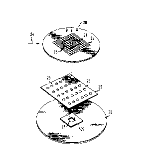
segment 21 as defined by mask grillage 22. Mask segment 21 is contained within
the optical field as represented by shaded mask region 23. Mechanical scanning in
the x direction (from left to right as shown) is represented by arrow 24. Orthogonal
5 scanning, in the y direction, may be sequential or simultaneous. The electronically
sc~nning beam for the stage shown, passes through one of apertures 25 in aperture
filter 26, with cross-over on the aperture filter plane to expose segment 27. Asimaged on wafer 28, consistent with image reduction, both segment 27 being
exposed and the optical field 29, again shown as a gray area, are reduced in size. As
10 depicted, filter 26 consists of x-skewed apertures to accommodate continuous,simultaneous, x-direction mechanical sc~nning This is in accordance with a likely
arrangement providing for continuous x-direction scanning of the mask and wafer,with y-direction stepping to accommodate a mask which is larger than the opticalfield in that direction as well. In accordance with this arrangement, there would be
15 no electronic sc~nning during y-direction mechanical movement. Alternatively,there may be provision for simultaneous y-direction mechanical s,~nning as well, in
which event, apellur~s 25 should be skewed in that direction as well.
The invention, as discussed, is dependent upon use of multiple-aperture
filter. In other respects, design may be in accordance with any of the variations in
20 the technical and patent lile,atu,t;. Design as appropliale to the invel~live ~e~hing,
as implemented on any such variation as well as future variations, is discllssed in
terms of FIG. 3. Apparatus shown includes a particle source 30, discussed as an
electron gun, delivering electron beam 31. collim~tQr lens 32 brings the initially
diverging rays into parallel relationship at 33 as shown. Scan deflection yokes 34
25 and 35 are responsible for electronic sc~nning, e.g. with continuous x-direction
sc~nning as resulting from one yoke. The second yoke provides for y-direction
movement, either continuous or as stepped intermediate x-direction scans. Mask 36,
as depicted again in terms of a preferred embodiment, is shown as segmented by
struts 37. Upon passing through the mask, the now pattern-corlt~ining beam 38,
30 comes under the influence of dynamic focus and stigm~tor yokes 39 and 40. As
suggested, focal length and other required adjustment at this stage may lessen
required mechanical movement. Stitching deflector yokes 41 and 42 provide for a
precision in placement of adjoining regions during x- and y-electronic
sc~nning/stepping.
~ ~ ~ 4 ~
Projection lens 43, as provided with variable access lens yoke 44, is
shown in the form of the now-pl~rellcd immersion variation, VAIL. Multiple
aperture filter 45 including apertures 46, in this instance shown as of reduce pitch
relative to mask 36, positioned on the crossover plane is at such spacing, X as to
5 result in a focused image on wafer 47 shown atop wafer stage 48. As discussed, for
illustrative purposes, mask 36 is shown as constituted of pattern regions corresponding
with strut-separated segments as in Canadian Patent No. 2,083,112, likely with the
embracing skirts, not shown, described in that case. ~ollowing modulation which
imparts patterning information on the beam during passage through mask 36, the beam
10 is converged, finally reaching a crossover (or image inversion) on or near the plane
defined by aperture filter 46. As discussed, the aperture filter is included for electron
im~gin~ for blocking unwanted scattered radiation as in SCALPEL. It may serve, as
well, to block other "noise" - e.g. by blocking unwanted feature-edge scattered
radiation.
As elsewhere in the disclosure, little emphasis is placed on apparatus
design features not directly relevant to the inventive teaching. As an example, an
aperture 46, included for the primary purpose indicated, may define - may itself serve
as - the numerical aperture (or pupil) of the system.
The projector lens system may include other elements, e.g. may include a
20 doublet of two optically equivalent lenses, in operation oppositely polarized to
inherently cancel corresponding aberrations implicit to design or operation common to
the two. (Consistent with usual practice, the hardware responsible for generation of
the functional shaped field is, itself, referred to as the "lens".)
As depicted, sc~nning is the primary responsibility of paired yokes 34 and
25 35 for x- and y-direction sc~nning. Such deflector pairs may serve, too, for precise
adjustment of beam position, to themselves, or together with other elements, assure
registration/alignment. Shown schematically as rectangles, they likely consist of
electromagnetic deflection coils, although they may be based on electrostatic
deflection, or a combination of both, as well. In either event, design criteria are well-
30 known - see, for example, Ludwig Reimer, "Transmission Electron Microscopy",
Springer Series in Optical Sciences, vol. 36, pp. 19-49.
Dynamic correction for aberration as well as for focusing, e.g. correcting
for wafer height variation as well as field curvature, is advantageously accomplished
by coreless lenses 39 and 40. Assigning responsibility for dynamic adjustment to35 these lenses speeds the process by lessening inductive lag time.
.-.a ~
~09~519
- 12-
Upon emerging from projection lens system 43, and passing through an
aperture 46, is made incident on wafer 47.
The system receiving experimental attention provides for mechanical
s~nning both of mask 13 and of wafer 27. For the system depicted - likely
5 conforming with first commerci~li7~tion - the first form of mechanical sc~nning may
be continuous, either the same or opposite in direction for the two, and at rates
accommodating dem~gnificfltion, e.g. at 4:1 to 5:1 for mask and wafer, respectively.
A second form of mech~nic~l movement provides for fabrication in which a single
mask pattern or region is stepped, to result in repeated exposure on the wafer. The
10 objective may be satisfied by movement of mask or wafer alone or a combination of
the two.
Design cAteria for col~len.ser and projector lenses and other parts of the
system, e.g. including scan coils and deflectors, are at an advanced state of design as
used, for example, in direct-write Electron Beam Exposure Systems as well as in
15 electron microscopy. (See, for example, Ludwig Reimer, "Tr~nsmi.~sion Electron
Microscopy", Sprin~er Series in Optical Sci~nces, vol. 36, pp. 1949. for design
con~i(ler~tions applopliate to the invenlive use.)
Reference is made to FIG. 3 in a general description of t'ne inventive
operation. While the figure is suitable for this purpose, it does not depict a variety of
20 elem~nt.~ f~mili~r to t'ne artisan and serving in actual operation. For example,
dynamic aberration correction may entail additional deflectors compensating for
errors resulting from equipmenV'process defects. Lens systems, too, are illustrative -
may include additional elements.
General
The inventive processes benefit by two attributes of charged particle
delineation as afforded by electrons, e.g. by use of SCALPEL, as well as by ions.
The first is the permitted reduction in wavelength - for electrons, to dimensions
perhaps one or two orders of m~gnit~l~e shorter than or competing electromagnetic
delineation - far shorter for ions. (The comparison is for x-ray in the design rule
30 regime of ~ 0.25 ~lm or smaller.) The second is the charged nature of the particles.
Together they permit the non-normal incidence of delineating radiation with respect
to the surface being patterned, and the facility for dyn~mi~ally adjusting
electronically to assure lithographic quality, e.g. registration/alignment as well as
focusing.
~4~ ~
- 13 -
Relaxation of demands related to depth of focus accommodates the
varying ray path length corresponding with instantaneous delineation of a pattern
region of significant area as operating from a fixed particle source - a source
conveniently considered as a point source. For contemplated near-term design rules,
5 perhaps down to 0.1 ,um, accelerating fields within the ~ 50-200 kV voltage range for
otherwise suitable apparatus design, imt~nt~neously exposed areas may be of a few or
several square millimeters, e.g. of 25 mm2. Such areas may correspond with segment
size, as otherwise dictated, for example, in accordance with one of the strut-supported
mask approaches of C~n~ n Patent No. 2,083,112. (The allusion, is to a square or,
10 more generally, to a low aspect-ratio rectangular segment. The effectively one-
dimensioned chip-length segment - the high aspect-ratio segment resulting from use of
non-intersecting parallel struts - profits both from this invention and from that of the
co-pending case as well.) Dynamic adjustment, as for positioning and focusing,
expedites stepping/sc~nning both with regard to continuous mask patterns and to
15 discontinuous patterns (e.g. strut/skirt separated patterns) and also expedites cell
projection (entailing repetitive use of one or more segments for part of or for the
entirety of an image or die).
It is convenient to consider the above embodiment, particularly in terms of
instantaneous overall segment exposure with dynamic adjustment for segment-to-
20 segment stepping. Other considerations may lead to variations. Wavelength/designrules may permit stepping, at least as between adjacent segments, without focusing
change - perhaps without positional adjustment. Circumstances may not require
segment-by-segment focusing change. Experimentally established conditions resulting
in optical field size of ~ 1 cm2 (for particular design rules and apparatus) permit a
25 significant number of segment-by-segment steps without refocusing.
A contemplated approach is based on ray scanning between or perhaps
serving the function of stepping. A likely application is in patterning of the "one
dimension", e.g. chip pattern length segment in which scanning may be, e.g. by means
of a beam of sufficient width to instantaneously expose the entirety of the short
30 dimension while scanning the long.
Discussion is largely in terms of exposure - likely cumulative exposure to
pattern a complete chip before moving on to the next. Other considerations may
dictate exposure to define a sequence of partial patterns - e.g. to define a
corresponding fractional region for one or more of the entire repeating series of such
35~ patterns in one dimension across an entire wafer - as directly or indirectly followed
~, ,
2094519
- 14-
by patterning of the adjacent fractional region, etc. Other conditions may be taken
into account in determining detailed operation. For example, minimi7~tion of
temperature differentials to reduce problems associated with mask or wafer
distortion may be accomplished by such repeated partial area exposures of individual
5 instantaneously exposed regions.
For the most part, beam sç~nning has been discussed in terms of the
fundamental objective - that of pattern exposure. Factors such as stage movement,
as well as a variety of distortiontaberration-inducing variations, may impose
demands requiring adjustment in sc~nning. For example, embodiments entailing
10 step-by-step exposure rather than continuous sc~nning, while in principle, requiring
no beam scanning or even mechanical sc~nning, during exposure of a given region
- may use, likely slower, beam scanning during exposure of a region to e.g. expedite
pattern stitching.
Illustrative Process Parameters
Process and apparatus are first discussed in terms of electron deiineation
- e.g. SCALPEL - for otherwise characteristic parameter values. To large extent,such values are determined by resist characteristics - primarily sensilivily - together
with source brig~tnPss and lens power. Values discussed are commenmrate with
presènt state-of-the-art availability. Experimental verification relates to an
20 individual mask segment size of lmm2. Depending on the position of the apellure
plate with respect to deflection fieldts, pitch (ape~ lure-to-apel lure spacing) is variable
within the combined permitted range of mask pitch and image pitch. As discussed,the relatively slow mech~nical movement required to reposition as between scan
areas of a given pattern, may be avoided under presently ~ in~ble conditions which
25 provide for optical field values sufficient to accommodate a total chip pattern.
Fabrication of devices to the small design rules contemplated places
large demands on precision. The inventive teaching, while most importantly
responsive to such needs, requires relative freedom from distortion - e.g. from
temperature-gradient induced distortion. At this time, region-by-region beam dwell
30 time, as required for convenient resist/particle bri~htnP..ss, is found to result in rate -
or, alternatively, in yield-consequential mask distortion if uncompensated. An
approach for alleviating this problem involves the more even heat distribution
accompanying repeated region-by-region partial chip exposures, discussed above.
Alternadve, as well as supplemental cooling, is useful. Apparatus approaches to
35 effectively accomplish the objective are known. Generally, it is sufficient to reduce
temperature gradient-induced distortion to ~ 20% of the design rule.
2094~19
- 15-
In summ~tion, particularly for small chip patterns, delineation of the
entirety of the pattern may entail but a single sc~nning step - but one optical field.
Depending upon the size of the optical field, delineation of a chip pattern of size
exceeding a single optical field may not require mech~nic~l movement - may be
5 accomplished with greater dependence on dynamic focusing. Under circumct~nces
where such pattern is of area which exceeds the optical field, delineation requires
mechanical movement as well as sc~nning- Required precision in alignment and
registration under these circllm~ct~nces is satisfied by accompanying field adjustment
in positioning of the beam. In fact, m~ch~nil~l movement, whether gradual or
10 stepwise, is generally accompanied by field adjustment. In the instance of pattern-
to-pattern, field adjustment in between independent patterns may be solely for
assurance of registration relative to previous and sequential patterning levels.Use of variable positioning of the optic axis, as noted, increases
operating margins. Use of permitted short deBroglie wavelengths - values perhaps15 as small or smaller than one-tenth of that theoretically required, as based on
wavelength limited resolution - increases freedom from a variety of causes. While
the invention provides for angle of in~i~em,~e for deline~ting radiation approaching or
equal to 90~, some deviation may be tolerated. Accordingly, while the advance does
not depend upon skewing as attendant upon sc~nning, needed precision with regard20 to landing angle (deviation from normal incidence or "skew") is relieved.
The intrinsic advantage afforded by att~in~ble depth of focus may
continue to accommodate height variations on the image plane. Such variations may
be the consequence of previous processing - as due to development following
exposure of preceding image levels.
25 Relationship Between Parameters
For one angular value of the numerical aperture, n.a., (as measufed at
the image plane - generally the plane of the wafer surface), depth of focus, D, of the
system in vacuum is given by:
D=+ EQ.4
8sin2 n-a
30 where ~ is the deBroglie wavelength of the particle beam, e.g. of the electron beam.
For small values of n.a this approximates to,
D= 05 2 EQ.5
n.a.
2094519
- 16-
For one set of proposed conditions, n.a. = 0.4 mrad and ~ = 0.045 A - a
value corresponding with an accelerating voltage of 70 kV - the numerical value for
depth of focus, D, is + 14 ~lm,
Small unintended mech~nical wafer movement is of little impact.
5 Permitte~ registration error resulting from non-orthogonal illumination of the wafer
may be calculated from the equation:
~h + e EQ 6
tana
in which:
~h = permitted variation in height, e.g. of the wafer surface
e = permitted maximum registration error from this source.
For 0.15 ~lm design rule, the total overlay budget (the total permitted
registration error) may correspond with the experimentally suitable 0.05 ~lm value.
~.csuming 0.01 llm error from this source, the permissible variation in landing angle
is tne value of a in EQ. 6.
In simplest terms, the inventive requirement regarding the multiple
aperture filter is satisfied by use of but two apertures. Satisfaction of aperture size
and spacing, as discllssed, permits doubling of image size without loss of resolution
associated with single aperture proces.cing. It is expected that most operation will
entail many apertures - at least one hundred. While variation is possible - and may
20 suit particular needs - ape~ s will ordinarily be equally spaced at least as regarded
in a particular rectalinear direction. As discussed in connection with FIG. 2,
apertures may be placed non-rect~line~rly - may be skewed in one or both directions
to accommodate simultaneous mechanical scanning - to accommodate continuous
mechanical scanning during electronic sc:lnning.
Basic relationships determinative of aperture size and spacing have bccn
set forth. Illustratively, in fabrication using design rules from 0.3 to 0.1 llm, con~rast
90% of that ~tt~in~ble for single aperture is retained for round apertures of diamet~r,
90 llm as spaced 250 llm. In general, consideration of fundamental as well as
practical factors, lead to likelihood of apertures in the diameter range of from ~ ~ m
to 360 llm as spaced at 100 ,um to 1000 ~lm, respectively.
Consistent with the approach taken, detailed information regarding
design and operation of a VAIL lens, or more generally a VAL lens, is not pr~nl~d
- reliance is had, for example, on the cited literature (as with other background
information not directly concerning the inventive advance). For brevity, the vari~hle
209~519
- 17 -
axis lens is considered as serving as a projection lens - likely the final imaging-
focusing lens before the wafer. While it is expected that the projection lens will
have provision for such positional adj~l~tment of its axis, it is possible that other
lenses in the system will be so provided as well. This may be t;ue of any other
S lenses in the im~ging system itself, as well as of any illumination lenses.