Note : Les descriptions sont présentées dans la langue officielle dans laquelle elles ont été soumises.
CA 02099299 1998-02-04
FREQUENCY SYNTHESIZER
FIELD OF THE INVENTION
The invention relates to a frequency
synthesizer, and more particularly to, a power saving
type of a local oscillation frequency synthesizer to be
used in a TDMA (time division multiplexing access)
system.
BACKGROUND OF THE INVENTION
In a TDMA system, an adjacent cell is
monitored during an idle slot in a communication frame
by changing a frequency from a presently using channel
to a channel which is considered to be appropriate in
the adjacent cell, and the formerly used channel is
restored by changing again the frequency. For this
purpose, a technology in which the switch-over of
oscillation frequencies is carried out with high speed
is required in the TDMA system.
A conventional frequency synthesizer used in
a TDMA system comprises a reference frequency
oscillation unit for generating a reference frequency
dependent on a carrier frequency, a voltage controlled
oscillator for generating a carrier frequency dependent
on an applied control voltage, a frequency division
circuit for dividing the carrier frequency by a fixed
division ratio, a phase comparator for comparing the
,,
CA 02099299 1998-02-04
.,_
reference frequency and a divided carrier frequency to
provide a phase difference therebetween, a charge pump
for charging and discharglng a capacitor by receiving
the phase difference, and a loop filter having a
capacitor to be charged pump for generating the control
voltage to be applied to the voltage controlled
oscillator, wherein the voltage controlled oscillator,
the frequency division circuit, the phase comparator,
the charge pump and the loop filter are connected to
provide a phase locked loop which is closed and opened
by a loop on/off switch.
In operation, the loop on/off switch is
turned on, and a power supply voltage is applied to the
reference frequency oscillation unit, and the frequency
division circuit and the phase comparator in the phase
locked loop, so that the voltage controlled oscillator
is applied with a control voltage from the loop filter
having the capacitor which is charged and discharged
dependent on the phase difference detected in the phase
comparator by the charge pump. Thus, a controlled
carrier frequency is generated in the voltage
controlled oscillator. Then, the loop on/off switch
is turned off to make the phase locked loop open, and
the power supply voltage is not applied to the
reference frequency oscillation unit, and the frequency
division circuit and the phase comparator in the opened
phase locked loop, so that the voltage controlled
CA 02099299 1998-02-04
.,.~ _.
oscillator is maintained to generate a carrier
frequency which is determined by an electric charge
voltage of the capacitor in the loop filter. Thus,
the phase locked loop is controlled to operate
intermittently, thereby realizing the saving of
electric power.
In the conventional frequency synthesizer
used in a TDMA system, the reference frequency is
changed dependent on a controlled carrier frequency
obtained in the voltage controlled oscillator, so that
the switch-over of channels having a small step width
is carried out, while a frequency division ratio of the
frequency division circuit is suppressed to be low.
Consequently, the switch-over of frequencies is
realized with high speed.
However, the conventional frequency
synthesizer has a disadvantage in that the loop
intermittent operation for the electric power saving is
limited to be carried out during a period in which the
switch-over of channels is not performed, because the
turning-off of the loop on/off switch to provide the
loop intermittent operation is difficult to be carried
out subsequently to the voltage stabilization of the
capacitor in the loop filter under the situation where
the switch-over of channels is performed in a TDMA
system by a short period. In more detail, the
capacitor in the loop filter is frequently charged and
CA 02099299 1998-02-04
-
discharged at a communication frame, during which
synchronism is set up with a separated frequency for
the switch-over of channels, by the charge pump. In
this situation, the capacitor takes a time in realizing
5 the voltage stabilization due to the occurrence of
dielectric absorption current flowing in the capacitor
immediately after the charge and discharge thereof.
SUMMARY OF THE INVENTION
Accordingly, it is an object of the invention
to provide a frequency synthesizer in which the
intermittent operation of a phase locked loop is
carried out with a sufficient time at a communication
frame.
It is a further object of the invention to
provide a frequency synthesizer in which the
intermittent operation fo a phase locked loop to be
carried out at a communication frame is realized
without inviting a complicated circuit structure.
According to the invention, a frequency
synthesizer, comprises:
a reference signal oscillation unit for
providing a reference signal;
a phase locked loop comprising a voltage
controlled oscillator for generating a carrier
frequency dependent on a control voltage applied
thereto, a frequency division circuit for dividing the
..,
CA 02099299 1998-02-04
carrier frequency to provide a divided frequency by a
predetermined division ratio, a phase comparator for
comparing the reference frequency and the divided
frequency to provide a phase difference, a charge pump
for applying a charging voltage and a discharging
voltage to a nodal point, a loop filter having a
capacitor connected to the nodal point for generating
the control voltage to be applied to the voltage
controlled oscillator, and a loop on/off switch for
closing and opening the phase locked loop;
a control unit comprising a power supply
control circuit for applying an operative voltage to
the phase locked loop which is closed by the loop
on/off switch which is turned on intermittently for a
switch-over of channels, a closed loop control circuit
for controlling the loop on/off switch to be turned on
and off in accordance with intermittent operation of
the phase locked loop, and a voltage control circuit
for controlling and application of a coarsely
controlled voltage to the voltage controlled oscillator
for the switch-over of channels in a communication
frame; and
a control voltage coarse adjustment circuit
for generating the coarsely controlled voltage to be
added to the control voltage of the capacitor in the
loop filter by a control of the voltage control
circuit.
~ .~,
CA 02099299 1998-02-04
BRIEF DESCRIPTION OF THE DRAWINGS
The invention will be explained in more
detail in conjunction with appended drawings, wherein:
Fig. 1 is a block diagram showing a
conventional frequency synthesizer to be used in a TDMA
system,
Fig. 2 is a block diagram showing a frequency
synthesizer in a preferred embodiment according to the
invention,
Fig. 3 is a block diagram showing a voltage
control circuit for a loop filter in the preferred
embodiment,
Fig. 4 is an explanatory diagram showing a
relation between a communication frame in a TDMA system
and an oscillation frequency required in the preferred
embodiment.
DESCRIPTION OF THE PREFERRED EMBODIMENTS
Before explaining a frequency synthesizer in
a preferred embodiment according to the invention, the
aforementioned conventional frequency synthesizer to be
used in a TDMA system will be explained in Fig. 1.
The conventional frequency synthesizer
comprises a reference frequency unit 1 for generating a
reference frequency, a phase locked loop 2 for
equalizing a carrier frequency to the reference
frequency, and a control unit 3 for controlling the
CA 02099299 1998-02-04
-
reference frequency unit l and the phase locked loop 2
to operate.
The reference frequency unit 1 comprises a
direct digital synthesizer 17 and a clock oscillator
18, wherein a reference frequency which is dependent on
a predetermined carrier frequency is digitally obtained
in accordance with a fixed clock frequency supplied
from the clock oscillator 18 by the direct digital
synthesizer 17.
The phase locked loop 2 comprises a voltage
controlled oscillator 5 for generating a carrier
frequency dependent on applied control voltage, a loop
filter 6 having a capacitor for generating a control
voltage to be applied to the voltage controlled
oscillator 5, a charge pump 7 for charging the
capacitor in the loop filter 6 by receiving a phase
difference between the reference frequency and a
divided frequency of the carried frequency, a frequency
division circuit 8 for providing the divided frequency
of the carried frequency, a phase comparator 9 for
providing the charge pump 7 with the phase difference,
and a loop on/off switch 10 for closing and opening the
phase locked loop 2.
The control unit 3 comprises a voltage
control circuit 11 for applying a power supply voltage
to the reference frequency unit 1, and the frequency
division circuit 8 and the phase comparator 9 in the
CA 02099299 1998-02-04
,. ..
phase locked loop 2 when the phase locked loop 2 is
closed for the phase locking operation, and an open
loop control circuit 12 for closing and opening the
phase locked loop 2 intermittently in synchronism with
the intermittent application of the power supply
voltage by the voltage control circuit 11.
Operation and a disadvantage of the
conventional frequency synthesizer have been formerly
explained.
Therefore, the explanation thereof is not
made here.
Next, a frequency synthesizer in the
preferred embodiment according to the invention will be
explained in Figs. 2 to 4, wherein like parts are
indicated by like reference numerals as used in Fig. 1.
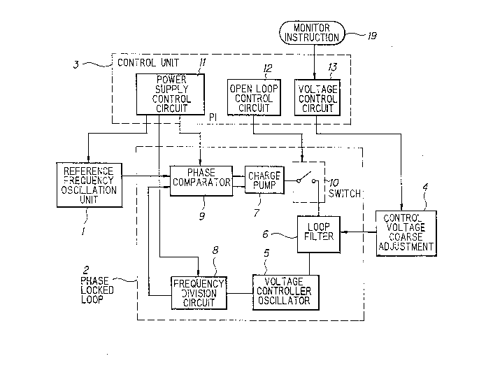
In Figs. 2 and 3, there is added to the
conventional frequency synthesizer a control voltage
coarse adjustment circuit 4 comprising a D/A converter-
voltage generator 15 for generating a coarse-adjustment
voltage and a capacitor 16 connected in parallel
between a capacitor 14 of the loop filter 6 and ground,
wherein the loop filter 6 comprises the capacitor 14
and resisters R1 and R2, and the control unit 3
comprises a voltage control circuit 13 for controlling
the control voltage coarse adjustment circuit 4 by
receiving a monitor instruction 19 additionally to the
conventional structure.
CA 02099299 1998-02-04
._ .
Fig. 4 shows a communication frame of 20ms in
a TDMA system comprising a receiving slot 21, a
transmitting slot 22 and an idle slot 23. In the idle
slot 23, a carrier frequency 20 i5 changed from a
frequency f1 for a channel presently used for a
communication including the receiving slot 21 and the
transmitting slot 22 to a frequency f2 for a channel to
be considered appropriate in an adjacent cell. Then,
when the carrier frequency f2 is not appropriate for a
communication as a result of monitoring the adjacent
cell, the carrier frequency f2 is restored for the
subsequent communication. Only in such cases as
changing the carrier frequencies fl and f2, a phase
lock loop is closed, and a power supply voltage is
applied thereto. On the other hand, when it is not
necessary to change a carrier frequency, that is, a
carrier frequency set up by an electric charge voltage
of the capacitor 14 in the loop filter 6 and a voltage
of the D/A converter voltage generator 15 is
maintained, no power supply voltage is applied to the
phase locked loop 2 which is opened by the loop on/off
switch 10.
Thus, the intermittent operation is realized
to save electric power consumption.
In operation, a carrler frequency of the
voltage controlled oscillator 5 is maintained by a
voltage obtained in the addition fo an electric charge
CA 02099299 1998-02-04
,.~,
--10--
voltage of the capacitor 14 in the loop filter 6 and a
voltage of the D/A converter voltage generator 15 in
accordance with the control of the voltage control
circuit 13, under the situation where the synchronism
is set up with a predetermined carrier frequency of a
communication channel.
Here, when the voltage control circuit 13
receives a monitor instruction 19, by which the carrier
frequency is changed to a carrier frequency of an
adjacent cell at the idle slot 23 in the communication
frame to check a receiving sensitivity of the adjacent
cell, the voltage control circuit 13 controls the
control voltage coarse adjustment circuit 4 to change a
voltage of the D/A converter voltage generator 15 by a
changing amount of ~V which is defined below.
~V=~X(fl-f2 )
Where fl is a frequency of a presently using
communication channel, fz is a frequency of a channel
to be monitored, and ~ is a modulation sensitivity.
Thus, a voltage applied to the voltage
controlled oscillator 5 by the loop filter 6 is
coarsely adjusted by the control voltage coarse
adjustment circuit 13, and a finely controlled voltage
is applied from the loop filter 6 to the voltage
controlled oscillator 5 by a phase difference of the
phase comparator 9. Consequently, the intermittent
operation of the phase locked loop becomes possible to
, . . .
CA 02099299 1998-02-04
be carried out for the electric power saving, because
the capacitor 14 of the loop filter 16 becomes
stabilized in a short time even during a remaining
short period at the communication frame after the
setting-up of synchronism with a carrier frequency.
The changing amount of the capacitor 16 in
the control voltage coarse adjustment circuit 13 is
small in an electric charge voltage between before and
after the switch-over of channels, so that the
influence of dielectric absorption current becomes
negligible in the preferred embodiment. Therefore, a
control voltage applied to the voltage controlled
oscillator 5 becomes stabilized in a time sufficiently
shorter than that in the conventional frequency
synthesizer, so that an electric charge voltage is
maintained without transient change, even if the loop
on/off switch 10 is turned off to make the phase locked
loop open. Consequently, a carrier frequency
obtained by the voltage controlled oscillator 5 is
maintained to be a predetermined value in cooperation
with a voltage of the D/A converter voltage generator
15 in the intermittent operation of the phase locked
loop 2.
After the adjacent cell is monitored, the
frequency is changed back to a carrier frequency for
the communication channel in the state where the loop
on/off switch 10 is turned on to make the phase locked
,~
\
CA 02099299 1998-02-04
loop 2 close. For this purpose, an output voltage of
the D/A converter voltage generator 15 is coarsely
changed to comply with a communical channel by the
control voltage-coarse adjustment circuit 13, and a
voltage of the capacitor 14 is finely changed to
provide the setting-up of synchronism with a carrier
frequency of the communication channel by the charge
pump 7 receiving a phase difference from the phase
comparator 9.
Although the invention has been described
with respect to specific embodiment for complete and
clear disclosure, the appended claims are not to be
thus limited but are to be construed as embodying all
modification and alternative constructions that may be
occur to one skilled in the art which fairly fall
within the basic teaching herein set forth.
. . ~