Note : Les descriptions sont présentées dans la langue officielle dans laquelle elles ont été soumises.
CA 02100153 2002-09-26
~1-
RCA 86,9951
APPARATUS FOl[hT_j~~ DjVISION MULTIPL~,,~jED PI~tOCESSING OF
FLUENCY DIV~:ON MULT1PI~~ED SIGNALS
This invention relates to apparatus for time multiplexed
processing of frequency multiplexed quadrature amplitude
modulated (QAM) signals.
The invention will be described in the environment of an
advanced definition television receiver (ADTV) of the type for processing
HDTV signals proposed by the Advanced Television Research Consortium
(ATRC), however it is to be understood that practice of the invention is not
io limited to such systems, but is applicable to other systems having
harmonically related amplitude modulated carriers.
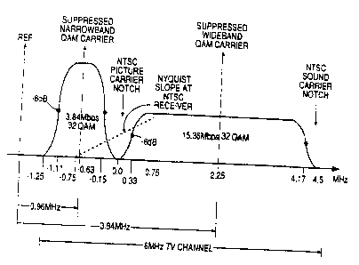
FIGURE 1 illustrates a television signal in the ADTV system
format. This signal is constrained to have a 6 MHz bandwidth in
conformance with NTSC standards. Unlike NTSC television signal however,
the ADTV signal consists of two quadrature amplitude modulated carriers,
one of which is located in the lower one quarter of the 6 MHz channel space
and the other which is located in the upper three quarters of the 6 MHz
channel space. The upper carrier has a bandwidth which is four times as
wide as the bandwidth of the lower carrier. The upper carrier frequency is
2o exactly four times the lower carrier frequency (related to a predetermined
reference). In the FIGURE 1 example both carriers are modulated 16 QAM.
FIGURE 2 illustrates a portion of a typical ADTV receiver
apparatus including the tuner IF and QAM demodulation circuitry. A
detailed description of this apparatus will not be herein provided but
z5 may be found in U.S. patent 5,287,180, issued February 15, 1994. What
is to be noted however, is the parallel processing circuitry (elements
118, 120, 122, 124, 126, 128, and elements 119, 121, 123, 125, 127, and
129) for processing the two QAM signals respectively. Each of these
parallel processing paths consist of relative large and complex, and
3o therefore expensive hardware. The present invention is directed toward
reducing such parallel hardware, in order to make such a system
affordable to the typical consumer. More particularly the invention is
directed toward utilizing processing apparatus in time division
RCA 86,951
-2-
multiplexed fashion to eliminate at least a portion of the parallel
processing circuitry utilized to process frequency division
multiplexed signals such as the two QA1~I signals illustrated in
FIGURE 1.
In accordance with the principles of the invention,
there is provided apparatus for processing a signal comprising a
plurality of QA~i signals in a channel. The apparatus includes
means responsive to the channel signal for separating the in-
phase and quadrature-phase components of ones of the plurality
of QAI~I signals. There are means responsive to the in-phase
components of the ones of the plurality of QAIvI signals, for
generating a time division multiplexed signal of the in-phase
components of the ones of the plurality of QAM signals. There is
also provided means responsive to the time division multiplexed
signal, for processing the time division multiplexed signal. And, a
utilization means conditions the processed signal for storage or
display.
2 0 BRIEF 3DESCRIP'I~OIOT ~F TI-IE DRAWINGS
FIGUREl is a graphical representation of the spectrum
of an A17T'il signal.
FIGURE 2 is a block diagrann of a portion of an HDTV
receiver including the tuner and QAIvI demodulation circuitry.
2 5 FIGURE 3 is a block diagram of circuitry for processing
plural QAM signals in a time division multiplexed embodying the
present invention.
FIGURE 4 is a block diagram of an FIR filter for the
time divisiota multiplexed filtering of two signals.
3 0 FIGURE 5 is a schematic diagram of one stage of the
filter of FIGURE 4.
FIGURE 6 is a timing diagram of respective clocking
signals for operation of the circuitry of FIGURE 5.
FIGURE 7 is a block diagram of the I, Q I~El'vTUX Al~
3 5 N1UX element 20 of FIGURE 3.
FIGURE 8 is a block diagram of an adaptive time
division multiplexed rotator circuit which may be implemented in
the element 24 of FIGURE 3.
-3- ~~~~~~~ RCA 86,951
Refer to FIGURE 3 which illustrates a portion of a more
cost effective ADT~I receiver. In FIGURE 3, a broadcast signal
having the spectral characteristics of the signal illustrated in
FIGURE 1 is applied to the tuner/IF circuitry 1U. The local
oscillator in the IF stage is selected to down convert the the center
of the standard priority (SP) channel to the SP channel's symbol
rate. The IF frequency is chosen to be 43.5 MHz, which places the
center of the baseband SP channel at 3.84 MHz. The down
converted ADTV signal is applied to an analog-to-digital converter
(ADC) 12. The ADC 12 is clocked at a rate of four times the SP
channel's symbol rate or 15.36 MHz. The sampling clock applied
to the ADC (and the other system clocks) are generated in the
clock element 14. Element 14 may include a VCXO incorporated in
1 5 a phase locked loop for phase locking the system clocks and the
sampling clock to one of the QAM carriers.
The 15.36 MHz samples generated by the ADC 12 are
applied to a low pass filter 16, having a pass band to attenuate the
wideband (SP) QAM carrier, and pass the narrower (HP) QAM
2 0 carrier. The lowpass filtered high priority (HP) samples are
applied to the circuit element 20, and to the subtrahend input
port of a subtracter 18. The 15.36 MHz ADTV samples from the
ADC 12 are applied to the minuend input port of the subtracter
18. The differences passed by the subtracter represent the SP
2 5 portion of the ADTV signal, that is the combination of the lowpass
filter 16 and the subtracter 18 provides a high or bandpass filter
function which attenuates that part of the spectrum occupied by
the HP signal component. The SP signal component provided by
the subtracter 18 is also applied to the circuit element 20.
3 0 Element 20 demodulates the respective I-IP and SP
QAM signals into their respective in-phase (I) and quadrature-
phase (Q) components. It also time division multiplexes the in-
phase components of the SP an HP signals, and time division
multiplexes the quadrature-phase components of the SP and HP
3 5 signals. The symbol rate of the SP signal is exactly four times the
symbol rate of the HP signal. In addition the ADTV signal was
sampled at four times the SP symbol rate ( 16 times the HP symbol
rate) and the sampling instants are phase locked to the SP carrier.
RCA 86,951
Therefore, alternate samples of the SP signal correspond to in-
phase and quadrature-phase signal components. The SP signal
may be separated to its in-phase and quadrature-phase
components merely by parsing alternate samples into an I signal
path and a Q signal path. The in-phase and quadrature-phase
components of the HIP signal may be separated by selecting every
fourth sample from the HP sample stream, and then parsing
alternate ones of these samples into an I signal path and a Q signal
path.
1 0 For every I (or Q) sample in the separated HP signal,
there are four I (or Q) samples in the separated SP signal. The SP
I or Q samples occur at a 7.68 ll~IHz rate and the HIP I or Q samples
occur at a 1.92 1VIHIz rate. Element 20 time division multiplexes
the I (Q) component samples at in the ratio of four SP samples to
one HIP sample, and couples the multiplexed I (Q) samples to a
lVyquist or symbol shaping filter 22.
FIGURE 7 illustrates exemplary circuitry for the
element 20. In FIGURE 7, the bandpass filtered SP signal from the
subtracter 18 is applied to a one-to-two multiplexer 30, and the
2 0 lowpass filtered HP signal is applied to the One-to-two multiplexer
31. Both the SP and HiP signals occur at the 15.36 IvIHIz rate. The
control inputs C, of the respective multiplexers 30 and 31 are
clocked at 7.68 .MHI~ conditioning the multiplexers to couple
alternate input samples to the I and Q output ports of the
2 5 respective rnultiplexers, thus separating the I atad Q components.
I~Tote, however, that even though the multiplexers 30 and 31
separate the I and Q components of the HIP and SP signals, the I
and Q signals are not demodulated as alternate samples which
correspond to 180 degree phases. Demodulation is performed by
3 0 multiplying successive I samples and successive Q samples by 1, -
1, 1, -1, 1, -1, 1, etc. This multiplication is performed by the
exclusive 10R gates XGR 35 and 36 which have first input ports
coupled to receive the I and Q samples and second input ports
coupled to a clock signal having a frequency of one half the output
3 5 sample rate from the multiplexers.
Demodulation need not necessarily be performed at
this point in the system. whether it is or not affects the form of
the succeeding filter functions. If demodulation is performed at
RCA 86,951
_5_
this point, the following Nyquist filters will have lowpass transfer
functions. Alternatively, if demodulation is performed after the
Nyquist filters, then the Nyquist filters will have bandpass
transfer functions.
The HP and SP in-phase components output from the
respective multiplexers are at a 7.68 MHz rate. The SP I samples
are coupled to a serial-input-parallel output shift register 32,
which shifts samples at the 7.68 MHz rate. Successive output
ports of the register 32 are coupled to the latter four input ports
of a five-input parallel-input-serial-output shift register 34. The
HP I samples are applied to a compensating delay stage 33 which
shifts samples at the 7.68 MHz rate. Output samples from the
stage 33 are applied to the fifth input port of the register 34. The
load input of the register 34 is pulsed at a rate of 15.36/8 MHz to
1 5 load a set of four successive SP and one HP I component samples.
The register 34 is then clocked at 9.62 MHz to provide a serial
stream of time division multiplexed SP and HP in-phase
component samples. The quadrature-phase samples are
separated and multiplexed in a similar manner with similar
2 0 circuitry (not shown).
The demodulated and multipi(exed I and Q samples,
from element 20, are applied to square root Nyquist filters 22.
The signal illustrated in FIGURE 1 is transmitted with excess
bandwidth, which bandwidth is tailored by Nyquist filters at the
2 5 transmitter. In order to minimize signal noise at the receiver, the
received signal is filtered with Nyquist filters having transfer
functions substantially matched to the Nyquist filters incorporated
at the transmitter. These filters are of the finite impulse response
(FIR) type and typically have 30 ox more taps and aSSOCiated
v
3 0 weighting circuits. Such filters are very hardware intensive.
Arranging the filters to operate in time division multiplexed
(Tl~l'~) fashion to process the time division multiplexed I and (2
samples significantly reduces the required hardware.
FIGURE 4 illustrates in block form an example of a
3 5 portion of one of the I and Q filters 22. The filter is arranged as
an input weighted FIR filter. Assume that the time multiplexed I
samples from the element 20 are applied to the bus designated
INPUT. These samples are applied to each of the weighting
RC.A 86,951
circuits Wn+i wherein they are weighted by respective coefficients
Cn+i. The weighted samples from the respective weighting circuits
are coupled to respective adders, which adders are interconnected
by delay stages DSp (Dgp). The delay stages are clocked at the
sample rate to successively process the applied samples, and
provide a filtered signal at the output at the right end of the filter.
Recall that the samples occur in the sequence SP, SP, SP, SP, SIP,
SP, SP, SP, SP, HP, etc. When an SP sample is applied to the input,
the delay stages Dip are enabled or clocked, and when an ~1P
sample is applied to the input the DHp delay stages are enabled or
clocked. In this manner the SP (I-IP) samples are filtered
independently of the SIP (SP) samples. Each time a particular
sample type SP (IMP) is applied to the input, only those delay
stages storing like type samples SP ()HP) are interconnected
between adder circuits forming a filter operative on only that
type sample. That is, when SP (HP) samples are applied to the
input, the Dgyp (Dsp) delay stages are effectively removed from the
circuit (the information contained therein hawever is retained).
The general timing of the two types of delay stages is shown in
2 0 the FIGURE and labelled Dsp CLDCI~ and Dhp CL~CI~ for the sample
sequence indicated above.
The system is illustrated with sources of weighting
coefficients Cn+i having two coefficients Cn+i and C'n+i, which
applies to the general case for a time division multiplexed filter.
2 5 In this instance the coefficients are switchable for the different
types of samples, if desired. That is, the filter may be arranged to
provide different transfer functions for the different signals by
using alternate coefficients for the different signals. Thus, if the
IIIP and SP signals are to be processed with different filter
3 0 functions, for example, the set of coefficients Cn+i (C'n+i) will be
applied to the weighting circuits Wn+i when the I-IP (SP) samples
are applied to the filter input. Switching of the coefficients is
effected by the coefficient control signal (e.g., signal CE of FIGURE
6).
3 5 FIGURE 5 illustrates in more detail exemplary circuitry
which may be implemented for the delay stages Dsp and DHp. The
circuitry shown is arranged to accommodate only one bit of the
signal samples. In practice a number of such circuits, equal to the
RCA 86,951
number of bits in the applied samples, will be arranged in
parallel. Clock and/or control signal waveforms required to
operate the FIGURE 5 circuitry are illustrated in FIGURE 6. In
FIGURE 6 the row of boxes designated SP, IIP etc represent sample
intervals and the respective sample type applied to the input of
the filter during respective sample intervals.
In FIGURE 5 the transistors T1, T2, T3, T7, and
inverters INV1 and INV2 form the circuitry of one bit of the Dsp
delay stage, and the transistors T4, T5, T6, T8, and inverters INV3
1 0 and INV4 form the circuitry of one bit of the Dgp delay stage.
Clock signal CSP1 is applied to the transistors TI and T3 to couple
the SP signal samples to inverter INV 1 from the preceding adder
and to couple SP signal samples from inverter INV2 to the
succeeding adder. The sample coupled to the inverter INV 1 is
I 5 stored on the stray capacitance Cs associated with the gate
electrodes of the inverter INV 1. The sample is retained on this
gate capacitance when the transistor T1 is turned off. Antiphase
clock CSP2 is applied to transistor T2 to condition T2 to couple the
output of the inverter INV 1 to the input of the inverter INV2.
Z 0 This occurs immediately after transistor T1 turns off. The sample
value applied to the inverter INV2 is stored on the stray
capacitance Cs associated with the gate f;lectrodes of INV2. During
the first half of a sample period n, INV~: is storing sample n-1 and
provides sample n-1 to the output adder during the portion of
2 5 sample period n that uansistor T3 is conditioned to conduct by
clock CSP1. Simultaneously sample n from the input adder 'is
applied to the inverter INV1 via transistor TI. Transistors TI and
T~ are turned off at about the midpoint of sample period n with
sample n being stored on the gate capacitance of INV 1 and sample
3 0 n-1 being output by INV2. During the second half of the sample
interval n, transistor T2 is turned on, coupling the output potential
of INV 1 to the gate electrodes of INV2, at which time both the
input to INV 1 and the output of INV2 exhibit the same potential
(corresponding to the state of sample n). Since the same potential
3 S occurs at the input of INV 1 and the output of iNV2, these points
may be interconnected to retain the potential thereon indefinitely.
~Iowever, in between successive sample periods it is not necessary
to make such connection to retain the sample information, as the
RCA g6,~51
_g_
gate capacitances are sufficiently large to hold the values at the
frequencies the samples occur. Transistor T7 is provided to make
such connection, but in this example T7 is only conditioned to
conduct during the sample periods that HP samples are applied to
the filter. Note that when transistors T1 and T3 are conditioned to
not conduct, the circuitry between transistors T1 and T3 is
effectively removed from the system, however the data stored
therein is not lost.
The circuitry of transistors T4 and T6 and the
elements therebetween operate in a similar fashion except they
are controlled by the clocks CIIPl, CI3I'2 and CB, and as can be
seen from FIGURE 6 are arranged to operate when the opposite
circuitry is idled.
Referring again to FIGURE 3, the output of the Nyquist
1 5 filter 22 is applied to an element 24 which may include an
equalizer and/or a deghoster. These functions may be performed
on the time division multiplexed signals from the filter 22. In an
embodiment of this type, the equalizer and deghoster may be
provided a reference basis corresponding to the time division
2 0 multiplexed signal for generating appropriate coefficients for the
correcting filters. Since such a deghosi:er and/or equalizer are
trained with reference to a time multiplexed signal, they may take
any of the known configurations. Alternatively, the I-iP and LP
samples may be demultiplexed and applied to independent
2 5 parallel equalizer and deghoster circuits, before being coupled to
decompression circuitry for storage or display.
Typically the input to circuitry such as contained in
element 24 will include further correction circuitry to compensate
for phase errors in the sampling clock applied to the AI)C 12. If
3 0 the sampling clock applied to the AI~C is not precisely phase
locked to the QAM carrier, then the I and Q samples provided by
the element 20 will contain errors even though they coraespond to
true quadrature components (though different from the desired
quadrature components). The further correction circuitry is
3 5 conventionally called a rotator or derotator. It can be shown that
any set of quadrature signals can be rotated to a desired angular
position by performing a complex multiplication on the
quadrature signals, i.e., quadrature signals I and Q can be rotated
~cA ~6,9s 1
-9-
to conform to corrected quadrature signals I' and Q' according to
the relation
I' = I cos(~) + Q sin()
Q' = Q cos(~) - I sin()
s where (p corresponds to the correction angle. Circuitry to perform
this correction is in general well known, and is illustrated in
FIGURE 8. The time multiplexed I and Q samples are applied to
respective input ports of a complex multiplier s0. Correction
coefficients (COS, SIN) from a coefficient generator s1 are applied
1 0 to a second set of input ports of the multiplier 50. Complex
products generated by the multiplier s0 are applied to a sliver s2
and an analyzer 53. Output signals from the dicer s2 are also
applied to the analyzer which generates a phase error signal
responsive to the signals occurring before and after application to ,
1 s the dicer. The phase error signal is integrated in the loop filter
s4, and thereafter coupled to the Coefficient generator s1 which is
programmed to provide appropriate correction factors
commensurate with the current phase errors. For a more detailed
description of this type of apparatus the reader is referred to the
2 0 text I~ICiITAL ~ONIIVIUNICA'TIONS, by Lee and llrlesserschmitt
(I~luwer Academic Publishers, Boston, ll~l,a., U.S.A., 1988).
In a system where the applied signals are time
division multiplexed certain adjustments must be made.
Nominally both the SP and HP samples will be multiplied by the
2 5 same coefficients, since they incurred tlhe same sampling phase
errors. I3owever the calculations of the correction coefficients are
complicated by the time multiplexed signals. One method of
generating the appropriate coefficients is to disable the analyzer
s3 on the occurrence of HP samples and perform the phase
3 0 analysis on only the SP samples. This is indicated in FIGURE 8 by
the application of the clock signal CB (FIGURE b) to the enable (E)
input of the analyzer s3. Since the SP samples occur 80 percent of
the time and are continuous over sets of four samples, fairly
accurate error calculations may be made. The negative aspect of
3 5 this method is a slight addition to the time required for
convergence.
A second method of calculating phase errors for the
time multiplexed signals is to generate independent error values
RCA 8b,951
-10-
for the HP and SP samples. Assuming that there is no delay
incurred in the dicer 52, independent error values may be
generated by providing parallel loop filters and directing the SP
errors provided by the analyzer 53 to one loop filter and the HP
errors to a second loop filter. The outputs provided by the
respective loop filters may then be selectively applied to the
coefficient generator 51 synchronous with the occurrence of HP
and ~P samples. lJxemplary apparatus to provide independent
error signals to the coefficient generator 51 is illustrated in the
block 55. If the block 55 is incorporated info the system, the
analyzer 53 will be continuously enabled rather than selectively
enabled by the signal CB. The signal Cl3 may however be employed
to selectively operate the multiplexing circuitry in the block 55.