Note : Les descriptions sont présentées dans la langue officielle dans laquelle elles ont été soumises.
WO 93/12603 PCI/US92/08057
2 ~ 2~
Frequency Translation Apparatus and Method
Field of the Invention
This invention generally relates to radio ~eceive~s and
more specifically to frequency trztn~l~tisn of digitized phase
information.
Background of the Invention
Typically, radio receivers include a reference osc~ tor.
The lafelellce os~ tor iB used to generate all the freqllP-nries
l 5 required to rlpmndtlktts the laceived ~i~n~l. If the phase of the
interms~ ts frequency (IF) signal will be directly tli~iti7etl,
then a ~letectQr lefelcllce signal must be ~ e~ated having a
frequency equal to the IF; otherwi6e, the digitized phase signal
will need to be corrected for the di~relellce in frequencies after
2 0 the digital detectisn. For e~ .le, ~sllme the radio receiver
has a lafe~ce osrill~tQr of 16.8 me~hertz (MHz) and an IF
(fi) of 456 kilnhsrtz (kHz). Using an N-bit phase digitizer
circuit operating at the lafel.:llce osr~ tor frequency (fref)
results in a digital ~lptect~r lefele~ce frequency (fO) equal to
2 5 fref divided by 2N. With a 6-bit phase ~ iti7er circuit, the
detector reference frequency would be equal to 16.8 MHz
divided by 25, or 525 kHz. Thus, the ~iigit~ etect~r ,efe~ellce
frequency (fO) does not equal the IF (fi). To directly digitize the
phase, the IF and the digital detector reference frequency must
3 0 be m~trhefl Two solutions are currently available.
First, another reference osr-ill~tor could be used to
generate a detector reference frequency equal to the IF. In the
previous eY~mple, the digital phase detector would require a
-
wo 93/12603 Pcr/US92/08057
2~ ~ 1527 2
second reference oscill~tor generating a frequency of 14.592
MHz (14.592t25= 456kHz). Several disadvantages result from
the use of the second .efelence oscill~tor. ~irst, a non-
st~nti~rd frequency would require a spe~li7.e-3 design and
S additional cost. ~Seconfl, an additional osçill~tor increases the
cost, size, and power consumption within the radio receiver.
Third, having two unique freqllP-n~es generated within the
radio receiver can pot~-nti~lly cause spurious interference
problems. Thus, ~rllling a .efele~lce osrill~tQr is an
10 ll~ e~irable solution to this problem.
A secon~l solution to the problem involves tr~n~l~tine the
frequency of the IF signal (fi) to match the frequency of the
etector reference (fO). This can be imrlçmPntRtl by miYing the
IF signal with a local osc~ tnr (L0) whose frequency is equal
1 5 to the difference fo - fi. Furthenng the precetline ey~mple~ the
IF of 456 kHz would need to be mi ed up ~uch that it was equal
to 525 kHz. The miYing would .eq~le an L0 frequency equal
to fo - fi, or 69 kHz. In ~.lfiit;nn to the estra hardware required,
this solution can also cause spurious interference problems.
2 0 ~ence, analog frequency tr~ncl~tion is also an lln~lesirable
solution to this problem.
Therefore, a need exists for a small, low cost, frequency
tr~n~l~ti~n device which does not require any additional
~n~log hardware or create any potp~nti~l spurious interference
2 5 problems.
Sllmm~ry of the Invention
The present invention encomp~sses a frequency
3 0 tr~ncl~tion apparatus for altering the effective frequency of the
phase infor n~tion of an input siEn~l The input signal has a
first phase (~(t)) and a first frequency (fi). The first phase (~(t))
is extracted and tli~iti7e~l at a secontl frequency (fO), for_ing a
WO 93/12603 PCI/US92/080~7
3 ~ J s~ ~
secQn-3 N-bit digital phase signal (~'(t)). The frequency
tr~n~l~tion apparatus generates a third digital phase signal
which applox;~ tes the difference between ~(t) and ~'(t).
Then, the frequency tr~n~l~tio~ apparatus comhines the
S secon-l digital phase signal and the third digital phase signal,
fol~i~g a fourth digital phase signal subst~ntiz~lly
approximating the first phase ~ignz~l
Brief Description of the Drawings
FIG. 1 is a block diagram of a radiotelephone system
which may employ the present inventiQn
FIG. 2 is a block diagram of a phase ~1Pmo~ ator in
accordance with the present inv~ntinn
1 5 FIG. 3 is a block diagram of a frequency tr~nclP.tinn
apparatu6 in accordance with the present invention
FIG. 4 is a graph of a detected phase signal prior to
frequency tr~n~l~tion
FIG. 5 is a graph of si~n~l~ cont~ine~l in the frequency
20 tr~n~l~tion apparatus.
FIG. 6 is a graph of a detected phase signal after frequency
trS~ncl~tion.
Description of a Preferred ~.mhorlim~nt
The l,.efe~led emho~imp-nt enComr~cses a direct phase
digitizer for use in a ~ ts.l receiver of a radiotelephone. The
direct phase digitizer uses a leceived signal having an
interm~ te frequency (fi) of 456 kHz. The radiotelephone
3 0 includes a reference 06~ r which generates a frequency
(fref) of 16.8 MHz. For a 5-bit phase digitizer, the effective
frequency (fO) is equal to 16.8 MHz/ 25 = 525 k~z. The phase of
the IF signal is directly digitized with the detector reference
wo 93/12603 Pcr/uss2/o8o57
2~5~7 4
frequency. The resulting raw phase word contains the desired
phase (~(t)), a constant phase offset (O, and a modulo-27t phase
error ramp function ([2~(fi fo)t]mod2~) The frequency
translation apparatus generates a frequency translation word
S cQnt~ining a modulo-2J~ phase ramp filnrtinn having equal but
opposite slope of the phase error ramp fllnctinn The frequency
tr~nRl~tion word is input into an N-bit adder together with the
raw phase word, s~lhEt~nt;~lly çlimin~ting the phase error
r~mp filnrt;on of the raw phase word.
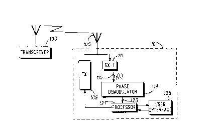
1 0 FIG. 1 is a block diagram of a radiotelephone system
which may employ the present invçntion- In the
radiotelephone system, the f~ed site transceiver 103 sends and
lac~:ives radio frequency (RF) sign~lR to and from mobile and
portable radioteleph-mes cQnt~ine-l within a fixed geographic
1 5 area served by the f~ed site transceiver 103. The
radiotelephone 101 is one such radiotelephnne served by the
fixed site transceiver 103.
Wbile receiving si~n~lR from the fixed site transceiver 103,
the radiotelephone 101 uses the ~nt,çnn~ 105 to couple the RF
2 0 signal and CO11V~11 the RF signal into an electrical RF sign~l.
The electrical RF signal is received by the radio receiver 111,
for use within the radiotelephone 101. The leceivt:r 111
generates the interme~i~te frequency (IF) signal 115. This
signal is input into the phase ~l~mo~lulator 119. The phase
2 5 ~lemo~ tQr 119 outputs a symbol signal 123 for use by the
processor 121. Processor 121 formats the symbol signal 123
into voice or data for the user interface 125. The user interface
125 cont~inR a microphnne, a spe~ker and a keypad.
Upon the tr~n~miRsion of RF sign~lR from the portable
3 0 radiotelephone 101 to the fised site transceiver 103, the voice
and/or data siEn~lR from the user interface are processed by
the processor 121. The processe-1 sign~lR are input into the
transmitter 109. The transmitter 109 CU11V~ ,S the data into
2101~27
s
electrical RF siFn~l~. The electrical RF si~n~TR are converted
into RF Ri~nAlR and output by ~nt~nn~ 105. The RF Rign~l~ are
received by the f~ced site transceiver 103.
FIG. 2 is a block diagram of the phase ~lçmo~ t~r 119 as
S illustrated in FIG. 1. The phase liçmo~ tor 119 includes a
limiter 301, a direct phase digitizer 303, an N-bit adder 313, a
phase proceRRin~ circuit 305, a symbol slicer 327, a reference
oR~ilk-tnr 315 and a frequency tr~ncl~tinn cir~it 317.
The limiter 301 le~ives the IF signal 115 and limits the
1 0 voltage range of the IF sigllal 115 to two voltage levels
correspQnAin~ to logic 0 and logic 1. The limiter 301 oulyut.S a
li~ited rF 8if~s~l 309. The l;~;le~l ~ signal 309,
A cos [2~l t + O(t)~,
i8 input to the direct phage ~i~iti7~r 303.
1 5The direct. phase ~i~iti7.4r 303 uses both the negative and
positive tr~nsitions (i.e. zero crossingR) of the limite~l IF signal
309 to s~m~e the internally generated modulo-2~ phase ramp
filnrtiQn A digital estim~te of the phase (~'(t)) 311 is formed by
~lPtecting the phase of the l~mited IF input signal 309 relative to
2 0 the phase of the tietect~r ~efe~a~ce (c(t)).
c(t) = cost27~0 t + ~]
- For an N-bit phase digitizer, the detector ~efe~ence frequency
(fo) is equ~l to fref~2N. In the preferred çmho~imPnt~ fref =16.8
Mhz, N = 5, and fo = 525 kHz. The N-bit e~tim~te~l phase word
2 S ~'(t) is equal to
~ '(t) = [~(th2~r(f~ - fo)t - ~lmo~
This rlP~tect~ phase word (~'(t)) cont~in~ the desired phase
infor_ation (~(t)), the phase error ramp f~m~tiQn (21~(fi - fo)t )
and the cQnFt~nt phase offset (O. Hence, if the intermP~ te
3 0 f~equency (fi) is not equal to the ~letect~r reference frequency
(fO), then there will be a phasè error ramp filnrtion which
must be removed to ensure accurate phase intell ~etation.
A'l''
2101527
The frequency tr~n.cl~tion circuit 317 generates a
frequency tr~n~l~tinn word (Ot(t)) 319 cont~ining a phase ramp
filn~inn having a glope which is equal and opposite to the slope
of the phase error ramp filn~ion~ namely
S ~t(t) = [2~(fo - fi)t ]m-yl~.
The frequency tr~n~ r.n word ~t(t) 319 and the raw phase
word 311 are input into the N-bit adder 313. The N-bit adder
313 romhines the two N-bit phase words 311, 319 resulting in
frequency tr~n~l~teA phase word (~(t) - 0 307.
1 0 The phase signal 307 i8 input into the phase processin~
unit 305. The phase ~locess;ng unit 305 removes the constant
phase offset (0. The phase proceEEing unit 305 cQnts~in~ either
a coherent phase processor or a di~eLe..ti~lly coherent phase
processor. In the y~eferlcd QmhoAim~nt~ a differentially
1 5 coherent phase proce~sor is used to remove the constant phase
(0. The resulting digital phase signal (~o(t)) 321 is the input to
the symbol slicer 327. The symbol slicer 327 ouL,~u~s the symbol
Aecicinn~ (data bits) correspo~ling to the phase sig~al 319.
FIG. 3 is a detailed block diagram of the frequency
2 0 tr~nsl~qtion circuit 317 illustrated in FIG. 2. The N-bit
frequency tr~n.~l~tion word 419 is generated using an N-bit
up/down counter 417 clocked by the reference oScillAtor 315. In
the pl~efel~ed emboAim~nt, the UID input 431 of the UplDown
counter 417 is set high so the mo~ltll~2~ phase ramp filnrtion
2 S 419 has a positive slope. If a negative slope is desired, then the
U/D input 431 should be set low.
The up-counter 401 and the co.~ A. ator 407 act together to
divide the detector lcfe~c~ce signal 421 by L. The lefelc-lce
signal 421 generated by the lefelellce os~ll~tor 315 drives the
3 0 up-counter 401. The up-coun er 401 oul~uls a word 423 to the
comp~rator 407. The compArator 407 has a pre-lo~etl value of
~1. When the counter word 423 equals L-1, the comp?.rator
407 generates an increment pulse 433 which resets ~he counter
~.
WO 93/12603 PCT/US92/08057
7 2:10~
401 and i8 input into the counter enable logc 409. Effectively,
the increment pulse 433 goes high every L cycles of the
reference osr~ tQr signal 421.
The up-counter 403 and the comr~rator 405 act together to
S divided the detector lefel~.ce oScill~tQr signal 421 by M. The
reference signal 421 generated by the reference oscillator 315
drives the up-counter 403. The up counter 403 outputs a word 429
to the comr~qrator 405. The cQmr~rator 405 has a pre-loaded value
of M-1. When the counter word 429 equals M-1, the comparator
405 generates an inhibit pulse 427 which resets the counter 403
and is input into the counter en~hle logic 409. li'ffectively, the
inhibit pulse 427 goes high every M counts of the reference
oscillator signal 421.
The counter en~hle logic 409 uses the increment pulse 433 and
1 5 the inhihjt pulse 427 to create a counter e.n~hle pulse 425. The
counter ~n~hle pulse 425 goes high every i~.c,~ ent pulse 433,
unless an inhibit pulse 427 has oc~ ~.ed ~ince the last increment
pulse 433. In order for the control en~hle logic 409 to be effective,
M must be greater than L. The counter çnQble logic 409 cont~inc 2
2 0 AND gates 411,415 and a set/reset (SR) flip-flop 413.
Each increment of the N-bit up/down counter 417 is equivalent
to ~ inE one phase ~ector (7C/2 N-l r~ nc) every L/f ref seconds to
the phase tr~nSl~tiQn word 419. The resulting frequency
tr~n~l~tion is representetl by the equation
~f=+/-fo/L.
The inhihit pulse 427 further improves frequency resolution of the
frequency tr~nCl~tion word 419 by inhibiting the increment
ol,e~d~ion once every M cycles of fref. Including the inhibit
function into the previous eq~l~tion~ the net frequency tr~n~l~tion
3 0 becomes
~f=+/-fotl/L- l~Il
The frequency tr~ncl~tion word 419 is comhined with the raw
phase word 311 to yield the frequency translated phase word 307.
wo 93/12603 Pcr/US92/08057
21Q1~27 8
The effective ~letectQr reference frequency after the addition of the
frequency translation phase word becomes
fo,eff = fo - f - fo [1 -/+ (V L - l/M)].
The frequency trqn~l~tion parameters L and M are selected to
yield the effective detector lefelence frequency which most closely
ayylo~;m~tes the desired intermediate frequency fi. In the
yrefe,led embo~imPnt~ L = 7, M = 87, and the effective ~letectQr
efe~e~ce frequency = 456.03448 k~7.
Note that both the inhibit and increment operations are not
n~ceSsz~ry for all applic-q-tiQn~. Some applit-qtions may require
only the increment oye~ation while others may require
multiple inhibit operqtinnc.
FIGS. 4, 5, and 6 are gr~q-phir~ql represçnt-qtiQn~
fl~monstrating the operation of the frequency tr~ncl~tion
1 5 circuit. FIG. 4 is a graph of the tletecte-l phase sector as a
filnrtinn of time. Graph 601 is a plot of the raw phase word 311
prior to frequency trq-n~lq-t;on of the ~ign~l, The inter~netli-qte
frequency of signal 501 was not equal to the ~let~ct~r reference
frequency; thus, the detected phase 501 differs from the actual
2 0 phase represçntetl by the dash line 503. FIG. 5 illustrates the
internal operation of the frequency tr~qn~l-qt;nn circuit 317.
Signal 507 is a represçntqtiQn of the nllmher of increment
pulses 433. Signal 509 is a represçnt~tion of the mlmber of
inhibit pulses 427. Signal 505 represents the frequency
2 5 trq-nclq-tion word 425. The frequency tr~n~l-qtiQn signal 505 is a
phase ramp filnrtion having a slope that is ~yy~ ;mqtely
equal and opposite to the slope of the ~etected phase signal 501.
FIG. 6 is an illustration of the detected phase at the ou~yu~ of
the N-bit adder 313. Signal 511 is a represent~tion of the
3 0 frequency tr~ncl~te-l phase word 307. Signal 513 is a
represent~tion of the actual phase of the limited IF input
signal 309. Close agreçment between the original phase signal
wo 93/12603 Pcr/US92/08057
9 2101~27
513 and the detected phase signal after frequency tr~n~l~qtion
511 is ~lprn~nctrated in FIG.6.
Described herein is an apparatus for effectively correcting
a known frequency offset of a digitally rletectefl phase fii
5 The offset is a result of the difference between the detector
reference frequency (fO) and the inter_ediate frequency (fi)-
This apparatus allow6 direct digiti7~tion of phase information
from an input signal without the addition of a gecon~l
frequency source in the radio Leceiv~r. The parameters L and
10 M are easily le~,o~lAmm~hle 60 they can tr?~nCl~te the
effective frequency of the digital detector indepP-n~nt of the
av~ hle reference frequency and interme~ te frequency.
This flPYihility iB an i~ol lant feature when applying this
apparatus to a radiotelephone which may have multiple
l 5 appli~qtiQnc. Additi~lly, the implPmPnt?~tiQn is simple, low
cost and effective.
What is cl~imetl i8: