Note : Les descriptions sont présentées dans la langue officielle dans laquelle elles ont été soumises.
. ,
21~3~J~ 2 10 3 4 0 5
CONSTANT CHARGE TIME OF DEFIBRIhLATION CAPACITOR
BACKGROUND OF THE INVENTION
The present invention relates to implantable cardiac
devices and more specifically to a system for charging a
defibrillation capacitor.
In implantable devices, such as defibrillators, it is
necessary to charge a capacitor to a desired level which is then
discharged to generate a defibrillation pulse. A battery is
provided in the implantable device to supply the energy for
charging the capacitor. As the battery becomes depleted, it has
been found that a longer time is required to charge the capacitor.
It is well known in the medical community that the longer it takes
to defibrillate once fibrillation onsets, the lesser are the
chances for recovery and survival. There continues to be a problem
between the battery voltage and charge time of the substantially
large capacitors used in defibrillation.
Systems are known for charging a capacitor. For example,
U. S. Patent No. 4, 586, 118 to Mihalka discloses a capacitor charging
circuit having means to compensate for changes in the capacitive
load as the capacitor is charged to maintain a constant peak
charging current irrespective of the capacitive load changes.
However, the system disclosed by Mihalka does not compensate for
variations in the power supply.
In the field of implantable cardiac treatment devices,
attempts have been made to compensate for depleted batteries. U.S.
Patents Nos. 4, 599, 523 to Pless et al . , 4, 590, 941 to Saulson et
2103405
al., 3,547,127 and 4,437,466 to Anderson, 3,759,265 and 3,746,005
to Thaler et al., 4,056,105 to Ravas, and 4,345,604 and 4,120,306
to Renirie disclose such systems in implantable cardiac pacer
devices. The Pless et al. patent discloses a priority switching
circuit for providing a minimum voltage to a voltage sensitive load
while charging a capacitor so that a battery supply is connected
to the capacitor whenever the voltage across the capacitor drops
below a preset value. The switching frequency varies with the
internal impedance of the battery.
The Saulson et al. and ('466) Anderson patents disclose
cardiac pacer systems having auxiliary or emergency batteries to
maintain constant pulse generation techniques when the main battery
becomes depleted. The ('127) Anderson patent discloses a cardiac
pacemaker having a regulated power supply to provide a current
independent of supply voltage over a large range of supply
voltages.
The Thaler et al. and Ravas patents disclose electronic
circuits to maintain a constant pulse width regardless of energy
source variations in pacemaking systems. __
The Renirie patents disclose cardiac pacers having power
source interface and switching circuits to achieve maximum
utilization of available source energy. Specifically, a DC
conversion circuit is provided to raise the value of the source
voltage to desirable values as a function of the source voltage for
driving an entire circuit or portions of a circuit.
2
203405
In the field of implantable cardioversion, by contrast
to pacing, it is necessary to charge a capacitor to relatively high
energy levels, one system has been developed to prevent loading
down supply voltage to other circuitry. Specifically, U.S. Patent
No. 4,548,209 to Wielders et al. discloses an implantable
cardioverter having charging circuitry including a supply voltage
detector which alters the time period of a timing circuit to
regulate the amount of current drawn by the primary of a
transformer; the secondary of the transformer being connected to
a cardioversion capacitor.
However, there is no system heretofore known which
operates to provide a constant charge time for a defibrillation
capacitor over substantially the entire life of the finite battery
supply.
SUMMARY OF THE INVENTION
It is a primary object of the present invention to
eliminate battery voltage as a factor of defibrillation capacitor
charge time.
It is a further obj ect of the present invention to charge
a defibrillation capacitor in a substantially constant period of
time over substantially the entire viable life of a battery.
The present invention comprises circuitry for charging
defibrillation capacitors in a constant period of time regardless
of battery voltage by employing a controlled duty cycle charging
technique. The defibrillation capacitors are charged in a
3
2103405
piecemeal manner through a transistor and flyback transformer
circuit. The gate of the transistor is driven by a constant
frequency pulse train in which voltage is conveyed to the
capacitors during one-half of the full cycle of the pulse train.
The product of the current and the voltage delivered to the
capacitors (voltage x current) is constant. Therefore, the current
increases as the voltage decreases and thus the charge time is
constant because the power is constant.
By providing a constant charging time, several advantages
are achieved. The viable life of the battery is increased because
less average current is drained from the battery. In addition,
because smaller average, as well as peak currents are used, the
associated circuit components may be smaller in size decreasing
overall size of the implantable package. A further consequence of
smaller currents is reduced heat generation and thus improved
reliability. Further yet, because charge time is constant, there
is no need to perform diagnostic follow up procedures on the
capacitor charge. Finally, by selecting a suitable charge time and
holding it constant when the battery is at full charge as well as
at further depleted levels, the probability of survival may
increase over the viable life of the battery. Still another
advantage is the use of a fixed charging frequency. A fixed
charging frequency is easier to isolate with a detector serving to
detect the charge signal.
4
210340 5
According to the invention, there is provided a capacitor
charging circuit for charging a defibrillation capacitor
comprising: battery supply means for providing a supply voltage;
defibrillation capacitor means for being charged to a predetermined
voltage; transformer means comprising a primary and a secondary,
the secondary being connected to the defibrillation capacitor
means, the secondary being charged by the primary for delivering
current to the defibrillation capacitor means; inverter means
connected to the battery supply means and to the primary of the
transformer means, the inverter means capable of assuming a first
state in which current is supplied from the battery supply means to
the primary of the transformer means and a second state in which no
current is supplied to the primary; inverter drive means connected
to the inverter means for generating an inverter drive signal
comprising repeating spaced pulses, each pulse of the inverter
drive signal triggering the inverter means to assume the first
state to supply current to the primary of the transformer means for
a duration corresponding to a duration of each pulse; and control
means connected to the defibrillation capacitor means, to the
inverter means and to the inverter drive means, the control means
monitoring the voltage across the defibrillation capacitor means
and monitoring the current in the primary of the transformer means
to terminate each pulse of the inverter drive signal in response to
the current in the primary reaching a preset value, and to
terminate the inverter drive signal in response to the voltage of
the defibrillation capacitor means reaching the predetermined
voltage, the control means controlling the inverter drive means to
maintain a frequency of the inverter drive signal constant so that
the energy delivered to the defibrillation capacitor means from the
secondary of the transformer means per cycle of the inverter drive
signal is constant.
The invention also provides a system for controlling the
charging and discharging of a defibrillation capacitor comprising:
battery supply means for providing a supply voltage; defibrillation
capacitor means for being charged to a predetermined voltage;
transformer means comprising a primary and a secondary, the
secondary being connected to the defibrillation capacitor means,
- 4a -
A
2~0340~
the secondary being charged by the primary for delivering current
to the defibrillation capacitor means; inverter means connected to
the battery supply means and to the primary of the transformer
means, the inverter means capable of assuming a first state in
which current is supplied from the battery supply means to the
primary of the transformer means and a second state in which no
current is supplied to the primary: inverter drive means connected
to the inverter means for generating an inverter drive signal
comprising repeating spaced pulses, each pulse of the drive signal
triggering the inverter means to assume the first state to supply
current to the primary of the transformer means for a duration
corresponding to a duration of each pulse; control means connected
to the defibrillation capacitor means, to the inverter means and to
the inverter drive means, the control means monitoring the voltage
across the defibrillation capacitor means and monitoring the
current in the primary of the transformer means to terminate each
pulse of the inverter drive signal in response to the current in
the primary reaching a preset value, and to terminate the inverter
drive signal in response to the voltage of the defibrillation
capacitor means reaching the predetermined voltage, the control
means controlling the inverter drive means to maintain a frequency
of the inverter drive signal constant so that the energy delivered
to the defibrillation capacitor means from the secondary of the
transformer means per cycle of the inverter drive signal is
constant: defibrillation trigger means connected to the
defibrillation capacitor means for triggering the discharge of said
defibrillation capacitor means to defibrillation electrodes;
termination means connected to the defibrillation capacitor means
for terminating the discharge of the defibrillation capacitor means
a preset period of time after the discharge of the defibrillation
capacitor means to the defibrillation electrodes by directing the
charge of the defibrillation capacitor means to ground; and
internal discharge means for connecting the defibrillation
capacitor means to ground upon desiring not to deliver a
defibrillation shock.
The invention also provides a method for charging a
defibrillation capacitor comprising the steps of:
- 4b -
A
21A3405
(a)providing a supply voltage;
(b) supplying current to a primary of a transformer during a
first half cycle from the supply voltage;
(c)charging a defibrillation capacitor from a secondary of
the transformer during a second half cycle;
(d)monitoring the level of the current in the primary of the
transformer and repeating steps (b)-(c) at a constant frequency
equal to the inverse of the sum of the first and second half
cycles, until the current in the primary of the transformer reaches
a preset value; and
(e)monitoring the voltage across the defibrillation
capacitor and repeating steps (b)-(d) until the voltage across the
defibrillation capacitor accumulates and reaches a preset value and
so that the energy delivered to the defibrillation capacitor per a
full cycle comprising the sum of the first and second half-cycles,
is constant.
According to a further aspect of the present invention,
there is provided a method for charging a defibrillation capacitor
comprising the steps of: providing a supply voltage;
intermittently connecting the supply voltage to a defibrillation
capacitor at a fixed frequency for a period of time during which
current is supplied to the defibrillation capacitor; monitoring
accumulation of voltage across the defibrillation capacitor as a
result of the step of intermittent connection; terminating the
intermittent connection of the supply voltage to the defibrillation
capacitor upon the voltage across the defibrillation capacitor
reaching a preset value whereby a constant amount of energy is
supplied to the defibrillation capacitor per a connection cycle of
the defibrillation capacitor to the supply voltage.
- 4c -
A.
210340
BRIEF DESCRIPTION OF THE DRAWINGS
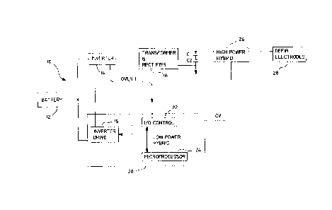
Figure 1 is a block diagram of the circuitry associated
with the constant charge time system of the present invention.
Figure 2 is a schematic diagram of the inverter circuitry
of the constant charge time system of the present invention.
Figure 3 is a detailed schematic diagram of a portion of
the circuitry illustrated in Figure 1.
Figure 4 illustrates the timing of various signals in the
constant charge time system of the present invention.
Figure 5 illustrates a comparison of the current in the
primary of the transformer when the battery is at full charge,
average charge, and depleted charge.
DETAILED DESCRIPTION OF THE DRAWINGS
Referring first to Figure 1, the constant charge time
system of the present invention is generally shown at 10. The
primary purpose of the system 10 is to charge the defibrillation
capacitors C1 and C2 by way of the battery 12. While two
capacitors are shown, it is possible to employ the present
invention for charging one or more than two capacitors.
Specifically, it is desirable to charge the capacitors C1 and C2
at a substantially constant rate over the entire life of the
battery 12.
In this regard, an inverter circuit 14 and transformer
16 are provided between the battery 12 and the capacitors C1 and
C2. The inverter 14 is driven by an inverter drive circuit 18
5
210340
formed as part of a low power hybrid circuit 20. As will be
described in more detail hereinafter, the inverter 14 essentially
comprises a transistor switch which is repeatedly triggered to
supply power from the battery 12 to a primary of the transformer
16. A secondary of the transformer 16 is charged by the primary
which in turn charges the capacitors Cl and C2.
The drive frequency of the inverter 14 is controlled by
the inverter drive circuit 18. In turn, the inverter drive circuit
18 is directly controlled by the I/O control circuit 22 via the
microprocessor 24. The I/O control circuit 22 monitors, among
other things, the voltage level on the defibrillation capacitors
C1 and C2 to terminate the delivery of an inverter drive signal
from the drive circuit to the inverter 14, when the microprocessor
programmed charge on C1 and C2 has been reached.
The high power hybrid circuit 26 is provided to gate the
voltage charged on the defibrillation capacitors C1 and C2 to the
defibrillation electrodes shown at 28. Microprocessor 24 is
responsive to parameters related to cardiac activity for
controlling the high power hybrid to pass the capacitor voltage to
the defibrillation electrodes 28.
Turning now to Figure 2, the inverter 14, high power
hybrid 26, and I/O control unit 22 are shown in more detail in
connection with the defibrillation capacitors C1 and C2. The
inverter drive 18, still shown in block form, is connected between
the I/O control unit 22 and the inverter unit 14. Generally, the
inverter 14 comprises a FET transistor Q1, which may be, for
6
2 10340 5
example, model No. MTPlONIOM sold by Motorola Corporation. The
inverter drive 18 controls the state of the transistor Q1 for
selectively supplying current through the drain D of the transistor
Q1 to the primary 16a of the transformer 16. Specifically, the
inverter drive 18 supplies pulses in the form of an inverter drive
signal at a preset frequency F to the gate G of the transistor Q1
to turn the transistor Q1 on. In an ON state, the transistor Q1
supplies current to the primary 16a while in an OFF state, no
current is supplied to the primary 16a. A pulse supplied by the
inverter drive 18 is terminated when the current in the mirror
resistor R1 reaches a preset value.
The current in the mirror resistor R1 which is connected
to the source of the transistor Q1 is fed to the I/O control unit
22 so that it may be continuously compared with a preset value.
In this regard, the I/O control unit 22 includes a comparison
amplifier 32, a current source 34, and resistor Rd connected to a
source of -6 volts. The current sensed from the mirror resistor
R1 is connected to one terminal of the amplifier 32 and the other
terminal of the amplifier senses voltage (WPREF) from the node
between the current source 34 and divider resistor Rd.
Inverter 14 also includes rectifier diodes D1 and D2 to
ensure that current built up in the secondary 16b of the trans-
former 16 charges the capacitors C1 and C2 to generate a voltage
which is positive at the node VC with respect to the ground
terminal connected to one terminal of the capacitor C2.
7
2103405
The high power hybrid circuit 26 includes, among other
sub-circuits not shown in Figure 2, two resistors R2 and R3 and
switch 42. Resistor R2 is of a substantially large value, such as
M ohms while resistor R2 is of a substantially small value, and
5 can be trimmed to achieve an accurate ratio between R2 and R3.
Resistor R3 is connected to a -3 volt source at one terminal
thereof. The voltage between resistors R2 and R3 is tapped and fed
to the I/O control circuit 22 via line 36. The voltage on line 34
is the voltage across the capacitors C1 and C2 and is termed CV.
10 I/O control unit 22 includes a comparison amplifier 38, a current
source 40 and resistor Rd. The line carrying the signal CV is
connected to one input of the comparator 38 and the other input
terminal of the comparator 38 is connected between the current
source 40 and the resistor Rd.
The output signals of comparators 32 and 38 are fed to
the microprocessor 24 for further processing as will be explained
in more detail hereinafter. Generally, however, the microprocessor
24 will cause the inverter drive 18, via I/0 control circuit 22,
to stop delivering drive pulses to the inverter 14 once the voltage
on the defibrillation capacitors has reached the value programmed
by the microprocessor by monitoring the signal CV. This is done
via the DRIVE CONTROL signal shown in Figure 2.
When it is desired to discharge the voltage stored on the
defibrillation capacitors C1 and C2, the microprocessor generates
a signal which closes the switch 42 in the high power hybrid
circuit 26. Once switch 42 is closed, the voltage across the
8
2 ~03~05
defibrillation capacitors is supplied to one of the defibrillation
electrodes 28a and 28b against the other so that an electric field
is generated throughout the heart between the electrodes 28a and
28b.
Figure 3 illustrates the inverter 14, inverter drive 18
and high power hybrid 26 in more detail. (The low power hybrid 20
is shown without the I/O control circuit 22 in Figure 3 for
simplicity.) The battery is represented as VB and is connected to
the source of the transistor Q1 and to the inverter drive 18. The
gate of transistor Q1 requires 10 volts or more to ensure low on
resistance characteristics. Because the drive signal supplied by
I/0 control 22 can go as low as 3 volts under transient conditions,
a gate boost circuit is necessary. In this regard, the inverter
drive 18 comprises transistors Q3 and Q4 which are connected so as
to form a complimentary inverter for the drive signal. Capacitor
C3 and diode D3 form a polarity inverter. Diode D4 and inductor
L1 are connected in series with transistor Q5 and form a LC voltage
doubler with the gate to source capacitance of Q1.
Under control of the DRIVE CONTROL signal, whenever
transistor Q4 is turned on, capacitor C3 is charged to the supply
voltage. On the other hand, when Q4 is turned off and Q3 is turned
on, the polarity of capacitor C3 is reversed and the drain of Q4
is grounded. Consequently, the inverted (positive rather than
negative) supply voltage is applied to the source of transistor Q5
to turn this transistor on. The combination of diode D3 and
inductor L1 guarantee that the gate of transistor Q1 is driven
9
2103405
positive with respect to the source at least three times the value
of the supply voltage because the source is at a negative
potential.
As shown in Figure 3, the inverter 14 further includes
capacitors C4 and C5 which together with the inductor L3 form a
filter to prevent high frequency current from flowing into the
battery. Transistor Q6 is connected across the gate of transistor
Q1 and together with diode D5 ensure that the actual gate voltage
does not exceed 10 volts with respect to ground so that the gate
of the transistor Q1 is protected when the battery is fresh (at
full capacity). Transistor Q2 returns the gate of transistor Q1
to VB to ensure that it turns off quickly.
The transformer 16 is a flyback transformer sized to
allow operation at a constant charge time over a wide supply range.
The charge time is chosen to be approximately 10 seconds with a new
battery which is assumed to put out 6.4 volts under no load. The
required inductance of the primary may be derived according to the
charge time chosen for maximum battery output. It has been found
that the required primary inductance is 10 microhenries. The
smallest possible core for the application of this transformer is
an RM4 core preferably formed of TDK H7C1 material which has a Bsat
of 4000 gauss at 40 degrees Celsius.
The secondary circuit of the transformer 16 and the
capacitors C1 and C2 are charged in parallel even though they are
connected in series with respect to the switch 42 of the high power
hybrid 26. As a result, there is no need to "balance" the
210340 5
capacitors to provide even voltage distribution. When the
capacitors are discharged, diodes D7 and D8 insure that the larger
of the two capacitors does not reverse the polarity of the smaller
capacitor.
The high power hybrid circuit 26 is designed to convey
the charge on the capacitors C1 and C2 to the defibrillation
electrodes 28a and 28b when the microprocessor issues a
defibrillation control signal. Discharge sub-circuit 50 includes
a transistor Q7 and resistor R5 which form a discharge path for the
stored energy on the capacitors C1 and C2 in the event that it is
necessary to charge the capacitors without delivering a pulse to
the patient. Sub-circuit 50 includes an SCR Q7 and associated
biasing resistor and diode (not labelled) that discharges
capacitors C1 and C2 internally if therapy is not required: This
is achieved by triggering the SCR Q7 to discharge the capacitors
C1 and C2 through resistor R5. Terminate sub-circuit 52 includes
an SCR Q8 (and associated biasing diode and resistor) for
truncating the defibrillation pulse delivered to the patient by
discharging the capacitors C1 and C2 directly to ground. Sub-
circuits 50 and 52 are controlled by the low power hybrid 20 as
will be explained hereinafter. Resistor R6 limits the discharge
current to prevent internal damage.
The switch 42 is embodied as a silicon rectifier Q9, the
gate of which is connected to transformer T2. Transformer T2 is
provided for firing the SCR Q9.
11
210340 5
As aforementioned, the voltage across the capacitors C1
and C2 is sensed through resistors R2 and R3. Diode D9 is provided
to protect the system circuits in the event that R3 opens. A
negative 3 volt reference is applied to the resistor R3 which is
the same as that used as a reference to the comparator 38 via
resistor Rd (Figure 2). Thus, both inputs to comparator 38 are
(indirectly) referenced to negative 3 volts to allow current source
40 to be programmed to zero while the comparator still has headroom
for operation.
The low power hybrid circuit 20 further includes a
discharge driver circuit 54, a terminate driver circuit 56, a
defibrillation trigger circuit 58 and a fault detection circuit 60.
The discharge driver circuit 54 comprises transistor Q10 and
capacitor C8 (together with associated biasing circuit elements).
By bringing a signal on the line labelled DISCHARGE low, the SCR
Q7 of the discharge circuit 50 is grounded so that the charge on
the capacitors C1 and C2 will be diverted through resistor R5 and
SCR Q7 of the discharge sub-circuit 50 to ground.
The defibrillation trigger circuit 58 and the terminate
driver circuit 56 are used to deliver a defibrillation or
cardioversion pulse. The terminate driver circuit 56 comprises a
transistor Q11 (and associated gate drive circuit components) which
is connected via a capacitor C9 to the terminate sub-circuit 52 in
the high power hybrid 26. Similarly, defibrillation trigger
circuit 58 comprises a transistor Q12 (and associated gate drive
12
~._ 210340 5
circuit components) which is connected via capacitor C10 to the
transformer. T2.
When the microprocessor 24 determines that it is
necessary to deliver a defibrillation or cardioversion pulse, the
signal on the DEFIB line is pulled low. This turns transistor Q12
ON which discharges capacitor C10 through the pulse transformer T2.
As a result, SCR Q9 is turned on and the charge on the capacitors
C1 and C2 is delivered to the defibrillation electrodes via lines
62 and 64. When the defibrillation pulse reaches approximately 1/3
of its initial value, the signal CV is sensed by the microprocessor
through the I/O circuit 22. The microprocessor responds by
generating a signal on the TERM line to turn ON transistor Q11.
This discharges capacitor C9 through the gate of transistor Q8
which shorts the capacitors C1 and C2 to ground through resistor
R6 (approximately 2 ohms).
The fault detection circuit 60 comprises transistor Q13,
the emitter of which is connected to a resistor-diode combination
R10-D7. The fault detection circuit 60 is connected to the output
line 64 in the high power hybrid 26 via resistor R11. In the event
that the transistor embodying switch 42 becomes shorted, the output
of the charging current would flow through the heart. However,
some of this current would also flow through resistor R11 and the
emitter-base junction of transistor Q13 bringing the signal of the
FAULT line high. The microprocessor senses the status on the FAULT
line through the I/O control circuit 22 and shuts down the inverter
14 at once if switch 42 shorts.
13
_ 2~~3~~5._
The operation of the constant charge time mechanism will
now be described with reference to Figures 2, 3 and 4. Generally,
the constant charge time mechanism operates by charging the
capacitors C1 and C2 in increments by repeatedly charging the
primary of the transformer 16 to a peak current value. As the
battery supply voltage VB decreases, the primary current takes
longer to reach the peak value. However, the drive waveform is
turned off by circuitry which senses the current through the mirror
resistor R1. Therefore, the peak current in the primary will
remain constant regardless of the supply voltage.
The inverter drive signal generated by the inverter drive
circuit 18 under control of the microprocessor is supplied to the
gate of transistor Q1. The amplitude of the inverter drive signal
must be approximately 10 volts to drive the gate of the transistor
Q1. In response to the 10 volt pulse of the inverter drive signal,
a current is generated in the primary of the transformer 16. The
level of the current IPR~ in the primary is sensed via the mirror
resistor R1 and reflected as a voltage hereinafter referred to as
OVER I. The current in the mirror resistor is a known fraction
(1/1000) of the current in the primary of the transformer 16.
OVER I is compared in the comparator amplifier 32 with a preset
reference level ISEr of 0.4 V.
Once the OVER I voltage reaches the preset reference
level, the microprocessor terminates the positive portion of the
inverter drive signal via the DRIVE CONTROL signal. The current
in the secondary of the transformer ISEC Jumps to a maximum value at
14
2103405
the maximum of the current in the primary, and then begins to
decay. As a result, the voltage VC across the capacitors C1 and
C2 rises in response to the current in the secondary of the
transformer. However, once the current in the secondary returns
to zero, the voltage across the capacitors stops rising. The
signal CV representing the capacitor voltage is constantly
monitored in the I/O control 22 and compared with the programmed
final voltage level of the capacitors, hereinafter referred to as
WPREF. At the next occurrence of a positive pulse in the inverter
drive signal, the mechanism repeats and the voltage across the
capacitors C1 and C2 (VC) rises from the previously charged level
to a higher level. When the voltage across the capacitors reaches
the final level set by WPREF, the comparator 38 issues a pulse as
shown in Figure 4 which is detected by the microprocessor to
terminate the DRIVE signal. The level of WPREF is programmable
(via the current source 40) from 0 to 2.4 volts (DC) (or -3 volts
to -0.6 volts with respect to the -3 volt reference) creating an
energy output of 0.1 to 34 Joules.
The energy stored in the primary of the transformer each
cycle of the drive signal is equal to 1/2LIPK where L is the
inductance of the primary 16a of the transformer 16. Assuming
ideal conditions with ideal inductors and zero ohm switches, the
on-time toN is equal to IPKL/VBAT SO that IPK is equal to VBATtoN/L. If
the frequency of the drive signal is maintained constant, then the
energy delivered to the capacitors per cycle is constant, the
result being that the charge time of the capacitors is constant.
2103405
The value toN in the foregoing equations represents the time needed
for the current in the primary (IPRI) to reach IPK. Particularly,
because the capacitor is charged. in increments (Figure 4), the
total time to charge the capacitors is the sum of the charge time
for the charging increments. Thus, by ensuring that the current
in the primary of the transformer reaches a peak level within a
constant period of time, the charging increments are effected in
a constant period of time. In effect, the battery power supply is
intermittently connected to the capacitor at a fixed frequency.
Shown in Figure 5 is a comparison of the current in the
primary 16a of the transformer 16 at three different approximate
battery voltages. When the battery is new and thus at high
voltages, the current in the primary will reach the peak value more
quickly than when the battery voltage is at an average level or a
depleted low level. As aforementioned, however, the inverter drive
signal is terminated according to the current through the mirror
resistor R1 via the DRIVE CONTROL signal from the microprocessor
24. Thus the peak current will remain constant regardless of
battery voltage.
The above description is intended by way of example only
and is not intended to limit the present invention in any way
except as set forth in the following claims.
16