Note : Les descriptions sont présentées dans la langue officielle dans laquelle elles ont été soumises.
21~474~
SEI 93-18
1 TITLE OF THE INVENTION
Field Effect Transistor
BACKGROUND OF THE INVENTION
Field of the Invention
The present invention relates to a Schottky-barrier
type field effect transistor (MESFET) and, more
particularly, to a dual-gate type field effect transistor
(FET) having two gate electrodes between a source and
drain electrodes.
Related Background Art
With the recent rapid development in information
network systems, the demands for satellite communication
systems have been rapidly increasing, and the frequency
band is getting higher and higher. A high-frequency FET,
especially a MESFET consisting of GaAs, has been put into
practical use as a transistor which can overcome the
characteristic limit of a silicon bipolar transistor
conventionally used in a high-frequency circuit.
In order to realize a high-output, high-efficiency
GaAs MESFET, it is important to decrease the resistance
hetween the source and gate electrodes, i.e., the source
resistance (Rs), and increase the transconductance (gm)
while increasing the drain breakdown voltage between the
gate and drain electrodes.
In a dual-gate type MESFET, in order to increase the
drain breakdown voltage, the drain-side gate electrode,
21047~5
SEI 93-18
1 i.e., the second gate electrode, may be formed apart from
a high-impurity-concentration ion implantation region on
the drain electrode side.
In this case, a gate elongation effect is caused to
increase the effective gate length in a range where the
gate bias is low, i.e., a range where the gate bias is a
negative value close to 0 V if the FET is n-channel FET.
As a result, the transconductance gm of the FET is
decreased in the range.
SUMMARY OF THE INVENTION
It is an object of the present invention to increase
the drain breakdown voltage of a dual-gate type MESFET
without decreasing the transconductance gm.
In order to achieve the above object, a field effect
transistor of the present invention comprises a
semiconductor substrate having a non-doped buffer layer,
a thin first pulse-doped layer with a high impurity
concentration, and a cap layer sequentially formed on an
underlying semiconductor substrate by epitaxial growth.
The cap layer has a thin second pulse-doped layer with a
high impurity concentration sandwiched between non-doped
layers. The second pulse-doped layer has a thickness and
an impurity concentration set such that the second
pulse-doped layer is depleted by a surface depletion
layer caused by interface state of a surface of the cap
layer, and the surface depletion layer does not extend to
210~74~
SEI 93-18
1 the first pulse doped layer. A source electrode, a drain
electrode, and first and second gate electrodes are
formed on a surface of the semiconductor substrate.
High-impurity-concentration ion implantation regions are
formed at a source electrode formation rPgion, a drain
electrode formation region, and a region between the
first and second gate electrode formation regions to
extend from the surface of the semiconductor substrate to
the first pulse-doped layer. The second gate electrode
formed on the drain electrode side is separated from the
high-impurity-concentration ion implantation region
below the drain electrode.
When the second gate electrode is separated from the
high-impurity-concentration ion implantation region on
the drain electrode side, a surface depletion layer due
to the interface state of the substrate surface is formed
in the separated portion as well as in a portion below the
second gate electrode. However, extension of this
surface depletion layer in the direction of depth is
prevented by the second pulse-doped layer in the cap
layer. Consequently, the first pulse-doped layer as a
channel layer i8 free from the influence of the surface
depletion layer, and only the depletion layer immediately
below the second gate electrode has an effective
influence on the channel layer. That is, no increase in
effective gate length occurs. Therefore, no reduction in
21~47~
SEI 93-18
1 the transconductance gm on the low-gate-bias range
occurs, and the transconductance gm becomes constant with
respect to a wide range of changes in gate bias.
The present invention will become more fully
understood from the detailed description given
hereinbelow and the accompanying drawings which are given
by way of illustration only, and thus are not to be
considered as limiting the present invention.
Further scope of applicability of the present
invention will become apparent from the detailed
description given hereinafter. However, it should be
understood that the detailed description and specific
examples, while indicating preferred embodiments of the
invention, are given by way of illustration only, since
various changes and modifications within the spirit and
scope of the invention will become apparent to those
skilled in the art form this detailed description.
BRIEF DESCRIPTION OF THE DRAWINGS
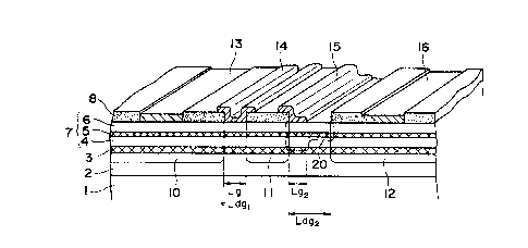
Fig. 1 is a perspective view showing an exposed
cross-sectional surface according to the first embodiment
of the present invention;
Fig. 2 is a sectional view showing the second
embodiment of the present invention;
Fig. 3 is a sectional view showing the third
embodiment of the present invention;
Fig. 4 is a sectional view showing the fourth
210~74S
SEI 93-18
1 embodiment of the present invention;
Fig. 5 is a sectional view showing the fifth
embodiment of the present invention;
Fig. 6 is a sectional view showing the sixth
embodiment of the present invention; and
Fig. 7 is a sectional view showing the seventh
embodiment of the present invention.
DETAILED DESCRIPTION OF THE PREFERRED EMBODIMENTS
A dual-gate MESFET according to an embodiment of the
present invention will be described first with reference
to Fig. 1. A non-doped GaAs buffer layer 2 is formed on a
semi-insulating GaAs semiconductor substrate 1. This
buffer layer is formed by a crystal growth technique such
as the MBE method (molecular beam epitaxy method) or the
OXVPE method (organic metal vapor phase epitaxy method).
In order to improve the carrier trapping property of a
channel layer 3 (to be described later), the conductivity
type of the buffer layer 2 is set to be p conductivity
type by controlling the supply ratio of a Group V material
to a Group III material. The carrier density of the GaAs
buffer layer 2 is set to be, e.g., 2.5 x 10l5 cm~3.
An Si-doped n-type first GaAs pulse-doped layer 3 is
formed on the buffer layer 2. The pulse-doped layer 3 has
a high carrier density, 4 x 10l5 cm~3, and a small
thickness, 200 A. A cap layer 7 constituted by a
non-doped GaAs layer 4, a second GaAs pulse-doped layer
s
210474~
SEI 93-18
1 5, and a non-doped GaAs layer 6 is formed on the
pulse-doped layer 3 by a crystal growth technique such as
the MBE method or the OMVPE method. The non-doped GaAs
layer 4 is of n conductivity type and has a carrier
density of 1 x 10l5 cm~3 or less, and a thickness of 150 ~.
The second GaAs pulse-doped layer 5 is an Si-doped layer
of n conductivity type, which has the same high carrier
density as that of the first pulse-doped layer 3, i.e., 4
x 10la cm~3, and a thickness of 50 ~. The non-doped GaAs
layer 6 is of n conductivity type and has a carrier
density of 1 x 1015 cm~3 or less and a thickness of 200 ~.
The thickness and impurity concentration of the
second GaAs pulse-doped layer 5 are set such that the
second GaAs pulse-doped layer 5 is depleted by a surface
depletion layer caused by the interface state of the
substrate surface, i.e., the surface of the non-doped
GaAs layer 6, and the surface depletion layer does not
extend to the first pulse-doped layer 3.
Gate electrodes and high-impurity-concentration ion
ZO
implantation regions are formed on the epitaxial wafer
having such a laminated structure by a self alignment
technique or the like. In addition, a source electrode
and a drain electrode are formed on the wafer.
High-impurity-concentration ion implantation regions 10
to 12 are formed by two steps below. The first step i9
forming first and second dummy gates (not shown),
21047 4~
SEI 93-18
1 consisting of a photoresist, on first and second gate
electrode formation regions. And the second step is
implanting Si ions using the first and second dummy gates
as masks. Thereafter, an inorganic insulating film such
as an SiO2 film is deposited on the entire surface of the
resultant structure. The SiO2 film is lifted off by using
the first and second dummy gates to form an SiO2 film 8
having openings in the first and second gate electrode
formation regions. Portions, of the SiO2 film 8, which
correspond to source and drain electrode formation
regions are removed, and deposition of an Ohmic metal and
a lift-off process are performed, thus forming a source
electrode 13 and a drain electrode 16. Deposition of a
Schottky metal and a lift-off process are performed to
form first and second gate electrodes 14 and 15.
A gate length L~2 of the second dummy gate on the
drain side is set to be larger than a gate length L~l of
the first dummy gate on the source side. The first gate
electrode 14 overlaps the high-impurity-concentration
ion imptantation regions 10 and 11 through the SiO2 film
8, whereas the second gate electrode 15 overlaps only the
high-impurity-concentration ion implantation region 11
through the SiOz film 8. With this structure, the first
gate electrode 14 has a so-called self-aligned structure
with respect to the high-impurity-concentration ion
implantation regions 10 and 11 so that a gate length LB1
2 1 0 4 7 ~ ~
SEI 93-18
1 can be shortened to the limit of a lithographic technique
used in the formation of a dummy gate. In addition, the
second gate electrode 15 can be sufficiently separated
from the high-impurity-concentration ion implantation
region 12 on the drain side.
According to the dual-gate type MESFET having the
above-described arrangement, since the second gate
electrode 15 is sufficiently separated from the
high-impurity-concentration ion implantation region 12
on the drain side, the drain breakdown voltage is high.
Furthermore, since the cap layer 7 in this separated
portion includes the second GaAs pulse-doped layer 5, the
gate elongation effect due to a surface depletion layer
can be suppressed. Therefore, the effective gate length
in the second gate electrode 15 is almost equal to a gate
length L~2, and hence can be sufficiently reduced to a
length almost equal to the gate length of the first gate
electrode 14 having the self-aligned structure. A
depletion lay~r 20 in Fig. 1 is in a state wherein a
negative gate voltage is applied to the second gate
electrode lS. As is apparent from Fig. 1, the depletion
layer 20 constricts the channel (first pulse-doped layer
3) only at a position immediately below the second gate
electrode 15. A portion of the depletion layer 20 between
the second gate electrode 15 and the
high-impurity-concentration ion implantation region 12
210474~
SEI 93-18
1 is caused by the interface state of the surface of the cap
layer 7 and is prevented by the second pulse-doped layer 5
from extending downward. When a high-frequency signal is
input to only the first gate electrode 14, and the second
gate electrode 15 is used for gain control, the gate
length Lg2 f the second gate electrode 15 need not be
reduced so much as in the above case. Thus, the
manufacturing yield of the MESFET of the embodiment
applied in such a manner is very high. When the second
gate electrode 15 is separated from the
high-impurity-concentration ion implantation region 12
on the drain side, a drain conductance gd becomes small.
Since the gain of an FET increases with an increase in
gm/gd, an FET having a high gain can be manufactured.
Figs. 2 to 7 are sectional views showing the second
to seventh embodiments of the dual-gate type MESFET of
the present invention. The same reference numerals in
the second to seventh embodiments denote the same parts
as in the first embodiment, and a repetitive description
will be avoided. The differences between the first
embodiment and the remaining embodiments will be mainly
described below.
In the second embodiment (Fig. 2) and the third
embodiment (Fig. 3), a cap layer 7 has a trench in either
a first gate electrode formation region or a second gate
electrode formation region. When a trench portion 21 or
2~0474~
SEI 93-18
1 31 is formed in the cap layer 7 to shorten the distance
between a gate electrode 14 or 15 and a channel layer 3,
the threshold voltage can be set to be low, i.e., can be
reduced toward 0 V. With this structure, first and second
gate electrodes 14 and 15 can have different threshold
voltages and different pinch-off voltages in the each
embodiment. The depth of a trench portion can be set to
be a predetermined value by controlling the etching time.
In the fourth embodiment (Fig. 4), the fifth
embodiment (Fig. 5), and the sixth embodiment (Fig. 6~,
only one side of a first gate electrode 14 overlaps a
high-impurity-concentration ion implantation region 10
through the SiO2 film 8, similar to a second gate
electrode 15. With this structure, a higher drain
breakdown voltage can be obtained. Similar to the second
embodiment (Fig. 2) and the third embodiment (Fig. 3),
the fifth embodiment (Fig. 5) and the sixth embodiment
(Fig. 6) are designed such that trench portions 51 and 61
are formed to allow the first and second gate electrodes
14 and 15 to have different threshold voltages.
In the seventh embodiment (Fig. 7), a third
pulse-doped layer 71 and a non-doped GaAs layer 72 are
added to a cap layer 7 in the sixth embodiment to form a
five-layer structure. In this structure, since the two
pulse-doped layers for preventing extension of a surface
depletion layer in the direction of depth are formed, the
210~74~
SEI 93-18
1 depth of a trench portion 73 for threshold voltage
adjustment can be further increased.
As has been described above, according to the
present invention, in the dual-gate type MESFET, since
the second gate electrode is sufficiently separated from
the high-impurity-concentration ion implantation region
on the drain side, a high drain breakdown voltage can be
obtained. In addition, since the cap layer includes the
pulse-doped layer for preventing extension of a surface
depletion layer in the direction of depth, the gate
elongation effect in the second gate electrode is
suppressed to improve the linearity of the
transconductance gm, thereby realizing excellent
high-frequency characteristics.