Note : Les descriptions sont présentées dans la langue officielle dans laquelle elles ont été soumises.
WO 92/t9039 PCr/llS92/00995
~ 1 9 -
Differential Transimpedance Amplifier
Technical Field
The invention relates to pre-amp~ifier circuits employed
within wideband receivers and more specifically, to transimpedance
S amplifier circuits employed within opto-electronic receivers used for fiber-
optic transmission systems.
Backgror~nd of the In-~ention
The demand for high-speed digita] communications
services, such as data, video, and high-definition TV, is growing. To
10 accommodate these services transmission systems that operate in the
multigigabit per second range are being developed with techno~ogists
concentrating on developing optical transmission systems because of their
large bandwidth capabilities. Such high speed optical transmission s~slems
require wide-band receivers that are capable of receiving the optical signal
and providing an electrical signal output. Transimpedance amp]ifiers are
widely used in optical receiver applications as preamplifiers for converting
received optical signals into an electrical signal output. However, the
bandwidth performance of conventional transimpedance amplifier circuits is
limited to a fraction of the bandwidth of the embedded transistors.
To facilitate the discussion that follo~s, it is im~or~ant
to define two terms of art with regard to bandwidth performance. The first
is the frequency where the signal response of the circuit or device drops b!~ 3
dB below the peak response; it is called the -3 dB bandwidth and is denoted
as f-3de~ The second is the frequency where the circuit or device produces
25 no gain (0 dB); it is called the unity gain cut-off frequency and is denoted b~
f,. For conventional transimpedance amplifiers, the f_3d~ is determined b~
the dominant pole defined by the relationship 2 RC ~ uhere R is the valuc
of the feedback resistance and C is the value of the input capacitance at the
active transistor's gate (or base). The f_3d~ cannot be any larger than the f,
30 of the embedded trartsistors and, in application, is usually lo~er than f, b~ a
, least a factor A ~the open loop voltage gain). Therefore, to impro~e ~he
WO 92/19039 PCl/US92/00995
~l~gOi9 ~ .
bandwidth capability of conventional transimpedance amplifiers, developers
have had to try to minimize R or C, or improve the technology of the
embedded transistors used in the circuit. However, reducing the va~ue of R . .
increases the circuits susceptibility to external noise and reduces the gain in
the circuit, thereby minimizing the effectiveness of the circuit's intended
function. The value of the input gate capacitance (C) is a characteristic of
the transistors used and whether the input source is capacitively coupled to
the transistor gate. In conventional discrete component transimpedance
amplifiers, capacitance coupling is used to protect the gate of FET
10 transistors and the base of bipolar transistors from electro-static discharge (ESD). Therefore any effort to reduce C by emplo~ing a direct coupling
design raises problems with circuit reliability. Otherwise, since the value of
C is a function of the transistors used, to improve bandwidth by minimizing
C requires changing or improving the transistor technology employed.
One approach to improve the band~idth performance
of transimpedance amplifiers has been to build monolithic transimpedance
devices. Such devices eliminate the need for capacitance coupling thereb~
reducing the value of C. In addition, monolithic devices also minimize the
interconnection parasitics, which minimization can improve bandwidth
20 performance. (see Meyer, Blauschild, "A Wide-band Low-noise Monolithic
Transimpedance Amplifier", IEEE Journal of Solid State Circuits, Vol SC-
21, No.4, August 1986~. Another approach has been to improve the
bandwidth of the underlying device technology in a monolithic structure
resulting in another step in improved bandwidth performance. One example
25 of such a devices is a single ended high performance transimpedance
amplifier using InAlAs/lnGaAs heterostructures as shown by Chang et al.
("A 3 GHz Transimpedance OEIC Receiver for 1.3-1.55 }L-m ~iber-Optic
Systems", G-K. Chang, W.P.Honig, J.L.Gimlett R.Bhat, C.K.Nguyen,
G.Sasaki, and J C.Young, IEEE Photonics Letter, Vol. 2, No. 3, March
30 1990). However, in these examples of prior art the f_3d~ is still significant]~
~ower than the f, of the embedded transistors.
In view of the foregoing, it is an objective of our
invention to provide a circuit structure for transimpedance amplifiers that
doesn't appreciably limit the bandwidth of the amplifier to belo~ that of the
35 embedded transistors. It is further an object of our invention to pro~ide fora transimpedance amplifier circuit structure with improved noise immuni~
performance. It is also an object of our invention to obviate the re~iabilit
WO 92/19039 PCI /US92/D099:~
3 ~ 8 ~ 1 9
problems caused by direct coupling of the input source to the gate (or base)
of the transistor.
S)lmmary of ~he Irlvention
In accordance with our invention, a transimpedance
5 amplifier is designed with a differential amplifier structure, uhere the acti-~e
transistors are connected as a common-gate (base) cascode amplifier u~ith a
signal detector as an input source connected between the source (emitter)
electrodes. The signal detector provides a current input to the circuit
structure which results in two changing voltage outputs equal in magnitude
10 but 180 degrees out of phase. It is an additional aspect of our inven~ion th~t
the differential pair in the differential amplifier circuit structure is designed
to provide a significant DC voltage differential between the tu~o para]lel
circuits to properly bias the signal detector while maintaining a nearl~
identical DC current in each paFallel circuit of the differentia] pair and
15 producing a symn~etrical AC response. This design is contrary to
conventional wisdom which requires symmetry between the differential pair
in the differential amplifier structure.
Differential amplifiers don't employ feedbac}~;
therefore, the location of the dominant pole in our invention is determined
20 by the expression 2 C ~ where gm is the source (emitter) input admittance to
the active transistors and C is the gate capacitance. The ~alue of ~he inpu~
impedance ~--) is always significantly smaller than the value of feedbacl;
gm
resistance used in prior art structures and therefore results in a significan~
increase in bandwidth capability. Also, in our invention the output voltage is
25 not dependent upon the transistor current gain, as is the case in the prior art
structures, and therefore the inventive circuit is able to operate near the
unity gain cut-off frequency of the transistors employed. Furthermore, since
the signal input in our invention is connected to the source (or emit~er)
electrodes of the active transistors and not the gate (or base), capaci~ance
30 coupling isn't necessary and the reliability problem due to the sensiti~it~ of
the gate (base) is eliminated. As a result, our invention obviates the
bandwidth and performance limitations of the prior art structures.
-4-
2108~1 9
Bli~f Desc~ ip~ion of th~ D/-awi~lgs
Figure I depicts a functiollal inodel of the ~ircuit ~tructure of our invention
Figure IA depicts the fun~tional model of Figure I but utilizing bipolar tra~ tor
Figure 2 depicts a fun~tional model of the ~ircuit stru-ture of our invention a~employed in a lightwave receiveL
Figure 3 depicts a functional model of the ~ircuit structure of our invention a~employed in a high-~peed mi~rowave receiver
Figure 4 is an illustrative embodiment of a circuit structure in accordan~e with our
invention,
D~t~ l D~scriptioll
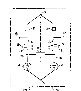
F~ ctiollal Mod~l
Figure I is a functional model of the ~ircuit ~tructure of our invention employillc
field effect transistors Our invention employing bipolar transistors is al~o depicted in Ficul~
I A wherein bipolar transistors 30' have been u~ed in pla~e of the filed effect transi~tor~ 30 ot`
20 Fi~ure 1 It is comprised of two parallel symmetric circuits 101a and ll)lb Ea-h ~ir~uit i~
~omprised of a load 20, having a resistive component, in ~erie~ with an output node 15 a
transistor 30, and a current source 40 The tran~i~tor 30 h~s three ele-trodei 31, 32 and 33 For
bipolar transi~tors, as seen in Figure IA, ele~trode 31 ' i~ known as the collector, electrode 32'
is known as the emitter, electrode 33' is known a~ the base For field effect transistors as ~een
25 in Figure 1, electrode 31 is known as the drain, ele~trode 32 is known as the sour~e, and
electrode 33 is known as the gate Our invention i~ not dependent upcin the transistor type u~ed
for transistor 30
These two circuits 101a and 101b are onne~ted at three locations node 10, node 11
30 and by a signal detector 50 connected between llodes 12a and 12b DC voltages are applied to
node~ l()and 11 toprovideacommonvolta~e(ti~`ierentiala~ro~seachparallelcircuit l()laa
I()lb Additional DC voltages are applied by ~ 13 and 14 to properly bias the tranii~tor~
30 and establish a voltage differential betwe~ two parallel cir~uit~ 101a and 101b at llod~
12aandl2b.ThevaluesoftheDCvoltage.~ap~-iic(ltollode~1(),11,13andl4aresu~hthat.i
35 ( mnhin~iinn with the parameters of the cho~ r lll~i~t(lr~ 30, the voltage differential bet~
nodes 12a and 12b is sufficient to properly bia~ icll~l detector 50
The voltages applied to the input ~lo~ . I l. 13 and 14 bias the transi~tor~ 3() ~)
-4a- 2~8~
that they operate in the linenr re~ion l~or bipolar transistors or the saturation re~lioll ~or
field-effeet transi~tors, i.e. the regions where ~hanges in volta~e do not appre~iably ~h~nce
tr~nsistor
1()
~1
WO 92/19039 "'-r/US92/00995
~ -s- 21~80~9
current. The current sources 40 maintain an equal D~ current in each
parallel circuit lOla and lOlb. The equal DC current through each parallel
circuit lOla and lOlb results in an identical voltage drop across each load 20.
Consequently, without any other external stimuli, the voltages measured at
5 output nodes lSa and lSb would be equal. However, when signal energy i~
detected at the signal detector 50, it is converted to current as input at node~12a and 12b. The current provided as input to nodes 12a and 12b increases
the current between node 10 and node 12a in circuit lOla and decreases the
current flowing from node 10 to node 12b in circuit lOlb. As a result the
10 voltage drop across load 20 in circuit lOla increases and the voltage drop
across load 20 in circuit lOlb decreases. The measured change in the output
voltage at node 15b results in a positive pulse in response to a signal pu]se
received by the signal detector from the signal transmission system. The
measured change in the output voltage at node 15a resu]ts in a negati~e
15 pulse in response to the signal pulse received. The measured voltage pulse~
at nodes 15a and 15b v~ould be equal in magnitude but 130 degrees out of
phase .
If this differential transimpedance amplifier circuit is
used within an optical receiver., the signal detector 50 would be a
20 photodetector and the signal transmission system 60 would be an optica]
transmission system. The photodetector could be a meta]-semiconductor-
metal (MSM) photodetector or a P-I-N photodiode. If a P-I-N photc~diode i~
used, it is necessary to maintain a positive bias across the detector from
circuit lOla to lOlb whereas with an MSM photodetector bias po]arit~ is not
25 important. Figure 2 depicts our invention as used within an optica] recei~er
and with a P-I-N photodiode 50'. An optical fiber 60 from a fiber optic
transmission system is terminated at and optically coup]ed to the
photodetector 50. The received optical signal results in a current input to
the differential transimpedance amplifier which, as described abo~e,
30 produces an output voltage responsive to the input.
In addition, our invention is not limited to optical
receivers. The circuit structure is applicable for any high frequenc~
receiver. The signal detector 50 could be a high-frequency energy detector,
an example of which is a millimeter wave detector, and the signa]
35 transmission system could be a microwave transmission s~stem. Fi~ure 3
depicts our invention as used within a wideband microwave recei~er. A hig~h
frequency waveguide 70 is coupled to a millimeter wave detector 50''. The
WO 92/19039 % 1 0 8 ~ PCI /US92/00995
microwave signal received results in a current input to the differential
transimpedance amplifier which, as described above, produces an output
voltage responsive to the input.
It is not necessary that each circuit 101a and 101b ha~e
5 a separate current source; instead the two current sources could be combined
into a signal current source connecting nodes 12a and 12b to node 11 as long
as the single current source maintained nearly identical D.C. currents in
circuits 101a and 101b.
Our circuit structure is not inherently frequency
10 limited. Ideally, the frequency capability should approach the frequenc~
capability of the embedded transistors 30. However, the impact of the
detector capacitance and of the interconnection parasitic capacitance does
reduce the performance of the circuit structure to a percentage belo~! that of
the unit current gain cut-off frequency of the embedded transistors. The
15 interconnection parasitics can be reduced by integrating the signa~ detector
50 and the rest of the circuit elements onto the same chip.
Specific ~:n~bodiment of ~ile Inventive Circ~il
Figure 4 is a circuit diagram of an illustrative
embodiment of our invention using field effect transistors (FET) and a
20 metal-semiconductor-metal (MSM) photodetector. To facilitate our
explanation of this specific embodiment of our invention, the same reference
numbers are used in Figure 1 and Figure 4 to identify the equivalent circuit
elements. Figure 4 shows input nodes 10, Il, 13, and 14, and output nodes
lSa and b. Transistors 30 from Figure I are shown as FETs 30a and 30b in
25 Figure 4. The two current source means 40 from Figure 1 ha-~e been
expanded in Figure 2 to show the embedded technology and are shown as
sources 40a and 40b.
FETs 30a and b are high electron mobility transistors
(HEMT) with 100 ~m channel width and 1.3 ~m length. Under a -.7 V bias
30 their unity gain cut-off frequency is 14 GH~. The MSM photodetector 50' is
a light triggered current source with a large internal impedance and a lo~
leakage current. Resistors 20a and 20b are the output loads. Current source
40a is made up of a cascode arrangement of transistors 401a and 402a v~ith a
third current path from the gate of FET 30a in circuit 101a 1O node 11. This
35 third current path is comprised of a resistor 410 in series with two diodes
412 and 413. Resistor 410 and diodes 412 and 413 are providing a -1.5 volt
,, . ., ~ : . . . . . . . .
WO 9~119039 PCl /US92/00995
2la~0~s - ,
reference bias at the gates of transistors 401a and 401b. Current source 40b
is made up of a cascode arrangement of transistors 401b and 402b.
. Transistors 401a and b and 402a and b are also FET, with transis~ors 401
having a 40 ~m channel length and transistors 402 having a 30 ~m c~annel
S width.
In this specific embodiment of our invention a positi~e
6 Volt DC source is applied to node 10 and a negative 6 Volt DC source is
applied to node 11. A negative 3 Volt DC source is applied to the gate of
FET 30b at node 14, and the gate of FET 30a is grounded via node 13.
lO However, the capabilities of transistors 401a and 401b and 402a and 402b
chosen for use within the two current source means 40a and 40b do not
provide for sufficient equalization in DC bias current in circuits lOla and
lOlb. They were chosen because their operating characteristics provide the
necessary DC voltage stability at nodes 12a and 12b. To further equalize the
15 DC bias current in loop lOla and lOlb and to isolate the output form the
input, transistors 16a and 16b have been added in a cascode arrangen1ent
between nodes 15a and 15b and FET 30a and FET 30b The gates of these
two transistors are biased by a 1.5 Volt DC voltage source.
11pon a lightwave pulse from optical fiber 60 impinging
20 on photodetector 50' the current generated by the photodetector ~ould
increase the current between node 10 and node 12a in circuit lOla and
decrease the current flowing from node 10 to node 12b in circuit lOlb. As a
result the voltage drop across resistor 20 in circuit lOla would be incIeased
and the voltage drop across resistor 20 in circuit lOlb would be decreased.
25 The measured change in the output voltage at node 15b would result in a
positive pulse in response to a lightwave pulse received. The measured
change in the output voltage at node 15a would result in a negati~e pulse in
response to the lightwave pulse received. The measured voltage pulses at
nodes 15a and 15b would be equal in magnitude but 180 degrees out of
30 phase. In this embodiment transistors 16a and 16b are HE~T with a 40 ,ILm
channel length. The operational bandwidth of this specific embodiment of
our invention is close to 65% of the unit gain cutoff frequency of FET 30a
and 30b. If transistors with sub-micron gates were used the operational
bandwidth of the circuit would be in the lO's of GHz range.
WO 92/19039 PCI`/US9Z/00995
8 --
21 ~8~19 Clearly, those skilled in the art recognize that the
principles that define our circuit structure are not limited to the embodiment
illustrated herein. Other embodiments may be readi~y devised by those
skilled in the art.