Note : Les descriptions sont présentées dans la langue officielle dans laquelle elles ont été soumises.
- 2116257
1 -
PHOTODETECTOR WITH A RESONANT CAVITY
Field of the Invention
This invention concerns photodetectors with a resonant cavity.
Back~round of the Invention
Wavelength selective detectors are useful in wavelength-division
multiplexing applications. By sending separate signals at different wavelengths
through an optical fiber, and detecting these wavelengths separately, one can
increase the information capacity of a comml~nir.ations system. The light sources
could consist of semiconductor lasers or naITow-spectrum light ernitting diodes
10 (LEDs) such as a resonant cavity LED (RCLED). The detection system must be able
to demultiplex the signal, i.e., detect the different wavelength signals separately.
Each detector in the demultiplexing scheme must be able to detect the light from its
design wavelength with good efficiency, while being insensitive to all other
wavelengths in order to minimi7e cross-talk between channels.
E~ecently, resonant cavity enhanced (RCE) photodetectors have been
studied for use in wavelength-division multiplexing applications. These designs
place the absorbing region of a photodetector within a Fabry-Perot resonant cavity
consisting of epitaxial serniconductor layers. Such devices can exhibit high speed,
can have thin absorption regions, and detect light most strongly at the resonant20 wavelength of the cavity while reflecting non-resonant wavelengths. These devices,
however, require the growth of a thick epitaxial distributed Bragg reflector (DBR)
semiconductor mirror below and usually above the active region. For example, seeK. Kishino et al., "Resonant Cavity - Enhanced (RCE) Photodetectors", IEEE
Journal of Quantum Electronics, Vol. 27, No. 8, August 1991, pages 2025-2026.
25 Summary of the Invention
Specifically, there is disclosed a resonant-cavity p-i-n photodetector
based on the reflection or transmission through a Fabry-Perot cavity incorporating
non-epitaxial, amorphous layers with alternating refractive index difference electron-
30 beam deposited on a light-gathering side of a commercially available photodetector. The
materials of the Fabry-Perot cavity are selectable from materials refractive indices
of which fall within a large range (from n=1.26 for CaF2 to n=3.5 for Si) preferably
from rnaterials which when deposited are in an amorphous state. The material
combinations are selected so that only wavelengths resonant with the cavity mode35 will be detected. The microcavity of the RC-PIN design can be deposited by
electron beam evaporation on any existing detector structure, without modification
of semiconductor growth Such a photodetectorwould be useful for wavelen~th
-2- 2116257
demultiplexing application. The ease of layer deposition, as well as the high degree
of tailorability of spectral position, spectral detection width, and maximum
numerical aperture of efficient detection, make the RC-PIN attractive for use inwavelength demultiplexing applications. An exemplary RC-PIN photodetector
5 includes a Si/SiO2 Fabry-Perot cavity electron-beam deposited on the InP substrate
of a commercial InGAs photodetector. The detection efficiency relative to a
reference device was 52 percent at the resonant wavelength of 1350 nm, with a
resonance width of 14 nm, and a 4 percent response for off-resonance wavelengths in
the 1 100-1700 nm range.
In its broad scope the invention consists of a photodetectorwhich
comprises a photodiode comprising a substrate, a light-absorbing region and electrodes to
the substrate and the light-absorbing region, said photodiode having a light-collecting
surface, in which a Fabry-Perot cavity is formed upon said light-collecting surface, said
Fabry-Perot cavity including, in an ascending order from said light-collecting surface, a
15 distributed Bragg reflector (DBR) bottom mirror, an active region and a DBR top mirror,
each of said top and bottom mirrors comprises a plurality of periods, each period
comprising a layer of a material with higher refractive index and a layer of a material
with lower refractive index than the other layer in the period, a layer with higher
refractive index in one period being adjacent to a layer with lower refractive index in
another period of the mirror, each of said layers in the DBR mirrors being ~/4 thick, said
active region having a refractive index which is different from the refractive index of
each adjacent layer in the periods adjoining the light absorbing region, said active region
being ~/2 thick.
The invention also consists of a method of fabricating a photodetector
with a Fabry-Perot cavity on a light-collecting surface of a photodiode comprising a
substrate, a light-absorbing region and electrodes to the substrate and the light-absorbing
region, which comprises depositing on the light-collecting surface of said photodiode a
plurality of alternating layers of a material with a low refractive index and of a material
with a high refractive index so as to form a DBR bottom mirror on the light-collecting
surface, an active layer on the DBR bottom layer, and a DBR top mirror on said active
layer.
- 2116257
-2a-
Brief Description of the Drawings
FIG. 1 is a schematic representation of a structure of a Fabry-Perot
resonant microcavity formed on the light collecting surface of a standard p-i-n
photodetector;
FIG. 2 is a plot of the reflection spectrum of a test wafer with a
Fabry-Perot microcavity grown at the same time as the one on the photodetector;
FIG. 3 is a plot of the detected photocurrent from a resonant cavity
p-i-n (RC-PIN) photodetectorwith a deposited Fabry-Perot cavity, divided by the
photocurrent from a reference detector with an anti-reflection coating but no cavity; and
l O FIG. 4 is a series of plots of a maximum relative response of the
Fabry-Perot cavity of the RC-PIN photodetector for various fractional resonance widths
(t) versus the numerical aperture of the incoming light divided by the effective refractive
index of the cavity NA/nc.
Detailed Description
This invention embodies a wavelength-selective photodetector which
consists of a p-i-n semiconductor structure and an adjacent resonant optical
microcavity formed by an active region and a pair of DBR mirrors. The cavity canconsist of a variety of transmitting material combinations which may be deposited by
a number of deposition techniques. The material combinations are selected so that
only wavelengths resonant with the cavity mode will be detected.
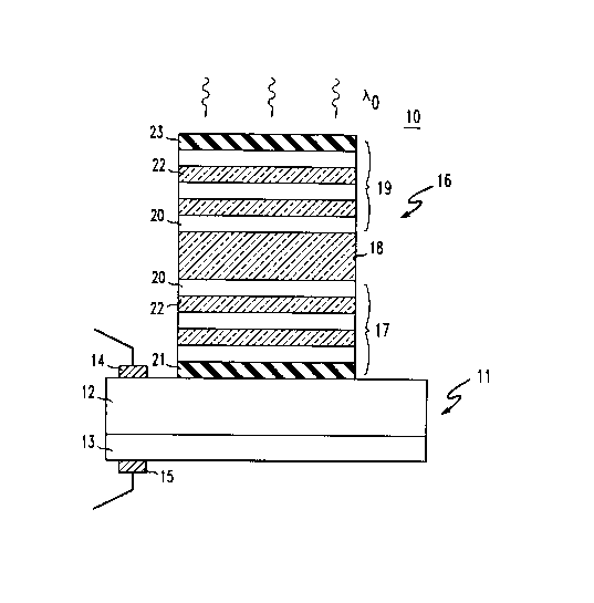
The RC-PIN photodetector, 10, embodying the invention is
schematically represented in FIG. 1 of the drawings. For illustration purposes,
various dimensions of the device are not shown to scale. Photodetector 10 includes a
photodetector structure, 1 l, including a semiconductor substrate 12, an absorbing
region 13, and electrodes, 14 and 15, to the substrate and to the absorbing region,
respectively. Photodetector 10 further includes a microcavity, 16, grown upon
21162~7
- 3 -
substrate 12. The microcavity includes a bottom distributed Bragg reflector (DBR)
mirror, 17, an active region, 18, and a top DBR mirror, 19.
The DBR mirrors each include a plurality of pairs of layers, each layer
being ~4 thick, one layer in each pair having an index of refraction dirr~,lcl~ from
5 the index of refraction of another layer in the pair. The material of each layer, their
respective index of refraction, and the number of pairs (or periods) of layers are
being preselected to provide a desired reflectivity to each mirror, so as to induce the
passage of optical radiation impinging on the top layer of the top mirror to pass onto
and into the substrate of the photodetector.
This invention is described with reference to a microcavity formed by a
sequence of layers of low and high refractive index, with active region 18 being of a
low refractive index and adjacent layers 20 being high refractive index layers of the
bottom and top DBR layers. Preferably these materials are selected from materials
which, when deposited, are in an amorphous state. Use of electron beam evaporation
15 permits a simple way of depositing such materials. In the specific example, the
material with the high refractive index is Si (n~3.5) and the m~ten~l with the low
refractive index is SiO2 (n~1.46). A layer, 21, adjacent the substrate is a low
refractive index material, SiN x, deposited as an antireflection coating on the
substrate. SiNX layer is then followed by an ~lte~n~ive sequence of electron beam
20 evaporated Si and SiO2 layers 20 and 22, respectively, such that SiO2 active layer
18 is bounded by Si layers 20. The uppermost layer 23 in the top DBR is a low
refractive layer different from SiO2. In this example, this layer is Al2O3 (n~ 1.64).
This low refractive index adjoins an air layer (another low refractive index material).
While this does not conform to the rule of ~ltt~nn~ting layer of high and low
25 refractive indices, this is acceptable in order to have a match between the top and
bottom reflectivities of the system.
In an exemplary embodiment of the invention RC-PIN photodetector 10
includes a co~ ;ial p-i-n InGaAs photodiode 11 grown upon an InP substrate 12
with the light being collected through the substrate. Surface collection is also30 possible with the present RC-PIN photodetector design. After a ~/4 thick SiN x layer
is formed on the substrate by deposition, the rest of microcavity 16 is grown upon
substrate 12 by electron beam evaporation of bottom DBR mirror 17, active region18 and top DBR mirror 19 at a substrate len-pel~lure of 100 C. Bottom DBR mirror
17 is formed by deposition on the SiN,~ layer of an alternating succession of ~J4
35 thick Si (965 nm thick) and SiO2 (1155 nm thick) layers ending with the Si layer.
Next a SiO2 active layer 18 was deposited in a thickness corresponding to
21162~7
-- 4 --
~12=(2310 nm). This was followed by deposition upon the central semiconductor
region of another sequence of alternating ~14 thick Si and SiO2 layers forming top
DBR mirror 18. The final layer of the top DBR mirror is a ~14 thick Al2O3 layer,23, deposited on top of the uppermost high refractive layer (Si) of the top DBR
5 mirror to tune reflectivity of the top mirror for maximum tr~n~mis~ion at the
resonance vacuum wavelength ~O of 1350 nm. In the specific example the bottom
DBR mirror was formed with 3 periods of low and high index layers, one of which
included the SiN x layer. The top DBR mirror was formed also with 3 periods, oneof which included the Al 2 03 layer.
While this specific example is presented using Si and SiO2 as the high
and low refractive index materials, the materials may be selected from such highrefractive index materials as Sitn~3.5), GaP (n~3.5), ZnS (n~2.3), TiO2 (n~2.2),SiNX (n-l.9), cubic zirconia (n~l.9), and such low refractive index materials asTiO2 (n~2.2), SiNx (n~l.9), cubic zirconia (n~l.9), Al2O3 (n-1.64), titanium silica
glass (n-1.54), phosphor silica glass (n-1.5), borosilicate glass (n-1.46), SiO2(n~1.46), MgF2 (n~1.38) and CaF2 (n~1.3). In some instances m~t~ of the low
refractive index group having higher index of refraction, e.g. cubic zirconia (n=1.9)
or TiO 2 (n~2.2) may be used in combination with such lower index of refraction as
e.g. CaF2 (n~1.3), MgF2 (n~1.38), borosilicate glass (n~1.46).
The cavity will be at resonance, and will transmit light if the following
resonance condition is met:
+~ + 4~1nactLact 2 I (1)
~o
wherein l~PRl and q)R2 are the reflection phases at the interfaces between the active
layer and the bottom and top DBR mirrors, respectively, nact is the refractive index
25 of the active layer, and LaCt is the thicknçss of the active layer. For ~o=1350 nm,
~t) Rl =7~ and q~ R2=7~ and L act =~n/(2n act) = ~/2, Dirrerent thicknesses for the DBR
constituent layers or for the active layer or both, will shift the design wavelength.
For active layer thicknesses greater than ~, two or more resonance wavelengths will
exist within the high reflectivity region of the DBR mirrors.
The reflection spectrum of a reference wafer with the microcavity
thereon is shown in FIG. 2. A high reflectivity region extends from 1000 nm to 1800
nm, with a reflection dip 15 nm wide at the cavity resonance of 1350 nm,
corresponding to the tran~mi~sion resonance of the microcavity. The reflection dip
drops to 10 percent and has a width of 10 nm (8 meV). By fine tuning the top mirror
35 reflectivity, the reflection on resonance can theoretically be reduced to zero. The
2116257
spectral width of the reflectance dip ~0 at wavelength position ~0 is given by:
~,~ o ~ 1-~ (2)
~ 2LCav ~4~
wherein R 1 and R2 are top and bottom mirror reflectivitiest respectively, and LCav
is the effective cavity length. The effective cavity length LCav is a multiple of the
5 wavelength of light, ~, within the cavity. For structures resulting from a 0.5 ~ thick
central SiO 2 region and a 0.2 ~ effective penetration depth into each DBR mirror,
LCav ~ 0.9 ~. This LCav is much shorter than the values obtainable in a
semiconductor RCE detector, which are typically greater than 2.5 ~ because of much
greater mirror penetration depth. The smaller L Cav and large spectrum of high
10 reflectance in this RC-PIN device is due to the large refractive index di~erellce
between the Si layers (n z 3.5) and the SiO2 layers (n z 1.46) in the DBR. The
theoretical mirror reflectivities are about 0.96, which gives a theoretical width of
about 11 nm, which is close to what is observed. By selecting materials for the
mirror layers from a large variety of materials with a wide range of refractive
15 indices, the spectral width and reflectance width can be tailored independently of the
total mirror reflectivity.
A lossless microcavity filter transmits 100 percent of the light on
resonance if the top and bottom DBR mirrors are of equal reflectivities, or R 1 = R 2
Similar mirror reflectivity constraints are also seen in resonant cavity enhanced
20 (RCE) photodetectors. For a RCE photodetector, with an active medium with
single-pass tr~n~mission T (including any ~ntino~e effects), the detection efficiency
is a maximum only when R 1 = R2 T2, with a value of 100 percent only if R2 = 1.
The equal mirror reflectivity constraint of the microcavity of the RC-PIN
photodetector is certainly easier to realize than the dual constraints needed in a RCE
25 detector. In both types of optimized devices, the maximum theoretical contrast ratio
between on resonance detection, and off-resonance detection is given by (l+R2)/(l-
Rl)2.
The response of a detector with cavity versus wavelength, relative to adetector with anti-reflective coating, is given in FIG. 3. The figure illustrates that
30 light is detected only at the resonance wavelength of 1350 nm, whereas the detector
is insensitive to all other wavelengths. The detection is low from 1100 nm to 1800
nm except for the 14 nm wide resonance at 1350 nm where the relative detection is
50 percent. The reflected light can, in principle, be detected by other RC-PIN
photodetectors, con~tinlting a wavelength-division multiplexing system. The
2116257
maximum relative responsivity at 1350 nm wavelength is 52 percent while the
response off resonance is about 4 percent. The discrepancy between the 10 percent
reflection and the 52 percent response can theoretically be explained by an .
absorption coefficient of 150cm- 1 in the amorphous silicon. Growth at higher
5 temperatures, or by CVD deposition can produce silicon layers with reduced
absorption, and therefore greater detection efficiency. Other high index materials,
such as TiO2, can be substituted with no absorption loss, but with a lesser
wavelength range of suppression. Other possible sources of efficiency loss are light
sc~ttering in the films, or a slightly bumpy substrate surface resulting in a smearing
10 of the microcavity tr~nsmi~sion peak. The off-resonance response of 4 percent is
higher than the calculated 0.1 percent for a perfect layer structure with mirrorreflectivities of 96 percent. This can be due to scattered light~ either from the
surrounding detector mount, or within the layers themselves, or from the far side of
the detector. Any reflections from the far side of detector, whether specular or15 diffuse, will reduce the detected signal on resonance, and increase it off resonance.
The resonance wavelength is relatively insensitive to small deviations of
incidence angle from the normal, but shifts quickly at higher angles. The resonance
wavelength versus incidence angle 00 is given by:
~res(~O) = ~rocos(sin-l(sin(~o)lnc)) (3)
20 The value n c is an effective index of refraction for the microcavity, which can be
determined by fitting this formula to measured or calculated shifts with angle. For
the exemplary RC-PIN devices n c is approximately 1.75. The range of angles of amonochromatic incoming light beam should be restricted such that all of the rays are
within the resonance peak. Devices with thin resonance peaks or with low nc
25 therefore require more cl llim~te l input beams for maximum detection efficiency.
For the RC-PIN detector structure, the resonance width is 14 nm at a wavelength of
1350 nm. The maximum coupling efficiencies for ideal-wavelength monochromatic
light L~ through (or ~etected by) a cavity with an effective index n c, from a
light cone of nllm~ric~l ape~ c NA = sin(00 ma~ for various fractional linewidths,
30 t= ~0/~0, is given by the following formula:
tan~l 1 -cos(sin-l (NA/nc))
t
Max.EfficienCy(NAlnc) = l-cos(sin 1 (NA/nc)) (4)
The calculation ~is~lme a uniform intensity of light over all solid angles within the
light cone, and includes only the effect of resonance shift with angle, assuming no
2116257
- 7 -
change in the peak detection efficiency with angle. A graph of efficiency relative to
a parallel beam for various fractional linewidths is given in FIG. 4. One can see that
for the device with t = 0.01, and nc = 1.75, the relative coupling efficiency for a light
cone with NA < 0.29 is greater than 0.69, and for NA < 0.20 is greater than 0.89.
An incident beam, with rays experiencing resonance wavelength shifts
up to the value of the resonance width, results in relative efficiency of 78.5 percent.
For larger N A values, the relative efficiency drops rapidly. A microcavity should
therefore be designed to have a relative efficiency larger than 78.5 percent for the
given N A of the light source. The exemplary cavity meets this criterion for
10 nllm~ric~l aperture values of less than 0.25. Larger NA values can be achieved by
designing a slightly wider spectral width, or a similar spectral width and a larger n c .
The cavity index nc can be increased by replacing the central SiO2 region, or even
all SiO2 layers, by a higher index material.
It is also possible to create an equivalent cavity with combination in
15 which the active layer with a high refractive index is bounded by DBR mirrors with
low index m~teri~l being adjacent to the active layer. An illlpol~lt prerequisite
would be the ability of the middle layer to be highly transparent to optical radiation.
Additional advantages and mo~lifi~tions will readily occur to those
skilled in the art. Therefore, the invention in its broader aspects is not limited to the
20 specific details, l~;pl~sentative devices, and illustrated examples shown anddescribed. Accordingly, various moflifications may be made without departing from
the spirit or scope of the general inventive concept as defined by the appended claims
and their equivalents.