Note : Les descriptions sont présentées dans la langue officielle dans laquelle elles ont été soumises.
CA 02119862 2000-03-15
-1-
Battery Voltage Measurement System
Technical Field
This invention relates generally to measurements of
battery power supplies, and particularly to a temperature
stable system for accurately measuring the voltage of
individual battery modules making up a battery power
supply.
Background Art
There are many instances in which battery cells, or
battery modules, are serially connected in a bank or banks
to provide a higher voltage than otherwise available.
Unfortunately, th~~ condition of the bank of cells as a
whole is dependent: upon the condition of individual cells
or modules, and it is well known that in order to detect
and locate a deteriorating one of these, individual
measurements must be made at the cell or module level. As
an example, where there is a bank voltage of 126 volts, it
might be in the form of ten 12.6-volt lead acid
batteries. In such case, condition measurements would
typically require that each individual 12-volt battery be
subject to measurement, which would necessitate the wiring
harness extending from each battery back to the point of
instrumentation making the measurement, and wherein there
would be a wire :Eor each terminal, or, in this case, a
total of 11 wire:c. This has been regarded as quite
cumbersome.
Accordingl~~, applicant has previously devised a
battery voltage measurement system having a plurality of
bi-level switchincl circuits each forming a switch that
closes at a discrete voltage level and opens at a set,
slightly higher potential. One terminal of each of these
switches is connected i~o a common lead, and the other
terminal of these switches is connected to one of the
positive-to-negative connections between
:;:.. . . ', ,., . . . . . ..
WO 93/06473 PGT/US91/07018
the discrete battery cells making up the bank of
batteries. Thus, each positive-to-negative battery
connection is also coupled in parallel to the common
lead via the bi-level switches. A ramp voltage is
generated and applied between the common lead and the
battery bank, sequentially causing the bi-level ,
switches to first close and then open, sequentially
generating a current pulse from each battery. The
ramp voltage and current pulses through this circuit
is concurrently measured and displayed wherein the
difference in voltage between the current pulses, with
the first pulse utilized as a reference. ~is
illustrative of the battery voltage of the individual
battery cells making up the bank of batteries.
While this scheme works relatively well, problems
have become apparent. Notably, in each of the bi-
level switch circuits, a diode passes the current
generated by the difference in ramp voltage and
battery voltage. This diode has proved to have
instabilities related to temperature. which in turn
causes inaccurate measurements of battery voltage.
Further, the design -of the circuitry of the bi-level
switches includes a field effect transistor (FET) that
is utilized to switch the current, with this FET
controlled by a NPN transistor. This transistor and
FET are also subject to temperature instabilities and
noise, such as noise generated by battery charging
eguipment, that causes nonlinear responses from the
FET and transistor.
In accordance with the foregoing, is an ob3ect of
this invention to provide an improved battery voltage
measurement system which is insensitive to temperature
gradients between discrete bi-level switches of the '
invention, has better response than the circuitry of
prior art, and is insensitive to noise generated by
switching circuitry in battery charging networks.
..
w . .. . ... ~., , :., ..
WO 93/06473 PGT/US91/07018
- 3 -
211~8~2
Disclosure of Invention
. .
In accordance with this invention, one connection
of a plurality of voltage responsive switches is
coupled to intermediate terminals of a bank of battery
modules, one switch per intermediate terminal. The
other connection of the switches is coupled to a
common terminal. A ramp voltage is applied between
r;:, . the common terminal and the battery module, this ramp
'' voltage being such as to extend from below a voltage
s' of one of the batteries to dust in excess of the total
10. voltage of the bank of batteries. As the voltage is
"r
tamped up, the switches are sequentially closed and
opened, giving rise to current pulses. Both the ramp
voltage and instantaneous current through this
arrangement are coordinately provided as outputs.
wherein the voltage between discrete current pulses
are used to determine battery condition.
Brief Description of the Drawings
Fig. 1 is a block diagram of an embodiment of the
invention.
.Fig. 2 is a schematic diagram of one of the
switches employed in the system and provided with
integral temperature compensating circuitry.
FiQ. 3 .is an oscillographic display of current
versus voltage, particularly illustrating the
operation of the system.
Best Mode For Caking Out the Invention
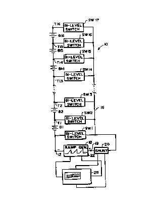
Referring to Fig. i: there is shown a battery
assembly l0 consisting of a plurality of six-volt
battery modules designated 81-816, only seven of
which are shown, with battery assembly 10 producing a
nominal voltage of about 96 volts. The negative
terminal of battery module Bl is connected to terminal
12, and the positive terminal of battery module 816 is
connected to terminal '":6, the intermediate batteries
being connected in series by connecting terminals
. ~ ..~... ,. ','
,' ~ . . ' , . . '.
.~ ~ ~
;
.
.
.
WO 93/06473
PGT/US91/07018
~ 211986
s
- 4 -
_
designated T1-T15, only T1-T2 and TI3-T15 being shown.
Of course. the battery voltage at each of terminals
T1-T15 is derived by the number of battery connections
below a particular connection, with 6 volts on
terminal T1, 12 volts on terminal T2, and so on to
terminal 14, where the entire battery assembly voltage .
of 96 volts is felt. Two-threshold, or bi-level,
switches SW1-SWI? are employed wherein one terminal of
each switch is connected to common lead or terminal
16, and the opposite lead of each is connected to one
of terminals i2, TI-T16. These switches are
at
identically set to close at a like discrete voltage
their terminals and to open at a slightly higher
potential. The first bi-level switch SWI is coupled
between the negative terminal 12 of battery assembly
10 and common terminal 16, and is used as a reference.
Ramp voltage generator 18 and current sensing
shunt 20 are connected in series between negative
terminal 12 and common terminal 16. Ramp voltage
generator 18 generates a ramp voltage waveform 22
which commences at zero volts and rises to about 100
volts, approximately 4 volts above the nominal voltage
of 96 volts of battery assembly 10. Current shunt 20
provides a voltage representative of current flow
through switches SW1-SWiT. The ramp voltage from ramp
voltage generator 18 is provided to the horizontal
input of an oscilloscope 28, with the voltage output
from current sensing shunt 20 provided to the vertical
input of oscilloscope 28. As the ramp voltage rises
on terminal 16, it sequentially rises above the
voltage appearing at each terminal T1-T15 and finally
just above that on terminal T16, sequentially closing
'
_~ and then opening each of switches SW1-SW1?, generating
a series of current. pulses. The ramp voltage is also
f:~;
applied as an X axis or horizontal sweep voltage tc
oscilloscope 28, and the voltage output of current
i~ measuring shunt 20 is connected to the Y or vertica:
a
axis input of oscilloscope 28.
WO 93/06473 PCT/US91l07018
.. _ 5 -
.. 21198(i~
Fig. 2 shows a schematic circuit diagram of one ~~
of the switches which is generally labelled a bi-level
switch SW (Fig. 1). Switch SW is voltage responsive
as described across its terminals to close and pass
current when its right terminal is more positive than
its left by about 2 volts and to open and block
current flow when this voltage difference rises to
approximately 2.5 volts. Thus, as the bi-level
switches are sequentially opened and closed by the
rising ramp voltage, a waveform appears on
oscilloscope 28 comprising a series of current peaks,
the first peak P1 representative of a current pulse
through switch SW1, peak P2 representative of current
flow through switch SW2, and so forth to peak i?. In
the instance where discrete battery cells each
contribute a like potential to the total potential, in
this example, six volts, each peak will be slightly
higher than a preceding peak, with the peaks
approximately equally spaced as shown in Fig. 3, the
spacing between the peaks corresponding to the
difference of potential between discrete battery
cells. In the instance where a battery is in marginal
condition and is contributing a lower voltage, the
particular switch SW associated with the marginal
battery closes at a lower potential, displacing the
current peak for that battery to the left, as shown by
peak PS, conveniently identifying marginal battery B4
for replacement. The correlation between a displaced
current pulse and a marginal battery cell may be made
by direct observation~of an oscilloscope, or in a
computerized system, by software disposed for directly
indicating the marginalbattery.
Examining now one of switches SW, illustrated in
Fig. 2, the operative current path there through for
generating one of the current peaks shown in Fig. 3 is
through zener diode 30, N-channel, enhancement mode
field effect transistor (FET) 32, N-channel.
enhancement mode FET 33, and current limiting resistor
WO 93/06473 PGT/US91/07018
- 6 -
i
34, with these components generally coupled in series
to provide a limited current flow of about 10
milliamps through switch SW. FETs 32 and 33 are
selected to conduct when the gate terminals thereof
are more positive than the drain terminals by about
~
to the .
1.5 volts. Two FETs are used here due
selection of FETs used in this circuit, which FETs
have a slight unidirectional leakage current from
source to drain when biased "off." Thus, FET 32,
positioned drain-to-source with respect to FET 33,
blocks this leakage current and prevents the- leakage
current from affecting voltage measurements. However,
it is possible that FET 32 may be omitted with
selection of a different FET for FET 33.
The cathode of zener diode 30, which is selected
to conduct at about 2.0 volts, is connected to
terminal 16 and receives the ramp voltage, with the
anode of diode 30 coupled to the source terminal S of
FET 32. The drain terminal D of FET 32 is coupled to
the drain terminal D of FET 33, in turn having its
source terminal S coupled via current limiting
resistor 34 to the left-hand terminal of switch SW,
which receives a potential from bank i0 determined by
the number of battery connections below it. Gate G of
FET 33 is coupled as shown via high impedance
resistors 40 and 41 of filter circuit 38 to terminal
l6 and to the collector of NPN transistor 35. The
Qate terminal G of FET 32 is coupled directly to
terminal 16. Thus, FET 33 is biased "on," with
transistor 35 in the"off" state, when the ramp
voltage applied via resistors 40 and 4i to gate G of
FET 33 rises to about 1.5 volts above the battery
voltage applied to the drain of FET 33: Likewise, as
the ramp voltage rises about 1.5 volts above the
battery potential, FET 32 is also biased "on" by
virtue of the battery potential being felt at drain D
thereof via resistors 34 , 36 and 3? and gate G being
coupled directly to the rising ramp voltage applied to
CA 02119862 2000-03-15
_7_
terminal 16. As the rising ramp voltage reaches about 2.0
volts, zener diode 30 conducts, permitting current flow
through diode 30 and FE;Ts 32 and 33. Thus, in contrast to
applicant's prior system, the FETs are biased "on" prior
to conduction of diode 30, meaning that any variation in
the voltage potential at which the FETs are biased "on" is
not passed to current sensing shunt 20 and oscilloscope
29. Further, since diode 30 is a very temperature stable
device, temperature differences that may be present
between discrete switches SW in a battery bank have no
effect upon the two-volt threshold of these switches,
allowing reliable voltage and current measurements of each
battery cell to bE~ taken.
Control of the FETs is effected by a voltage
sensing circuit including transistor 35 and resistors 34,
36 and 37, with tnansis~tor 35 having an emitter coupled to
the left-hand terminal of switch SW, a collector coupled
through a filter circuit 38 comprised of high impedance
resistors 40, 41 and capacitor 42 to terminal 18 and to
the gate input G of FET 33, and a base coupled via
resistor 36 to tile source terminal S of FET 33 and via
resistor 37 to the drain terminal D of FETs 32 and 33.
Resistors 34 and 36 form a voltage divider network that
proportions the voltage drop across resistor 34 such that
about 700 millivolts is. applied to the base of transistor
35 when the ramp voltacte rises to about 2.5 volts above
the battery voltage. Coupled as such, increasing current
flow through FETs 32 and 33 due to increasing ramp voltage
causes an increasing voltage drop across resistor 34, with
this voltage drop proportioned by resistor 36 and applied
to the base of t~_ansistor 35 via resistor 36. When the
voltage applied to the base reaches about 700 millivolts,
corresponding to a ramp voltage difference between the
battery voltage of about 2.5 volts, transistor 35 is
biased "on" with the rE:sult that the slightly higher ramp
voltage is
WO 93/06473 PGTlUS91l07018
_ g _
shunted to the battery potential, equalizing the
potential between drain D and gate G of FET 33,
biasing FET 33 "off" and blocking further current flow
through bi-level switch SW. After transistor 35 is
biased "on," it is latched "on" by a small current
flow through resistor 3? and resistor 34, which form a
second voltage divider network that proportions a 2.5-
volt difference between the ramp voltage and the
battery voltage to apply about T00 millivolts to the
base of transistor 35. This in turn keeps FET 33 off,
blocking current flow through switch SW. ~ When the
ramp voltage reaches its peak and falls back to about
0 volts, the voltage applied to the base of transistor
35 disappears and transistor 35 reverts back to an
"off" state, decoupling gate G from drain D of FET 33
in preparation for the next ramp cycle. A second
zener diode 39, selected to conduct at about 10 volts,
is coupled between the gate G and source S terminals
of FET 33, and serves to protect FET 33 from an
overvoltage condition between source and drain
terminals occurring when the ramp voltage falls to
zero volts. Filter circuit 38 functions to block
noise, such as switching noise from charging
equipment, when transistor 35 is switched "on."
Initially, the operation of switch SW1 (Fig. 1
will be considered, with ramp generator 18 just
startiaQ its rise from zero voltage. When the ramp
voltsQe applied to terminal 16 rises to just above
approxiaately ?.5~ volts, 1.5 volts above the battery
voltage felt at the left-hand terminal of switch SW1,
FETs 32 and 33 arc biased "on" as described. Further
increase of the ramp vo:tage to about 8.0 volts causes
diode 30 to conduct, a:lowing current to flow through
PETS 32 and 33, diode 30 and through resistor 34,
generating the leading edge of fit,st peak P1 of Fig.
3. As the ramp voltage continues to increase to about
8.5 volts, 2:5 volts above the battery voltage, the
voltage drop across resistor 34 increases directly
WO 93/06473 PGT/US91/07018
- 9 - 211862
with the ramp voltage to apply an increasing voltage
to the base of transistor 35, lowering the resistance
of transistor 35 as the ramp voltage increases and
shutting "off" FET 33, generating the falling edge of
peak P1 and latching transistor 35 "on." At about ?00
millivolts, transistor 35 is saturated, which
equalizes the ramp potential applied to gate G of FET
33 as described. biasing FET 33 completely "off" and
blocking current flow through bi-level switch SW for
the remainder of the ramp cycle. During the
conductive period of switch SW1, there will be no
current flow through switches SW2-SW1? as diode 30~of
these switches will be blocked by virtue of the
battery voltages on terminals T1-T16 being higher
than the voltage on common terminal or lead 16. After
switch SW1 opens, and as the ramp voltage continues to
rise, the switching action just described for SW1 will
sequentially repeat in the balance of the switches,
that is, switches SW2-SW1?, giving rise to the
succeeding current pulses shown in Fig. 3.
Significantly, if one reads the voltage from Fig. 3
from. succeeding on otherwise identical points on the
current pulse waveforms, the voltage difference will
be indicative of the voltage of the particular battery
module between which succeeding switches have been
operated to create the current pulses.
It is to be noted that the base point for the
current pulses gradually rises on the display of Fig.
3, this occurring by virtue of there being increased
current flow with increasing ramp voltage as more of
diodes 30 of the switches conduct. Where module
voltages are simply determined by visual examination
of the display, such as shown in Fig. 3, this poses no
point of error; whereas, where battery module voltage
is determined from amplitude points on the trailing or
leading edges of the pulses, appropriate compensation
would be provided to comparators making such an
examination either by hardware or via software.
WO 93/06473 PGT/U591/07018
- io -
119$62 From the foregoin , it is to -be a reciated that /
9 PP
applicant's system provides an improved, temperature
compensated means of battery module analysis. No
contact-type switching systems are needed, and wire
connections from the environs of the batteries to any
remotely located measurement system need only total
two wires.