Note : Les descriptions sont présentées dans la langue officielle dans laquelle elles ont été soumises.
2 :l 2 ~
- , .
...
,
"ZERO Bl~ (IURRENT L~W-SII)E DRIV~R ('ONTROL CIR(IIJrT"
....
E;CHN I CAL F'I ELr~
~:
;~ 5The present invention relates to output power stages
; employing a power switch for connecting to a ground
node a load and wherein static power consumption within
the driving circuit is substantially eliminated.
10BACKGROUND OF THE INVEIJTI ON
'';
A circuit for switchingly connecting to ground (low-
.,
side driver) an external load employing a power switch
has a basic diagram as shown in Fig. 1.
.~! 15 Commonly the power switch Pw is a transistor and
oftsn an integrated DMOS transistor that notably offers
:.
definite advantages over a bipolar junctic)n transistor.
The integrated transistor structure intrin;ical]y con-
~ tains a junction (diode) Dr through which, in case c,f
.:2, 20 reactive loads, transient currents may recirculate. The
power transistor Pw constitutes the output stage and is
controlled by a driving circuit which determines a
s,state of conduction or of nonconduction of the tran-
~,1sistor, according to a certain "duty cycle" (in most
'525 applications).
'''~2In this way, an output signal having an amplitude
''2comprised between Vl=Rdson*Id and Vh=H.V. is produced,
where H.V. is the supply voltage to which the external
load is connected, Rdson is the saturation resistance
j30 Of the power transistor Pw and Id is the current
,~, .
through the load.
In order to ensure a low voltage drop through the
~;power transistor Pw when it is cc>nclucting, and there-
,~fore a low power dissipation, it is necessary to mini-
miæe the Rclson value. This is achieved by driving the
~`,power transistor with a (gate) voltage that is higher
:,~
,,,,~,
.,~)o
~;; 2~20~8l!1
'~'
~,,
;i,tharl the voltaye that is necessary for switching-oll the
transistor. Normally, ror a DMOS transistor such an
overdrive voltage may reach about 10V, i.e. Vgs=10~',
~, ~
.that is it may be equal to the supply voltage Vcc of
~`5 the control circuit.
.;.,
h,` ~` Moreover, the output signal (OUT) is often re~uired
, .:
to have certain slew-rate characteristics (Tf and Tr)
and delays (Tphl and Tplh), as referred to the control
signal (IN), controlled and equal to each other, as
~10 depicted in Fig. 2.
;~On the other hand, in order to switch-on the power
`;transistor Pw, it is necessary to charge the ca-
pacitance of the driving node (gate node) up to a volt-
1. ,,~....
age that is higher than the threshold voltage Vth of
~i15 the transistor. If, during a switch-on phase, driving
is effected through a constant current generator Il
.~;(Fig. 1), the gate voltage will have a d:iagram versus
~'time as the one depicted in ~ig. 3. Three different
zolles of operatic)l-l of the power transistor ~lla~ he
distinguislled, as determined by the actual input
~;capacitance that varies from zone to zone.
In a first zone I of the characteristic, the gate
voltaye rises from Vgs=0V to Vgs=Vth. In this interval
of time no current flows through the power transistor
which remains in an off condition. The interval tO-tl
~iis defined as turn-on delay time. After the instant tl,
~the power transistor starts to conduct and the voltage
;,~Vds across the power transistor drops from Vh to Vdson.
.~In a zone II of the characteristic, nor~ally re-
ferred to as the saturation zone, the ratio ~ Vds/~ Vgs
`~is high and therefore the Miller effect becomes
preponderant in determining the input capacitance as
compared with the "physical" gate capacitance of the
power transistor. Because of this, the driving current
primarily charges the "Miller" capacitance while a
negligeable portion of it charges the Cgs capacitance
. ,
....
~` 2
~; .
l j:.. ~,,: : ::., --. : --
.,
.
,,
2 ~ 2 ~
...
.~
between gate and source of the power transisl(-r Pw,
thus causing a negligeable variation of the Vg.s
voltage. In fact, the gate voltage rises from the value
~- Vgs=Vth to the value Vgs=Vs (Vs is also referred to as
the operative voltage). The interval tl-t2 is defined
as the fall time Tf.
: -.
In the zone II of operation, the gate capacitance
charges completely to the voltage Vcc and the power
transistor is fully on (low internal resistance).
10Similarly, for switching-off the power transistor
,~
-~ Pw, its gate capacitance is discharged through a
constant current generator I2, which is functionally
connected between the gate node of the power transistor
and ground. During a "time off" phase phenomena similar
to those that occur during the "turn-on" phase takes
place, as depicted in Fig. 4. Also in this phase of
, ~ . i
operation in fact, the gate capacitance discharges
~:1 through three distinct phases.
In a first phase or zone I of the charactetistic,
~:i20 the gate voltage drops from the value Vgs=Vcc to the
operative voltage Vgs=Vs, while the drain voltage
. ",. .~
~remains at Vdson. This interval is defined as the turn-
;.. ~ .
: 'foff delay time.
~In a second region II of the characteristic, the
i, . .,~,, .
,,i;25 voltage Vgs drops from Vs to the threshold voltage Vth
and during this phase the power transistor Pw starts to
carry less and ~ess current until it switches-off
completely. The duration of this interval during which
`the drain voltage rises from Vl to Vh, is defined as
,;30 the rise time Tr.
,1
If the currents Il and I2 have the same value, the
rise time and the fall time are identical.
~-In order to have a large charge current (Ic) and a
large discharge current (Is) of the ga-te capacitance of
''~5~ 35 the power transistor Pw for achieving fast switching
times, while employing control current generators ll
' .'.!,.
:'.',~
!. ' ~ 3
"..,:,~,,
.~,....
: `''
i ` 2 ~ 8 ~
. .
~.
. and I2 of re]a~ively ]ow va]lle, a dri~~ing circlllt ~IS
the one depited i.rl F:ig. 5 is emp~oyed. In tact:, ti~e
,,
.. relat:ionshi.E- tllat ties the currents Ic and Is to tlle
currents ID1 and ID4 is of an expc-nential ~ind:
,,~ .,,
Ic=n*ID1 e RIM~t
-,
: . ..
','!''~ Is=n*IM e RID4~t
,;. ~;.
;i 10 If ID1 and I~ are equal, the currents Ic and Is will
~,, be equal and so also the fall time and the rise time.
In practice, in a circuit as the one depicted in
; . .,
Fig. 5, the current I~ is different from ID1. In fact,
the MOS M1 and M2 operate with a constant Vgs,
.;jr15 therefore the current ID1=I, while the MOS M3 and M9
operates with a Vgs that varies because their source is
not connected to a fixed voltage, but to the gate c,f
the power transisthr Pw, the vo]tage c-f wll:ich drc)ps
during a turn-off phase. Therefore, IDg~I.
Commonly, in order to obviate to this drawback, the
sources of M3 and M4 are connected to a fixed voltage
~f'
~-~ for example to the supply voltage Vcc, so that, the cur-
rent mirror formed by M3-M4, generates the same current
as the current mirror M1-M2. Such a knonw solution is
depicted in Fig. 6, and a functional block diagram may
be depicted as in Fig. 7.
~,,i In this circuit, the transistors M2 and M4 do not
exactly operate undsr the same conditions. In fact,
tj~ Mg operates always in a saturation zone, with
Vgsl=constant and Vdsl=constant=Vcc-2Vbe, and the
transistor M2 operates in a saturation zone until
Vds2=Vgs2-Vth and thereafter operates in a linear zone.
~hen M2 operates in a linear zone, the gate voltage of
;~ the power transistor Pw has already rised above the
~;35 operative voltage Vs, therefore the transistor no
.ilonger operates in the zone II and therefore the drain
~,< I
: ;;,,
,. 1 :`
i~
`.'':~'
~ ,", i
:. .. , ;: - ~ ., -~ :........ - : .,
' '
. .
~ 2~Q88~
of the transistor has already assumed t:he voltage Vh.
This circuit has a drawbac}; represented by the fact
that when the power transistor Pw is off, and therefore
`its gate voltage is Vgs=OV, a certain current consump-
~`5 tion (drawn from the supply line Vcc) occurs and is
'given by the sum: I2+I~.
~,In integrated circuits where numerous driving stages
.,:,
of this type are present, such a static current con-
;^~sumption may reach untolerable levels.
.,~ .
.` 10
,~1OBJECTIVES ANO SUMMARY OF THE INVENTION
:; , .
A main objective of the invention is to provide an
~,'improved control circuit for a low-side driver stage
m~15 that without penalizing speed and precision charac-
teristics has a substantially null static current
collsumption .
,~This objective is reached w-ith the driver circuit of
:' ':'1
the present invention, which is characterized l~ the
presence of a switch capable of preventing any flow of
current through the discharge current generator of the
control node capacitance of the power transistor, when
the latter is in an off state. Such a switch is con-
;trolled by the voltage present on the control node of
the power transistor. In praetiee, the driving eireuit
~;of the invention has a null statie consumption when the
, . .~
`~power transistor is off and an extremely low consump-
tion which would practically negligeable, when the
power transistor is on.
~, :,...
~ 30
. .,l,i,
BRIEF DESCRIPTIOJJ OF ~HE DRA WIN~;S
,~
The invention will be more easily understood through
the following description of an important embodiment
~`~i35 that is herein incorporated by express reference.
,Figures 1, 2, 3, 4, 5, 6 and '7, as already described
~;i' :'!:
'i .~:.
i~ 5
8 ~ ~
;~ ~
above, illustrate the state of the prior art.
Figure 8 is a block diagram of a driving circuit
^'made in accordance with the present invention.
Figure 9 is a driving circuit made in accordance
i~ 5 with the present invention.
, ,~,,,
~ l DESCRIP~IO~ OF THE BEST MODE
i.,~
~As schematically shown in Fig. 8, the driving
i .,.,l
circuit of the invention comprises a switch (OFF)
capable of interrupting any current flow through the
~'jcurrent generator I2 that is employed for discharging
''`'''.1
the capacitance of the control node ~gate) of the
output power transistor Pw. The switch (OFF) is
controlled by the voltage present on the control node
,.. . ~, . . .
~,i'`j! of the power transistor Pw and practlcally ellmlnates
~i any (static) consumption of current when the E)ower
j~ trallsistor Pw is off.
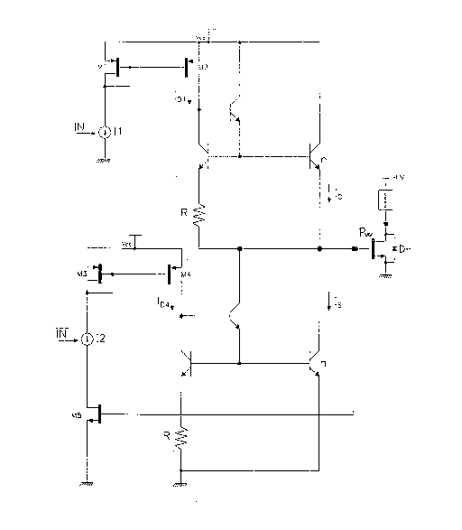
The electrical diagram of Fig. 9 shows an embodiment
of the circuit of the invention in the case of a
driving circuit which, under other aspects, may be
entirely similar to the functional circuit of Fig. 6.
The switch (OFF) of Fig. 8 is constituted by a MOS
-~ transistor M5 in the example shownO
When the power transistor Pw switches-off, while its
gate voltage drops, also the gate voltage of the tran-
~, sistor M5 decreases.
In this switching-off phase, the resistance Rdson of
the transistor M5 increases, thus causing a "mismatch"
between the currents Il and I2. By dimensioning the
transistor M5 so that such a "mismatch" manifests it-
self in a significant manner when the power transistor
Pw has already come out of saturation, the mismatch
will not represent practically any problem because the
power transistor has already switched-off. Of course,
the transistor M5 may be dimensioned in a way that its
:. -,
, ~
2~20~8~
. !
: ~ .
Rdson be practical]y ne~llgeable until the gate l)oten-
~` tial of the output power transistor has dropped to a
value that has surely made the power transistor Pw e.~iL
a saturation condition.
~i? 5 Therefore, the transistor M5 behaves as a switch
`': that opens when the gate voltage of the power transis-
tor drops below the value of the threshold voltage of
: M5, thus interrupting the current flow in the branch I2
of driving circuit.
~;` 10 The introduction of a switch (M5) in series with the
current generator (I2), does not modify other func-
1 tional characteristics of the driving circuit, which
retains its speed characteristics, moreover rise and
..
~ fall times may remain are identical to each other and
,~:15 more generally may be controlled. On the other hand the
static consumption of current when the power transistor
is off is totally eliminated. T}le circuit arrangement
~,of the invention is simple to implement and requires a
m:inimum additional area of intecJration.
,~ 20
~ :~
1 `,-~.~
,.~
}.~
:~! 30
~' ~'"`;J
',".'.~ '
....,,1
~ ,
; ,~,,j
i~
~1, 7
', 'I
,~:
:'~