Note : Les descriptions sont présentées dans la langue officielle dans laquelle elles ont été soumises.
212181'~
DEVICE FABRICATION ENTAILING
PLASMA-DERIVED X-RAY DELINEATION
B~ round of the Invention
Technical Field
The invention relates to fabrication of devices built to submicron design rules.Plasma-derived x-ray radiation serves for pattern delineation for small featuresconsidered un~tt~in~ble by use of longer wavelength electromagnetic radiation. The
plasma source is matched to a projection camera operating in a ringfield sc~nning
mode. Very Large Scale Integration ("VLSI") is a prime objective.
Description of the Prior Art and of Co-pending Canadian Patent
Application Serial No. 2,121,608, filed April 19, 1994.
State-of-the art VLSI is a 16 megabit chip with circuitry built to design rules
of 0.5 ~m. Effort directed to further mini~tllrization takes the initial form of more fully
lltili~ing resolution capability of presently-used ultraviolet ("UV") delineating radiation.
"Deep" UV (~=0.3 ,um - 0.1 ~m), with techniques such as phase m~king, off-axis
illumination, and step-and-repeat may permit design rules (minimum feature or space
dimension) of 0.25 ~m or slightly smaller.
At still smaller design rules, a different form of delineating radiation is
required to avoid wavelength-related resolution limits. An extensive effort depends on
electron or other charged-particle radiation. Use of electromagnetic radiation for this
purpose will require x-ray wavelengths.
Two x-ray radiation sources are under consideration. The first, the electron
storage ring synchrotron, has been used for many years and is at advanced stage of
development. Electrons, accelerated to relativistic velocity, in following their magnetic-
field-constrained orbit, emit x-ray radiation. Radiation, in the wavelength range of
consequence of lithography, is reliably produced. The synchrotron produces precisely
defined radiation to meet the demands of extremely sophisticated experimentation but is
a large, very costly piece of apparatus.
Plasma x-ray sources are less costly. These depend upon a high power, pulsed
laser - e.g. an yttrium aluminum garnet (YAG) laser, or an excimer laser, delivering
500-1,000 watts of power to a 50 ~m-250~m spot, thereby heating a source material to
e.g. 250,000~C, to emit x-ray radiation from the resulting plasma. Plasma sources are
'~ '
2121819
compact, and may be dedicated to a single production line (so that malfunction does not
close down the entire plant).
A variety of x-ray patterning approaches are under study. Probably the most
developed is proximity printing. In this approach 1:1 im~ging is produced much in the
manner of photographic contact printing. A fine-membrane mask is m~int~ined at one
or a few microns spacing from the wafer. This spacing lessens likelihood of maskdamage, but does not elimin~te it. Making perfect masks on a fragile membrane
continues to be a major problem. Necessary absence of optics in between the mask and
the wafer necessitates a high level of parallelicity in the incident radiation. X-ray
radiation of wavelength ~<16A is required for 0.25 ,um patterning to limit scattering at
feature edges.
Use has been made of the synchrotron in proximity printing. Relatively small
power resulting from the 10 mrad-20mrad arc of collection, together with the high-
aspect ratio of the emission fan, has led to use of a sc~nning high-aspect ratioillumination field (rather than to full-field im~ging).
Projection lithography has natural advantages over proximity printing. Camera
optics in between the mask and the wafer compensate for edge scattering and, so,permit use of longer wavelength radiation. Use of "soft x-ray" in the ~=lOOA-200A
wavelength range increases the permitted angle of incidence for glancing-angle optics.
The resulting system is known as soft x-ray projection lithography (SXPL).
A favoured form of SXPL is ringfield sc~nning. The long narrow illumination
field is arc-shaped rather than straight, with the arc being a segment of the circular ring
with its center of revolution at the optic axis of the camera. Use of such an arcuate
field avoids radially-dependent image aberrations in the image. Use of object:image
reduction of e.g. 5:1 results in significant cost reduction of the, now, enlarged-feature
mask.
Co-pending CAn~ n Patent Application Serial No. 2,121,608, filed April 19,
1994 describes and claims device fabrication using synchrotron derived x-ray radiation.
SXPL is one form of lithography described and claimed.
It is expected that effort toward adaptation of plasma x-ray sources for SXPL
will continue. Design of collection and processing optics - design of the condenser - is
complicated by the severe mi~m~tch between the plasma emission pattern and that of
the ringfield scan line. A typical plasma x-ray source has a 1:1 aspect ratio emission
, .
': A
2121819
3 -
pattern. The required scan line is likely greater than 10:1.
Summary of the Invention
Ringfield projection lithographic definition in the fabrication of 0.25 ,um and
smaller design rule devices makes use of an x-ray plasma source. Requirements for
5 illumination uniformity, and for other characteristics of the illumination field, necessary
for matching the projection camera, are met by a novel condenser. The collector lens -
the condenser lens on which the plasma radiation is first incident - includes a number
of pairs of facets which are symmetrically placed with respect to the plasma. Each
facet collects radiation from a sector of the emission and images the entire radiation
10 field, to produce an image intensity which is the sum of the facet intensities. Facets are
complementary so that any gradation in intensity of its field image is equal andopposite to that of its twin. In this way a constant intensity field is effectively
produced from essentially the entirety of the plasma emission without need for
stitching. Facets may be planar or may be shaped to increase collection angle, the only
15 requirement being that size and shape of paired members be truly complementary so as,
together, produce an evenly illumin~te~l composite image.
Species of the invention provide for processing optics for shaping, for
directing, and for adjusting divergence of the illumination field as made incident on the
reflecting mask. The condenser is of a~propliate design for proper pupil fill and for
20 matching other camera requirements. The design is suitable for use with reduction
projection, e.g. for 5:1 subject:image reduction.
In accordance with one aspect of the present invention there is provided
process for fabrication of a device comprising at least one element of at least dimension
< 0.25 ~m, such process comprising construction of a plurality of successive levels,
25 each level ent~iling lithographic delineation, in accordance with which a subject mask
pattern is imaged on an image plane, ultimately to result in removal of or addition of
material in delineated regions, at least one such level ent~iling ringfield projection
lithographic delineation by use of radiation in the soft x-ray spectrum, and in which
such radiation is derived from a laser-produced plasma CHARACTERIZED IN THAT
30 emission from the plasma is collected by a collector lens including at least four paired
mirror facets, in which members of each pair are symmetrically disposed about an axis
of the source and in which paired members individually produce complementary images
2121819
- 3a-
of the entirety of an illumination field, whereby paired members together produce an
evenly illllmin~tçd compensated field and the entire illumination field is of an intensity
which is the sum of all facet-produced image fields.
5 Brief Description of the Drawin~
FIG. 1 shows a plasma x-ray source with pump and focusing means.
FIG. 2 shows a state-of-the art condenser for collecting plasma radiation and
for ill~ in~tin~ a ringfield arc on a mask for delivery to the camera pupil.
FIGs. 3 and 4 are elevational and plan view of condenser optics of the
10 invention, showing im~ging of the radial and circumferential aspects of the ringfield
image.
FIG. 5 is a detailed view of a processing mirror for shaping the illumination
field.
FIGs. 6a, 6b and 6c show a condenser lens arrangement using quadrupole
15 distribution analogous to that ~ elllly used in UV p~ttçrning.
FIGs. 7a, 7b, 7c and 7d are plan views of alternative paired-facet collector lens
arrangements satisfying the inventive requirements. FIG. 7e is an elevational view of
FIG. 7b.
4 2121~19
FIGs. 8a and 8b are orthogonal views of an illustrative 3-lens condenser
with output successively illuminating a mask, properly filling a camera pupil, and
scanning a wafer.
Definitions
S Plasma Source - A thermally-produced plasma for yielding x-ray radiation -
generally pumped by a high power pulsed laser.
Illuminaffon Radiation - The delineating radiation as incident on and producing an
min~tlon Field on the mask, characterized by intensity, direction, divergence
and spectral width.
10 Divergence - As used by itself, the term refers to mask divergence, i.e., the largest
angle about the axis of the cone of radiation as incident on the mask. In projection,
the axis is generally a few degrees off normal incidence as required for reflection
masking. The magnitude of divergence required in projection is that needed to
reduce ringing at feature edges to the éxtent necessary for desired resolution and
15 contrast. In full-field exposure, divergence should be similar at every illumination
point. In scanning, some non-uniformity in the scanning direction may be averaged
out.
Condenser - Optical system for collecting radiation from the plasma source, for
processing the radiation to produce a ringfield illumination field, and for illumin~ting
20 the mask.
Collecting Optics (or Collector) - The Optics within the condenser responsible for
collecting the plasma-derived radiation. The collector has a focus.
Processing Optics - Optics, in addition to the collecting optics, within the condenser
for processing collected radiation for delivery to the mask.
25 lm~ging Optics - Optics following the condenser responsible for delivering mask-
modulated radiation to the wafer, i.e. the camera optics.
Camera Pupil - Real or virtual aperture which defines the position through which
2121~19
illumination radiation must enter the camera, of angular size defining the diffraction
limit of the camera. Its physical size is that of an image of the real limiting aperture
of the camera.
Lens - The term is used in this description to define any optical element which
5 causes x-ray radiation to converge or diverge. "Lenses", in x-ray systems, aregenerally reflecting - are sometimes referred to as "mirrors". Contemplated lenses
may be multi-faceted or may be non-faceted, i.e. continuous - e.g., of ellipsoidal or
other curvature. The convergence or divergence is a result of action analogous to that
of a tr~n~mi~ion optical lens.
10 Facet - Individual segment of a lens - either a separate element, or part of a
monolithic structure, which, generally in concert with other facets, is responsible for
convergence or divergence of the radiation. Individual facets may be planar or
curved.
Scatter Plate - Optical element for increasing divergence. Divergence may be in one
15 or two dimensions.
Detailed Description
General - There is a continuing effort directed to development of x-ray plasma
sources for pattern delineation at feature sizes <0.25~m. See, W. T. Silfvast, M.C.
Richardson, H. Binder, A. Hanzo, V. Yanovsky, F. Jin, and J. Thorpe, " Laser-
20 Produced Plasmas for Soft-X-ray Projection Lithography" J. Vac. Sci. Tech. B 106,
Nov./Dec. 1992, pp. 3126-3133. By its nature, emission from a plasma source is
omnidirectional. Device fabrication of this invention depends upon a condenser
designed to capture this omnidirectional emission and to shape it to produce a high-
aspect ratio illumination field for ringfield projection lithography.
In addition to shaping, directing, and tailoring divergence, the condenser
must filter the natural plasma spectrum of perhaps ~=50A - 400A to yield the
favored ringfield wavelength range within a spectrum of ~= 100A - 200A (at this
time the preferred spectral range is ~= 125A - 140A). Use of this "soft x-ray
projection lithography" (SXPL) takes advantage of ability to make high reflectivity
30 normal incidence mirrors. It also expedites use of glancing mirror optics, inpermitting larger angles of incidence than those required for the "hard x-ray" used in
proximity printing.
2121~9
- 6 -
Filtration, to yield the desired x-ray spectrum, will likely use multi-layer
reflectors (MLR) operating on the Distributed Bragg Reflector (DBR) principle.
The Drawing - Detailed design and processing information is discussed in
conjunction with the figures.
S In FIG. la YAG or excimer laser 11 emits a beam 12 which is focused
by lens 13 to heat a spot 14 on target material 15, thereby yielding plasma ball 16
which emits x-ray rays 17. Radiation is emitted over an entire 180~ half sphere.FIG. 2 is a perspective view of a state-of-the art system for using a
plasma source for powering a projection camera. Plasma source 21 emits a half
10 sphere of x-ray radiation shown as rays 22. An MLR 23 focuses radiation at focus
24 on mask 25. The illumination field is an image of the source. As depicted, the
illumination field is a spot 24 incident on mask 25, where the radiation is either
trAn~mitted or reflected to be introduced into camera 26 by partially filling entrance
pupil 27. For the proper pupil fill shown only a relatively small cone of radiation is
15 collected, and radiation outside this cone is wasted. If the size of the condenser is
increased in order to collect the relatively large angle radiation represented rays 28,
~he camera pupil is greatly overfilled as shown by field 29, produced by the
condenser-emitted rays shown as broken lines. Energy is wasted and the image is
degraded. Neither arrangement produces a ringfield illumination field.
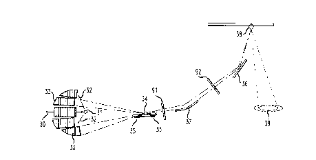
FIGs. 3 and 4 show an illustrative system for effectively producing the
high-aspect ratio illumination field for ringfield projection. FIG. 3, an "elevational"
view illustrates processing to deliver the short dimension of the high-aspect-ratio
field. Plasma 31, produced by laser beam 30 emits x-rays 32 over a wide angle,
near-half sphere, which is captured by lens facets 33. While not seen in this view,
25 most or all of facets 33 are members of paired complementary facets, common to all
collectors used in the inventive processing. An aperture can be placed in the beam
path, either at position 91 or 92 in FIG. 3, (~93 or 94 in FIG. 4). The aperture can
block part of the beam to produce greater uniformity in intensity on the mask, if
needed. If ellipsoidal, the first focus may conveniently correspond with the source,
30 and the second focus may correspond with the image. The curved facet surface may
be of "Lopez" form. The Lopez mirror is explicitly designed to produce a single
focus for many-angled emission. Its use for the individual facets of the multi-faceted
collector lens may be justified.
-7- 2~2l~
Each of the facets may be viewed as having an effective height
comparable to that of mirror 23 in FIG. 2 to produce a field dimension in the
scanning direction which is the same as that of a spot 24. Each of the facets focuses
an image of source 31 as image 34 on lens 35. Lens 35 is a many-faceted mirror
S which directs reflected radiation and overlaps individual beams at processing optic
36. Mirror 37, likely a single, continuous surface, concave lens, is a redirecting optic.
The several images are brought to a common focus at or near mask 38 and are
directed to enter camera pupil 39.
Companion FIG. 4 shows illumination of the transverse (or long
l 0 dimension) of the high-aspect-ratio ringfield. Laser plasma radiation from source 40
is collected by the array of ellipsoidal mirrors, here shown as paired facets 41a-41b.
The collector focuses an image of the source to a series of spots on processing lens
(mirror array) 42, with individual spots made incident on individual facets of lens
42. The facets of lens 42 are oriented such that the center ray of the reflected beam
15 strikes the center of the processing lens 43 which is again a multi-faceted array in
this example, but may be a continuous curved surface such as a cylindrical mirror or
an ellipsoidal or toroidal mirror. The distance between the processing lens 42 and
processing lens 43 is such that the processed radiation emitted by lens 42 covers the
length of lens 43. Lens 43 in conjunction with lens 37 of FIG. 3, together, shape the
20 beam to produce the proper arc shape illumination field 44 as incident on mask 45.
The same optics introduce the convergence shown upon reflection from mask 45 to
produce the desired fill of entrance pupil 46.
The multi-faceted lens 50 shown in FIG. 5 is illustrative of optics
serving the function of lens 42 of FIG. 4. Lens 50 is constituted of 8 facets 5125 oriented such that incoming cones of radiation 52 are reflected as cones 54 toward
the processing optics. The aspect-ratio of facets 51 may approximate that of thedesired illumination field - image dimension 53 corresponding with the long
dimension of facet 51.
In FIG. 6a, collector facets 60 are arranged to have a quadrupole
30 distribution, to focus into two series of spots on multi-faceted lens 61 (e.g.
corresponding with lens 42 of FIG. 4). In FIG. 6b, it is seen that facets 61 are split
along their length so that each consists of two facets 62, oriented at different angles
to result in radiation being reflected in two slightly different directions 63 in the
vertical or scanning direction. Viewed from FIG. 6c, radiation upon reaching the35 pupil is split into four separate multi-image fields 64, 65, 66 and 67.
~ 2 ~ 21~1Y
- 8 -
FIGs.7a-7d show various collector lens designs, always including
paired complementary facets. Discrete compensating facets separate lens functions
and facilitate design. Members of pairs, always producing equal and opposite
intensity gradients, to, together, produce a composite image which is evenly
5 illllmin~ted in the compensating direction, are independently directed to suit the
camera optics. Illumination in the compensating direction is at least + 15%. Careful
facet placement results in + 5% or even + 1% or better.
In FIG.7a, the lens array 70 is constituted primarily of paired facets
71a-71b. Facets 71c, positioned at the extremities of the emission sphere, are not
10 paired. Pairing, here to, is preferred in principle, but any intensity gradients may be
small enough to be ignored. In general, single-faceted mirrors over the final 65 - 75 ~
of emission in this direction are tolerable. (Consistent with usual practice, angles are
measured relative to the optic axis.) As in all arrangements, members of paired
facets are symmetrically placed about source 75.
In FIG.7b, collector lens 72 is constituted of five pairs of facets 72a-
72b. This arrangement may result in a somewhat smaller aspect-ratio slit than the
7-tier arrangement of FIG.7a. The variations of FIGs.7c and 7d are trivial. For the
four-tier arrangement of facets 73a-73b, the horizontal center line of spot source 75
is naturally located at the intercept of two pairs. It is of little importance that
20 source-to-facet spacing is different in the two dimensions - it is desirable only that
each dimension spacing be symmetrical. Collector lens 74 is a three-tier array of
paired facets 74a-74b. Illustrative facet aspect-ratio may be suited to a similarly
shaped illumination field.
FIG.7e is an elevational (or side) view of the arrangement of FIG.7b,
25 showing stacked facets 72a.
The facet arrangements shown are based on minim~l facet count. The
inventive requirements may be met by higher count arrangements. As an example,
lateral faceting may involve four rather than two facets, providing that inner and
outer pairs produce the required evenly-illumin~ed composite field image. Should30 there be reason to do it, it is required only that the entire lateral set produce such a
field image (so that neither the inner nor the outer pair is completely self-
compensating).
FIGs. 8a and 8b are plan and vertical views, respectively, showing a
three-lens condenser system used as the basis for Example 1. Collector lens 80
35 includes five paired facets of the arrangement shown in FIG.7b. The facets are
MLRs, consisting e.g. of 40 paired Mo-Si layers. The radiation passes through a
2 1 2 i 8 1 9
window 88 that keeps dirt produced by the plasma from ~l~m~ging the mirrors of the
camera 86. The first processing lens 81, a grazing incidence multi-faceted mirror,
directs the radiation to processing lens 82 which combines the functions of vertical
processing lens 37 of FIG. 3, and horizontal processing lens 43 of FIG. 4. Processed
radiation as leaving lens 82 produces arc-shaped illumination field 83 on mask 84,
which in turn, creates an image of the arc on wafer 87 via reflection into camera pupil
85 of camera 86.
Device Fabrication - Basic device fabrication is not otherwise altered.
Reference may be made to a number of texts, e.g. Simon Sze, VLSI Technology,
McGraw Hill, 1983. The following examples 1 and 2 are directed to the critical
window level in MOS VLSI device fabrication.
Example 1 - Fabrication of a 256 mbit, 0.1 ~m design rule MOS device is
illustrated by fabrication at the window level as follows: The apparatus of FIGs. 8a
and 8b is provided with a plasma source of 500 watt emission consisting of a 500 watt
YAG laser-pumped tin source. The collector lens of the arrangement of lens 80
consists of eight 35mm x 90mm multi-layered facets, each cont~ining 40 pairs of
successive Mo-Si layers, to result in focused beams of ~=135+3A of total power 2.5
watts. As received by wafer 87, the ringfield sc~nning line is of dimensions, 1 mm in
the sc~nning direction and 25 mm as measured along the chord of the arcuate line.
Example 2 - The x-rays projection camera is of the family designed by Jewell.
It has a numerical aperture of 0.1 and is capable of printing 0.1 micron lines. In the
first applications it will be used only for the critical levels, e.g. the gate and the contact
windows. Other printers, e.g, deep UV, will print other levels. In later models, when
the numerical aperture has been increased to 0.2, it will print critical levels with 0.05
micron features and also many other levels - the other levels will have 0.1-0.15 micron
features that are too small to be printed even by Deep UV. Suppose 1 watt strikes the
mask of the gate level. Due to losses in the mirrors of the camera, a thin silicon
window (0.3 llm thick) between the wafer and the camera, only 75 ~lm (or less,
depending on how much of the mask is reflective) arrive on the wafer.
The wafer has p~ rning from previous levels. Immediately before the
lithography, the wafer was coated with a very thin oxide layer, a polysilicon conductor
and on top, a thick oxide layer. An x-ray resist covers the whole wafer.
- 10-
The wafer is placed under the x-ray projector, aligned, and exposed. If the resist has
a sensitivity of 15mj/cm2, Scm2 will be exposed each second.
The resist is developed, and, where there is no resist, the top oxide and
polysilicon layers are removed by dry etching, leaving the very thin oxide layer on
S the bottom intact. Later an ion beam implants dopants through the thin oxide into
the silicon, forming conductive layers that act as source and drain regions. Theregion of silicon under the polysilicon gate remains resistive, and will conduct only
when a voltage is applied to the gate.