Note : Les descriptions sont présentées dans la langue officielle dans laquelle elles ont été soumises.
wo 93/155~ ~1 h i3 ~ 7 ~ pcrlus93/oo7s1
TENIPERATURE COMPENSATION OF A
CRYSTAL REFERENCE USING
DIRECT DIGITAL SYNTHESIS
Technical Field
This invention relates generally to temperature
compensation circuits, and more specifically to a crystal reference
tempsrature compensation circuit.
.
Background
1~ Crystal oscillator circuits vary in output frequency due to
variations in the resonant frequency of the circuit's crystal
reference elernent. These variations to the crystal element are
typically caused by changes in temperature which affect the
crystal elements resonant frequency. A few techniques which are
used in the art for compensating for these crystal variations
include: using crystals having good temperature characteristics;
using crystal ovens to main~ain the crystal's temperature at a
substantially constant temperature; and characterizing the crystal
over temperature and compensating for these characteri~ed
2~ variations by providing a compensation signal to the osciliator
circuit which attempts to offset the variations in the crystal, such as
discussed in lJ.S. Patent 4, 967, 165 by Lee et al.
The major problem with using high quality (e.g, minimal
temperature variation crystals~ crystals as described above is that
high quality crystals tend to be very expensive and still tend to
vary a substantial amount over temperature. The use of crystal
ovens are not only expensive since they require quite a bit of
parts to implement, but they also tend to be impractical for battery
powered applications due to their high current drain. Known
compensation techniques that compensate forcharacterized
crystal variations do not provide the frequency stability required
for modern communication equipment having high specifications.
2125~7 ';'
wO 93/15555 PCI'/US93/~OjSL s
Present day frequency synthesizers normally utilize
varactors to vary the resonant frequency of the crystal oscillator in
order to change the phase-locked-loop (PLL) output frequency.
Voltage curves corresponding to different temperatures are also
5 typically programmed over the operating temperature range of
the synthesizer into the PLL. The programming, in turn, sets
current sources which are enabled at certain temperatures and
drive the oscillator varactor differently over temperature in order to
compensate the circuit for changes in temperature. The problem
10 with the above compensation scheme is that the synthesizer
requires the use of a varactor to adjust the oscillator's frequency.
The varactor not only adds additional cost to the circuit but also
adds it's own tolerances to the final generated frequency.
A need thus exists in the art for a way of eliminating the
15 use of tight temperature characteristic crystal elements and still be
able to provide for a crystal oscillator circuit which exhibits
extremely' small outpùt frequency variations over temperature. A
need also exists for a way of elirninating the need for using
varactors in the synthesizers oscillator circuit as the circuit's
20 tuning vehicle.
Summary of the Invention
Briefly, according to the invention, a temperature
compensated oscillator circuit comprises a reference oscillator
25 circuit for generating a reference oscillator signal. A digital
synthesizer means for receiving the reference osciilator signal
and providing an oulput signal having a predetermined
frequency. The temperature compensated circuit further
includin~ a compensation means for providing a compensation
30 signal to the digital synthesizer means in order to maintain the
output signal substantially at the predetermined frequency over a
given temperature range. In another aspect of the invention, a
radio comprises a receiver and a temperature compensated
oscillator circuit.
:
WO 93/15555 ~12 ~ 8 7 ~ PCI/US93/00751
Brief Description of the Drawings
FIG. 1 is a block diagram of a reference oscill,~tor crystal
temperature compensation circuit utilizing direct digital synthesis
with PLL synthesizer circuit in accordance with the present
5 invention.
FIG. 2 is a block diagram of a radio in accordance with the
present invention.
Detailed Description of the Preferred Embodiment
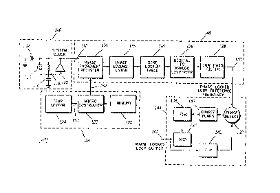
Referring now to the drawings and specifically to FIG. 1,
there is shown a system block diagram o~ a PLL synthesizer 100
in accordance with the present invention. The invention utilizes a
digital synthesizer means such as direct digital synthesizer (DDS)
148 and a conventional phase-lock-loop (PLL) synthesizer
15 section 144 as known in the art. The DDS section 148 comprises
a phase increment register 114, a phase accumulator 116, a sine
look-up table 118, a digital to analog converter 126, and an anti-
aliasing filter such as low-pass filter 128. The digital synthesizer
148 accumulates phase changes at a higher clock frequency and
20 generates a lower frequency output signal. Sampling theory
requires that the generated signal be no more than one-half of the
reference clock input signal.
A typical oscillator circuit such as system clock circuit 146
comprises a crystai element 104, resistor 108, capacitors 102 and
25 106 and inverter 110 to provide a square wave system clock
signal 112 ~or the digital synthesizer. The problem with crystal
references, such as crystal eiement 104, is that their resonant
- frequencies vary over temperature. The present invention
compensates for these variations by utilizing a compensation
30 means such as compensation section 154, which comprises a
control means, such as microcontroller 122. Microcontroller 122
can be a microprocessor or microcontroller as known in the art.
Also part of compensation section 154 and coupled to the control
means 122, is a storage means 120. Storage means 120 can be
35 an external memory device such as external ROM, etc., or can be
internal to the microcontroller 122 . Appropriate control software
is also stored in storage means 120.
.~
WO 93~ 7 ~ Pcr/usg3/007s; ?
As part of the present invention, crystal 104 is tested and
graded and the crystal information is stored in storage means
120. Pre~erably, the crystal operating characteristics are
determined at least on a per degree Celsius scale or better. For
5 example, the resonant frequency of crystal 104 is determined on
a per degree Celsius change over a predetermined operating
temperature range (e.g, -20 to +60 degree Celsius). Thereby,
compensation for shifts in frequency of crystal 104 due to
variations in temperature.
This shift in frequency of crystal 104 over temperature is
translated to phase increment inforrnation that is stored in
memory 120. This phase increment information (values) is the ;
required phase increment value for generating a predetermined
output signal 130 given a predetermined system clock signal -
15 (reference oscillator signal) 112. In operation, the system clock
frequency 112 must be at least twice the generated frequency in
order to meet the Nyquist rate criteria.
Given that the output signal 130 is a predetermined
frequency (e.g., 864 KHz) and the system clock frequency is also
20 known (e.g, 16.8 MHz), compensation for shifts in the system
clock signal (reference oscillator signal) 112 can be done by
providing a different phase increment value (compensation
signal) to the digital synthesizer 148 in order to maintain the
output signal frequency 130 substantially constant over changes
2~ in ambient temperature which affect the crystal 104. Since the
crystal 104 has been characterized over temperature, the
appr~priate phase increment values are inputted to the phase
increment means 114 in order ~or the digital syn~hesizer 148 to
generate an output signal 130 having a subslantially constant
30 frequency over a given temperature range which atfects the
~requency of the system clock signal.
The value stored in the phase increment register 114 is
added to the phase accumulator once during each clock cycle
(system clock signal 112, preferably at the positive clock edge).
35 The value sent to the phase increment register by control means
122 (on a per clock cycle basis) is dependent on the ambient
temperature experienced by crystal 104, as determined by
21 ~ ~ ~J 7 h
WO 93/15~5~ PCI /US~3/00751
temperature sensing means 124 which is coupled to control
means 122 and is part of compensation section 154.
Temperature sensing circuit 124 can be a conventional diode
contiguration which generates a temperature signal 150 in
5 accordance with the ambient ~emperature.
The phase increment value to be stcred in phase
increment register 114 is determined by control means 122 once
the crystal operating temperature is measured by temperature
- sensor 124, at which point the corresponding phase increment
10 value is recovered from memory 120 and sent to phase increment
register 114. For example, if the temperature sensed by
temperature sensing means 124 is determined to be 27 degrees
Celsius, the phase increment value ~or this temperature is
recovered from memory 120 and sent to phase increment register
15 114 as compensation signal 152. The manner of calculating the
phase increment value will be discussed later in the description.
At every system clock cyc:e, the value stored in the phase
increment register 114 is sent to a phase accumulator means
such as phase accumulator 116 where the phase incrernents are
20 summed. The output of the phase accumulator 116 which is the
instantaneous phase value is in turn converted into a sine
amplitude by the sine look-up table 118. The amplitude bit
~- stream is then converted into an analog signal by the digital to
analog converter (DAC) 126. The converted signai not only
contains the desired sine wave as its major component, but also
includes the higher frequency image components due to the
conversion of a sampled wave-form. In order to reduce the image
signals to a desirable level, a iow pass filter 128 is added. The
Iqw pass corner frequency ~of filter 128 must be equal to or less
than half the sampled frequency. Once a complete sine wave is
generated (DDS generated signal 130) the phase accumulator is
cleared (reset) and the process begins again in order to generate
the next sine wave which forms the temperature compensated
output signal 130.
The DDS generated signal 130 which has been
temperature compensated can then be utilized as the reference
oscillator signal in a conventional PLL synthesizer 144. The PLL
~12~ . t ~
WO 93/15~5~ PCr/US93/00751'
circuit 144 comprises: a phase detector 132, charge pumps 134,
divider circuit 140, loop filter (Fs) 136 and VCO 138, as known in
the art and which provide the PLL output signal 142. The PLL
output signal 142 can then be coupled to transmitter and receiver
5 circuits (not shown) in order to torm a radio. The reference signal
130 into the phase detector 132 may be squared off using a
comparator in order to avoid jitter if required, depending on the
application.
A typical example using the present invention yields the
1 0 following:
FG Fs (~0~ where, ~G= Generated Frequency
- Fs = Clock Frequency
a0= Phase Increment Value
N = number oS bits in phase
1 5 accumulator
Assuming a 16.8 MHz reference crystal 104 as the system clock
for the DDS/ PLL synthesizer circuit 100, and phase accumulator
116 and phase increment register 114 being 32-bit devices and
20 also wanting to generate a 864 Khz signal 130. We can
calculate the required phase increment value as follows:
2N FG ~732(864 X 1 03)
FS ~ 16.8 X lo6
~0 = 220884032.4 to generate 864 KHz.
Given that FG is known, a corresponding phase increment
value on a per degree Celsius (or higher resolution basis, e.g.,
30 every .1 degree CP jSjUS) jS stored in memory 120, in order to
have a substantially constant FG . Since Fs (system clock
frequency 112~ varies wi~h temperature due to the crystal's
frequency variation over temperature, the above calculation is
performed for all measured temperature reference points in the
35 relevant temperature range, thereby memory 120 has stored a
look-up table with different phase increment values
corresponding to different temperatures for oscillator circuit 146.
7~J
WO 93/15~55 PCI'/US93/00751
7 ~-
The ambient temperature is measured as close as possible to
crystal 104 and a compensation signal 152 is ssnt to phase
increment register 114 every every clock cycle of system clock
signal 112.
In practice the .4 of the above value a0 of is eliminated
from the above result giving an FG ~f:
~0 Fs ~ 40~? ( 1 ~ RX 1 ~6)
FG ~ 2N = 23 2
FG = 863,999.9988 Hz.
The frequency resolution is then calculated as follows:
Frequency resolution = 2S
R s I tio 16.8X~06 0003g11555H
This can, in turn, be calculated in terms of parts-per-million (PPIJI)
25 at 864 KHz as follows:
0 864 = 0.004527263 PPM change for every bit
increment in phase. The larger the number of bits in the phase
30 increment register 114, the better the resolution o~ the output
signal. The limiting factor for the temperature com,~ensating
circuit will probably lie in the temperature sensing sensor 124 and
how accurately quickly it can detect changes in temperature~ As
the clock frequency increases, the temperature sensor must be
35 able to sense temperature changes faster unless the phase
increment (compensation signal 152) updates are not sent on a
per clock cycle basis (e.g, every two clock cycles, etc.).
By incrementing a0 by one, the delta change in FG that
takes place can be seen.
21Z6~ )
W0 93/15~5~ Pcr/Us93/oojs~ '
220884033(16.8 MHz)
F~; = 232
FG= 864,000.0027 Hz
s
= 0.0039 Hz delta change.
As been shown by the above calculations, by utilizing the
present invention very low crystal resolutions can be obtained
(0.0039 Hz in the above example). The reference frequency
range is from 0.0039 Hz to 50% of the clock frequency ~in this
example .0039 Hz to 8.4 MHz), therefore it is possible to use a
wider range of crystal elements as crystal element 104 as long as
the element has been characte~ized as the resonant element 104
as previously described. The present invention also allows for a
low-cost crystal having bad over-temperature characteristics to be
used given that once the crystal has been characterized over
temperature, the digital synthesizer 148 provides for extreme~y
high frequency resolution for output signal 130, as been shown.
Preferably, crystal 104 should be a high frequency crystal
in order tor different output signals 130 to be allowed to be
generated. The present invention allows for different output
signals frequencies to be generated once the crystals frequency
behavior over temperature has been converted into appropriate
2~ phase increment values over temperature. Memory 120 can store
different sets ot phase increment values for different output signal
frequencies which may be desired. Another technique could
allow for micro~onlroller 122 to calculate the required phase
increments in order to produce a given output signal using a
characterization table of changes in clock signal frequency 112
due to changes in temperature affecting crystal 104. Thereby,
only the changes in frequency of crystal 104 over temperature
would have to be stored in memory 120. Phase increment
values for different output signals having different frequencies in
this case would not have to be pre-stored in memory 120,
allowing ~or more system flexibility and less costlier memory
,, .
~126~72 ~
WO 93/15~ ; P~/US93/00751
r 9
devices. As shown in the synthesizer circuit schematic of FIG. 1,
no varactor is required as the osciltator circuit's tuning vehicle.
In FIG. 2, there is shown a block diagram of a radio 200 in
accordance with the present invention. Block 100 is the DDS/PLL :
5 (phase-lock-loop) synthesizer with temperature compensation
crystal circuitry described in FIG. 1. The PLL output signal 142 of
circuit 100 is coupled to a conventional transmitter 202 and
receiver 206 as known in the art. Radio 200 is controlled by a
controller 204 such as a microprocessor or microcontroller as
10 known in the art. Controller 204 provides control for both
transmitter 202 and receiver 206. An antenna switch 208 under
the control of contro!ler 204 selectively couples the transmitter
202 and receiver 206 to antenna 210. Antenna switch 208 can
be a duplexer or circulator, depending on the radio application at
1~ hand. Radio 200 can be a radio frequency ~RF) two-way radio
such as a time division multiplexed (TDM) radio.
As can be seen from the abov~ discussion, the present
invention provides for very tight frequency tolerances using very
low cost crystals which can exhibit poor temperature
20 characteristics. The invention also allows for the elimination of
the varactor as the tuning element for the oscillator circuit of the
PLL synthesizer. By using one high frequency crystal reference
104, a very wide range reference signal 130 can be generated by
the DDS temperature compensation circuit disciosed in the
25 present invention.
What is claimed is: