Note : Les descriptions sont présentées dans la langue officielle dans laquelle elles ont été soumises.
WO 94/23491 ~13 6 ~ 4 3 PCT/US94/03299
-
-- 1 --
POWER AMPLIFIER BIAS CONTROL CIRCUIT AND METHOD
S BACKGROUND OF THE INVENTION
~ield of the Invention
This invention relates to controlling the gain of RF
power amplifier~. Specifically, an FET power amplifier is
caused to have substantially constant operating
10 characteristics by maintaining the amplifier current
constant for a given output power in spite of fluctuations
in ambient temperature, load, and supply voltage.
Description of the Prior Art
FIG. 1 illustrates a prior art transmission circuit
15 of a radio transmitter (e.g., a battery powered trans-
mitter such as an automobile telephone). Amplifier stages
1, 2, 3 are each conventional FET (field effect
transistor) amplifiers including first stage pre-amplifier
1, second s~age driver amplifier 2 and final stage
20 amplifier 3. A common power supply voltage VDD is provided
from a terminal 4 to the drain terminals of amplifier
stages 1, 2, and 3. A fixed gate bias voltage Va is
provided from terminal 5 to the gate terminals of
amplifier stages 1, 2. An example of such an amplifier is
25 the Fu~itsu FMC080802-21 power amplifier.
An RF (radio frequency) signal Sig In is provided at
input terminal 6 to the first amplifier stage 1. Sig In
is amplified to a predetermined level sequentially by
amplifier stages 1, 2, 3; the output of stage 3 is
30 transmitted by antenna 7 to a receiver (not shown). A
bias control voltage provided at terminal 8 to the gate
terminal of final stage amplifier 3 has a magnitude
controlled by additional circuitry (not shown) typically
to be constant, or is varied to be a function of the level
Wo94/~491 PCT/US94103299
~ ~ 3 ., 7 4 ~ -
-- 2
of Sig In. Specifically, when the level of Sig In is
small, the bias control voltage is varied to shift the
operating point of amplifier stage 3 to reduce the drain
current of stage 3. This bias control decreases power
5 consumption of the amplifier and is well known in the
field of battery powered portable telephones.
Generally, the gain of the amplifier of FIG. l is a
function of ambient temperature. When the temperature
rises, the drain current of the FET in each stagè i5
lO reduced, causing a subsequent decrease in gain. This is
shown in FIG. 2 which is an operating characteristic
diagram showing the relation of gain and drain current
versus bias control voltage in the power amplifier of
FIG. l at two temperatures. Curve G~ of FIG. 2 shows gain
15 in dB (vertical axis) versus bias control voltage
(horizontal axis) at room temperature. Curve IDI indicates
variation in the drain current in mA at room temperature
as a function OL control voltage. Points A and C indicate
gain and current at maximum transmission power (bias
20 control voltage a), and points B and D represent gain and
current at minimum transmission power (bias control
voltage b). At point B, where transmission power is at a
minimum, the drain current drawn (and hence power
consumed) by the amplifier are also at a minimum. As
25 transmission power is increased, the drain current must
al~o be increased to prevent saturation and therefore loss
of linearity and gain of the amplifier.
Curves G2 and I~ are the operating characteristic
diagram of the amplifier of FIG. l at an increased ambient
30 temperature, co,~e_~onding to respectively curves G~ and
IDI at room temperature. Point B' on curve G2 represents
the gain of the amplifier at minimum transmission power,
and point D' on curve Im represents the drain current at
minimum transmission power. Point A' on curve G2
35 represents the gain of maximum transmission power, and
point C' on curve I~ represents current at maximum
WO941~491 213 6 7 4 ~ PCT~S94/03299
_ - 3 -
transmission power.
The reduction in both gain and current is readily
seen by comparing points A, B, C, D at room temperature to
points A', B', C', D' respectively at the increased
5 temperatures.
FIGS. 3a-3d illustrate the mechanisms which cause the
fluctuations seen in FIG. 2. FIGS. 3a and 3b are
characteristic diagrams of the drain voltage (horizontal
axis) versus the drain current (vertical axis) as a
10 function of gate voltage of the FET in amplifier stage 3.
In amplifier stage 3, a load curve operating point is
determined by the gate voltage and drain voltage so as not
to cause saturation at maximum transmission power.
Different drain and gate voltages cause different drain
l5 currents, and hence different operating points.
FIG. 3a represents the maximum transmission operating
point at room temperature. The gate bias voltage Va
chosen must correspond to a relatively large drain current
so that the desired maximum transmission power can be
20 achieved. FIG. 3b represents the minimum transmission
operating point at room temperature where the large
current drawn is no longer necescAry to achieve the
desired output power. In order to reduce the D.C. power
drawn by the amplifier, the gate bias voltage (Va) has
25 been decreased. The maximum peak RF output voltage is
e~ ented by the intersection of the load curve of the
drain voltage axis. The reduction in maximum transmission
~OWeL between the two operating points can be seen by
noting that in FIG. 3a the intersection point is V~, while
30 in FIG. 3b the intersection point is VDI which is lower
than VD~. This reduction also corresponds to the loss of
gain as the gate bias voltage is lowered.
FIG. 3c represents the maximum transmission operating
point at an increased temperature. Notice, compared to
35 FIG. 3a, that given the same gate bias voltage (Va) the
drain current has decreased and the maximum peak RF output
W094/~491 PCT/US94103299
~3g74~
-- 4
voltage (as indicated by the intersection of the load
curve to the drain voltage axis) has also decreased. The
reason for the changes is that due to the increase in
temperature, the load curve of FIG. 3c has moved parallel
5 to the original load curve toward the intersection of the
drain voltage and drain current axis. This change with
respect to temperature is a general characteristic of all
FET's.
FIG. 3d represents the minimum transmission operating
lO point at an increased temperature. Similarly the maximum
transmission point and reduction in current and maximum
peak RF transmission voltage can be seen by comparing FIG.
3d to FIG. 3b.
The above diagrams and description deal with an
15 increase in ambient temperature; the inverse situation
occurs for an ambient temperature decrease.
As described above, fluctuations in ambient
temperature cause variations in the drain current, which
in turn cause variations in gain in prior art amplifiers.
20 There is a strong correlation between variations in gain
and variations in amplifier FET drain current as well as
saturation point. Such variations in gain are undesirable
in a cellular telephone system. In a digital cellular
telephone system such as a CDMA system, it is required
25 that a signal received at the base station be controlled
with great accuracy to achieve maximum capacity of the
system. It is therefore undesirable that transmitter gain
vary with temperature.
Gain also varies due to fluctuations both in the
30 power supply voltage and in the load. In such cases,
there is also a strong correlation between variation in
gain and variation in the drain current, so these
variations can be compensated for in the same manner as
the temperature variation.
WO 94/23491 21~ 6 7 4 9 PCT/US94/03299
-- 5 --
SU~ARY OF THE INVENTION
The final amplifier stage of a multi-stage FEr
amplifier is provided with a bias control voltage which
corresponds to the level of the first stage input RF
s signal or alternatively to the desired RF transmission
output power.
In accordance with the present invention, an
apparatus and method control the operating point of a
field effect trancistor (FET) amplifier. Particularly
10 when the FET amplifier is operating over a large dynamic
range where the maximum power generated is significant and
yet current consumption is critical, the present invention
affords an advantage over the prior art. In accordance
with the present invention, there is direct control of the
15 drain current of an FET stage (typically the lact stage)
in order to retain high efficiency without ~aturation over
fluctuations in temperature, output load match, and drain
voltage. The increased stability is achieved through
current control, because current consumption ic the ~ingle
20 most stable parameter in determining the operating point
of a FET stage over varying conditions.
In accordance with the present invention, circuitry
for controlling the current drawn by an FET amplifier
includes a current detector and an integrator. The
25 current detector generates a signal proportional to FET
amplifier drain current, and typically is coupled in
series with a D.C. power source to the drain terminal of
the FET amplifier. The integrator receives two inputs:
the current detector signal and a reference signal which
30 ~oLLe~o..ds to a predetermined amplifier current
consumption for the present operating conditions. The
integrator ou~u-s a control signal which is coupled to
the gate (control) terminal of the FET amplifier. The
control signal at the gate terminal in turn directly
35 controls the FET amplifier operating point, and hence, the
drain current, of the FET amplifier given a fixed
~ ~ ~ 3 ~ 7 4 g
temperature, output load match, and drain voltage. In this
manner, the current of the FET amplifier is controlled in a
closed loop by indirectly controlling the signal applied to
the gate terminal of the FET amplifier.
The reference signal can vary continuously as a
function of input or output RF power, or may be a series of
step functions based on a set of input or output RF power
thresholds. The reference signal corresponds to a current
sufficient to keep the FET amplifier from saturating at high
output RF power, while limiting the current for increased
efficiency at low output RF power.
The invention may be summarized, according to a
first broad aspect, as a power amplifier comprising: an FET
amplifier stage having a power supply terminal and having an
input terminal for receiving an externally provided variable
amplitude signal and receiving a control signal at a control
terminal; a current detector connected to said power supply
terminal thereby detecting a power supply current provided to
said power supply terminal of said FET amplifier stage, said
current detector supplying a signal at an output terminal
proportional to said power supply current; and a comparator
having a first input terminal connected to a source of a
reference signal and a second input terminal connected to the
output terminal of said current detector, and providing in
response said control signal to said amplifier stage.
The invention may be summarized, according to a
second broad aspect, as a power amplifier comprising: an FET
amplifier stage for amplifying an externally provided variable
- 6 -
74769-22
67~9
amplitude signal and having a control terminal; a detector for
detecting a power supply current to said FET amplifier stage
and providing a signal in response thereto; and a circuit for
supplying a control signal to said control terminal of said
FET amplifier stage; said control signal being at least partly
determined by said signal provided by said detector; wherein
said detector comprises a resistance connected between a power
supply source and a power supply terminal of said FET
amplifier stage.
The invention may be summarized, according to a
third broad aspect, as a power amplifier comprising: an FET
amplifier stage for amplifying an externally provided variable
amplitude signal and having a control terminal; a detector for
detecting a power supply current to said FET amplifier stage
and providing a signal in response thereto; and a circuit for
supplying a control signal to said control terminal of said
FET amplifier stage, said control signal being at least partly
determined by said signal provided by said detector; wherein
said control signal is determined by a signal related to an
amplitude of said externally provided variable amplitude
signal and by said signal provided by said detector.
The invention may be summarized, according to a
fourth broad aspect, as a steady operating point amplifier
comprising: an FET amplifier, having a drain terminal for
receiving a supply current and for providing an output signal,
and having a gate terminal coupled to receive an input signal
and coupled to a control voltage; means for providing an
indication of a level of said supply current; a terminal
. - 6a -
74769-22
~ ~ 3~7~
receiving a bias control signal indicating a desired operating
point of said FET amplifier; and means for comparing said bias
control signal to said level indication and producing said
control voltage, said control voltage thereby controlling the
level of said supply current; wherein a desired operating
point of said FET amplifier is maintained constant over
variations in operating conditions.
The invention may be summarized, according to a
fifth broad aspect, as a method for operating an amplifier for
amplifying an externally provided variable amplitudé input
signal to provide a stable operating point over varying
operating conditions and said amplifier having at least one
FET amplifier stage, the operating point of said FET amplifier
stage being determined by a signal applied to a control
terminal of said FET amplifier stage, the method comprising
the steps of: providing said FET amplifier stage as having a
particular level of gain corresponding to a particular level
of a power supply current to said FET amplifier stage, said
particular level of gain being independent of said varying
operating conditions; detecting a level of said power supply
current to said FET amplifier stage; providing a voltage which
is proportional to said power supply current level; providing
a reference signal; comparing said reference signal to said
proportional voltage and generating a signal in response; and
applying the generated signal to said control terminal,
wherein the generated signal causes said FET amplifier stage
to operate at the stable operating point over said varying
operating conditions.
- 6b -
74769-22
7 4 ~
The invention may be summarized, according to a
sixth broad aspect, as a method of operating an amplifier for
amplifying an externally provided variable amplitude input
signal, the amplifier having at least one FET amplifier stage
which amplifies said externally provided variable amplitude
input signal and having an operating point set by a control
signal provided thereto, and having a particular level of gain
corresponding to a particular level of a power supply current
to said at least one FET amplifier stage, said particular
level of gain belng independent of operating conditions, the
method comprising the steps of: providing a first signal
related to a level of said externally provided variable
amplitude input signal; providing a second signal related to
said gain of said at least one FET amplifier stage; comparing
said first and second signals and generating a signal in
response; and applying said generated signal to said at least
one FET amplifier stage as said control signal.
BRIEF DESCRIPTION OF THE FIGURES
Figure 1 shows a prior art power amplifier.
Figure 2 shows operating characteristics for the
amplifier of Figure 1.
Figures 3a to 3d show further operating
characteristics for the amplifier of Figure 1.
Figure 4 shows a power amplifier in accordance with
the present invention.
Figure 5 shows detail of the power amplifier of
Figure 4.
6c -
,"", I, ,'L
74769-22
~ ~ 3~7~9 ~
Figure 6 shows operating characteristics for the
amplifier of Figure 5.
6d -
74769-22
WO94/~491 21~ 6 ~ 4 9 PCT/US94/03299
- 7 -
DETAILED DESCRIPTION OF THE INVENTION
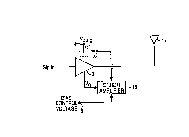
FIG. 4 shows stage 3 of a power amplifier as in FIG.
1. In accordance with the invention, current detector g
detects the current flowing to the drain terminal of the
S stage 3 FET, and provides a signal ~I (indicative of the
drain current) to one input terminal of an error amplifier
16, the other input terminal of which receives the bias
control voltage from terminal 8. Error amplifier 16 then
output~ a control signal (the result of comparing its two
10 input signals) to the gate terminal of stage 3, thereby
controlling the operating point of stage 3.
FIG. 5 shows one embodiment of the present invention
including detail in addition to that of Fig. 4. (Each
stage 1, 2, 3 is identical to the corresponding prior art
15 stages depicted in FIG. 1.) Power supply voltage VDD is
supplied via resistor 11 to the drain terminal of stage 3.
The voltage across resistor 11 is proportional to the
drain current to stage 3. Resistor 11 thus detects the
current flowing to the FET drain terminal of stage 3, and
20 has in one embodiment a resistance value equal to or
smaller than 1 ohm (typically being 0.1 ohm), to minimize
the resulting drop in the voltage supplied to the drain
terminal (i.e., minimize power dissipation in the
detection resistor 11).
Voltages at each end of resistor 11 are supplied via
resistors 12, 13 to respectively the non-inverting and
inverting terminals of op amp (operational amplifier) 14,
which is a typical op amp. Resistors 12, 13, lS and 20
determine the gain of op amp 14. In the general case, if
30 the res~stance Rll of resistor 11 is much less than
resistances R12, R13 of respectively resistors 12, 13:
R2
WO94t~491 PCT/US94/03299
2136749 8 -
where:
VDD = drain supply voltage
VDDapplied = output of Rll, input to stage 3.
In one embodiment, resistance R12 of resistor 12 is
5 equal to the resistance R13 of resistor 13, and the
resistance R20 of resistor 20 is equal to the resistance
R15 of resistor 15, and Vout = -(R15/R13)~, where ~ is
equal to the drop across resistance Rll.
In order to determine the values of R12, R13, R15 and
10 R20, the desired control voltage versus ouL~uL power
versus drain current is determined; this relation varies
between applications. In one example, for a 10-fold gain,
resistor 13 is lOK ohms and resistor 15 is lOOK ohms.
The output signal of op amp 14 is input, together
15 with the externally provided bias control voltage, to
Le~E_Lively the inverting and non-inverting terminals of
op amp (error amplifier) 16. Capacitor 17 is connected
between the inverting terminal and the output terminal of
op amp 16, so that op amp 16 serves an integrator.
Op amp 16 controls the gate voltage, and hence
indirectly the drain current, of stage 3. When the
feedback loop is closed, the output signal of op amp 14,
which is y~o~o~ional to the drain current of stage 3,
will be equal to the control voltage. The values of
25 resistors 12, 13, 15 and 20 are chosen so that the desired
relationship between control voltage and the stage 3 drain
CU~ is achieved.
The ~G..L-ol voltage input to amplifier stage 3 is
related to the desired output RF power from amplifier
30 stage 3. The output signal of op amp 16 is input to the
gate (control) terminal of the FET of amplifier stage 3 as
the control voltage.
In this configuration, the control voltage from
amplifier 16 indirectly controls the current drawn by
35 stage 3 of the amplifier by directly controlling the gate
voltage of stage 3. Since the current versus load curve
W094t~491 ~ 7 Ll 9 PCT/US94/03299
-
_ g _
changes much less over temperature, load variation, and
drain voltage than does the gate voltage versus load
curve, the circuit as shown in FIG. 5 is more stable over
these parameters than the prior art circuit of FIG. 1. A
S compensation circuit for restraining the temperature
dependent variations in the gain of amplifier stage 3 is
thereby provided by a feedbac~ loop including amplifier
stage 3 and op amps 14, 16.
In the following example, it is assumed that the
10 level (amplitude) of Sig In to amplifier stage 1 is fixed
(and therefore the externally provided bias control
reference voltage related to the Sig In level is also
fixed) and that the amplifier stage 3, and op amps 14, 16
configured for temperature compensation are in a closed
lS loop state. "Closed loop state" means that the output of
op amp 16 generates a gate voltage which results in a
drain current that in turn generates an output signal from
op amp 14 which is equal to the desired control voltage.
In other words, the closed loop is working and the ou~u~
20 of op amp 16 is somewhere in the middle of the range, not
"railed" at one end of its range.
When the ambient temperature rises in this closed
loop state, the subsequent variation in the control
circui~ is as follows:
(a) When the ambient temperature rises, the drain
current is reduced, thus a decline in the gain results.
(b) The voltage at the inverting terminal of op amp
14 incr~~C, due to a reduction in the current flowing
through ~ ent detection resistor 11. Therefore, the
30 output voltage of op amp 14 is reduced. At this time,
ba~ance between the two input voltages of op amp 16 is
lost, and op amp 16 begins to integrate the difference in
voltage at its inputs.
(c) The ouL~L signal of op amp 16 (connected to the
35 FET gate of amplifier stage 3) increases, therefore the
FET drain ~ ent increases. The increase in the drain
WO94/~491 PCT/US94/03299
~367~3
-- 10 --
current leads to a rise in the gain because of the absence
of saturation, with a shift of the operating point on the
load line.
(d) Actions the reverse to those of (a), (b) and (c)
5 occur, and the loop settles to a new steady state closed
loop condition.
As a consequence of the above, the gain and the drain
current at an elevated temperature are, as indicated by
curves G2', I~' in FIG. 6, substantially equal to a gain
10 Gl and a drain current IDI at room temperature, so that the
influence of temperature is reduced.
The above description deals with the case where
ambient temperature rises. In the case of a drop in
ambient temperature, compensation is provided by
15 complementary action.
Further, the present invention also overcomes
variations caused by a variety of non-temperature factors
influencing the FET operating point. For instance,
fluctuations in the load and in the power supply voltage
20 lead to the variations in the FET operating point.
According tc the present invention, such gain variations
are compensAted for.
Therefore, according to the present invention, it is
possible to restrain variations in gain with respect to
25 temperature and other fluctuations, while controlling the
efficiency of the power amplifier. Controlling the other
(two) stages of the amplifier is not critical since they
do not draw a~ much current because they do not produce
large RF oul~u~ ~ignal power. The earlier stages can be
30 biased far from saturating at their RF output power,
without sacrificing a significant amount of power.
The above description is illustrative and not
limiting; the circuit and method in accordance with the
invention are applicable to other types of amplifiers
3S using FETs, and also to those using bipolar transistors,
with appropriate modifications apparent to one of ordinary
WO94/23491 ~13 6 7 4 3 PCT/US94/03299
~ -- 1 1 -- :
skill in the art. The invention is also not limited to RF
amplifiers but applies to other types of analog amplifier
such as baseband or AGC amplifiers.