Note : Les descriptions sont présentées dans la langue officielle dans laquelle elles ont été soumises.
~137430 C5 ~ 3~
TITLE OF THE INVENTION
ULTRASONIC DIAGNOSTIC APPARATUS
BACKGROUND OF THE INVENTION
Field of the Invention
This invention relates to an ultrasonic diagnostic apparatus for
producing an image, for ~x~mple, a sectional image, of an ~x~mined
body by emitting a beam of ultrasonic wave thereinto and receiving
related echoes therefrom.
Description of the Prior Art
Typical ultrasonic diagnostic apparatuses emit a beam of
ultrasonic wave into an ~x~mined body, and receive related
ultrasonic echoes therefrom. The received ultrasonic echoes are
converted into corresponding electric echo sign~l.s. A sectional
image of the ex~mined body is generated in response to the electric
echo sign~ls.
To increase the S/N (signal-to-noise) ratio of the image of the
~x~mined body, a filter tuned to the frequency bands of the electric
echo sign~ is provided which removes noise components from the
electric echo sign~l.s. Generally, the frequency band of an electric
2 0 echo signal moves toward a lower side as the electric echo signal
relates to a deeper portion of an ~ox~mined body. Thus, the filter is
generally of the tunable type, being responsive to a tuning control
signal. The pass band of the filter is adjusted in response to the
tlming control signal so as to match the frequency band of a
currently-processed electric echo signal.
The control-signal response characteristic and the frequency
213743~
response characteristic tend to vary from filter to filter.
Accordingly, in each ultrasonic diagnostic apparatus, complicated
adjustment con~ining manual processes is usually required to
compensate for such a characteristic variation regarding a filter.
SUMMARY OF THE INVENTION
It is an object of this invention to provide an improved
ultrasonic diagnostic apparatus.
A first aspect of this invention provides an ultrasonic
diagnostic apparatus comprising means for emitting ultrasonic wave
into an e~amined body; means for generating a first electric echo
signal in response to an echo of the ultrasonic wave; a controllable
filter responsive to a control signal for extracting components of the
first electric echo signal which are in a desired frequency band, and
thereby converting the first electric echo signal into a second
electric echo signal; a logarithmic detection device for subjecting
the second electric echo signal to logarithmic compression and
detection; a signal generator for outputting plural calibration signals
having different frequencies and different amplitudes; input
selection means for connecting the signal generator with an input
2 0 terminal of the filter during a calibration mode of operation; controlmeans for calc~ ting a corrective value from an output signal of the
logarithmic detection device during the calibration mode of
operation, and correcting a logarithmic conversion characteristic
and an offset of the logarithmic detection device and the control
2 5 signal to the filter in response to the calculated corrective value
during reception of echoes of the ultrasonic wave.
- 2137430
A second aspect of this invention provides an ultrasonic
diagnostic apparatus comprising means for emitting ultrasonic wave
into an e~mined body; means for generating a first electric echo
signal in response to an echo of the ultrasonic wave; a controllable
5 filter responsive to a control signal for extracting components of the
first electric echo signal which are in a desired frequency band, and
thereby converting the first electric echo signal into a second
electric echo signal; a logarithmic detection device for subjecting
the second electric echo signal to logarithmic compression and
10 detection; a signal generator for outputting plural calibration signals
having different frequencies and different amplitudes; input
selection means for connecting the signal generator with an input
terminal of the filter during a calibration mode of operation; a filter
control device for controlling a pass band of the filter at a desired
15 pass band; a gain control device for generating a gain control signal;
an adder for adding an output signal of the logarithmic detection
device and the gain control signal; an A/D converter for converting
an output signal of the adder into a corresponding digital signal; a
reference voltage control device for controlling a reference voltage
20 fed to the A/D converter; a memory for storing an output signal of
the A/D converter; and control means for controlling the input
selection means to connect the signal generator with the input
terminal of the filter during the calibration mode of operation,
controlling the signal generator in accordance with a calibration
2 5 sequence, reading out the signal from the memory and calculating
corrective values for control signals outputted from the filter control
2137430
device, the gain control device, and the reference voltage control
device in response to the readout signal, and correcting the control
sign~l.s outputted from the filter control device, the gain control
device, and the reference voltage control device in response to the
corrective values during reception of echoes of the ultrasonic wave.
A third aspect of this invention provides an ultrasonic
diagnostic apparatus comprising a signal processor having a
controllable signal processing characteristic; means for generating
an electric echo signal; means for generating a predetermined
calibration signal; means for applying the calibration signal to the
processor during a first interval; means for generating a corrective
signal in response to an output signal of the processor during the
first interval; means for applying the echo signal to the processor
during a second interval different from the first interval; and means
for controlling the characteristic of the processor in response to the
corrective signal during the second interval.
It is preferable that the processor includes one of a tunable
filter, a logarithmic detector, and an A/D converter.
BRIEF DESCRIPTION OF THE DRAWINGS
2 0 Fig. 1 is a block diagram of a prior-art ultrasonic diagnostic
apparatus.
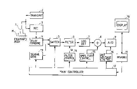
Fig. 2 is a block diagram of an ultrasonic diagnostic apparatus
according to a first embodiment of this invention.
Fig. 3 has a diagram of a relation between a detection value
2 5 and a filter control signal in the apparatus of Fig. l, and also a
diagram of relations between a filter control signal and a filter pass-
2137g3~
band central frequency in the apparatus of Fig. 1.
Fig. 4 is a time-domain diagram of the filter control signal in
the apparatus of Fig. 1.
Fig. 5 is a diagram of a relation between a filter input level and
5 an adder output level in the apparatus of Fig. 1.
Fig. 6 is a block diagram of an ultrasonic diagnostic apparatus
according to a second embodiment of this invention.
DESCRIPTION OF THE PREFERRED EMBODIMENTS
Before the description of embodiments of this invention, a
10 prior-art ultrasonic diagnostic apparatus will be described for a
better understanding of this invention.
With reference to Fig. 1, a prior-art ultrasonic diagnostic
apparatus includes an ultrasonic probe 1 electrically connected to a
transmission circuit 2 and a receiving circuit 3. When the prior-art
1 5 ultrasonic diagnostic apparatus is actually used, the ultrasonic probe
1 rem~ins in contact with the surface of an ex~mined body M such
as a human body.
The ultràsonic probe 1 includes an array of piezoelectric
transducers (electric-ultrasonic transducers). The piezoelectric
2 0 transducers are sequentially activated by electric output signals of
the tr~n~mission circuit 2 so that pulses of a beam- of ultrasonic wave
are emitted into the examined body M.
Echoes of the pulses of the ultrasonic wave bearn are
generated at organs of the ~x~mined body M. The ultrasonic echo
2 5 pulses are received by the ultrasonic probe 1, being converted into
corresponding electric echo sign~l.s thereby. The electric echo
2137430
sign~ls are outputted from the ultrasonic probe 1 to the receiving
circuit 3. The electric echo .sign~ls are in plural ch~nnels.
The electric echo sign~ls are processed by the receiving
circuit 3 into second echo signals. The second echo signals, that is,
5 the output signals of the receiving circuit 3, are applied to a
delaying and combining circuit 4. Regarding each of the (~h~nne
the device 4 provides suitable delay times to the second echo
~sign~ls respectively, and combines the resultant delayed si~n~ls into
a composite echo signal.
Generally, the composite echo signal generated by the
delaying and combining circuit 4 has wide-band noise components
in addition to desired information components. An effective way of
providing a low-noise sectional image of the ~x~mined body M is to
remove noise components from the frequency band of the
15 composite echo signal. Generally, due to characteristics of
ultrasonic wave in a body, an electric echo signal related to a deeper
portion of the body has more attenuated high-frequency
components. Therefore, the frequency band of the composite echo
signal shifts toward a lower side as the composite echo signal
2 0 relates to a deeper portion of the ~x~mined body M.
The composite echo signal is outputted from the delaying and
combining circuit 4 to a tunable filter (a tunable band pass filter) 6.
The tunable filter 6 removes noise components from the composite
echo signal. The tunable filter 6 has a pass band which is shifted in
2 5 response to a tuning control signal fed from a filter control circuit
14. A portion of the examined body M which relates to the current
2137430
composite echo signal moves in depth as time goes by. Thus, the
frequency band of desired information components of the composite
echo signal moves as time goes by. The combination of the tunable
filter 6 and the filter control circuit 14 is designed to compensate
5 for this time-dependent movement of the frequency band of desired
information components of the composite echo signal. Specifically,
the pass band of the tunable filter 6 is shifted so as to follow the
frequency band of desired information components of the composite
echo signal.
1 0 The tunable filter 6 includes a variable capacitance diode. The
pass band of the tunable filter 6 shifts in accordance with a control
voltage applied to the variable capacitance diode. The tuning
control signal outputted from the filter control circuit 14 is applied
to the variable capacitance diode as a control voltage. To shift the
1 5 pass band of the tunable filter 6 with a change in the frequency band
of desired information components of the composite echo signal,
the filter control circuit 14 varies the voltage of the tuning control
signal in a preset curve as time goes by.
A logarithmic detection circuit 7 receives the output signal of
2 0 the tunable filter 6, and reduces the dynamic range of the output
signal of the tunable filter 6 to a level matching the dynamic range
of a display 10. In addition, the logarithmic detection circuit 7
converts the output signal of the tunable filter 6 into a
corresponding intermediate-frequency signal. Specifically, the
2 5 device 7 subjects the output signal of the tunable filter 6 to
logarithmic compression and amplitude envelope detection.
2137~30
A gain control circuit (an amplitude control circuit) 15
outputs a gain control signal to an adder 8. The adder 8 also
receives the output signal of the logarithmic detection circuit 7.
The device 8 adds and combines the output sign~l.s of the
5 logarithmic detection circuit 7 and the gain control circuit 15. The
gain control signal fed from the gain control circuit 15 to the adder
8 is adjusted in response to operator's requirement so that the
brightness of a sectional image on the display lO can be controlled
at a level desired by the operator.
An A/D (analog-to-digital) converter 9 receives the output
signal of the adder 8. The A/D converter 9 changes the output
signal of the adder 8 into a corresponding digital signal while being
controlled in response to reference voltages fed from a suitable
device (not shown). The reference voltages determine the input
15 dynamic range or the input window of the A/D converter 9.
The display lO receives the output signal of the A/D converter
9. The display lO includes a digital sc~nning converter which
changes the output signal of the A/D converter 9 into a
corresponding video signal of a given sc~nning format suited to
20 indication on the screen of the display lO. The display lO indicates
a sectional image of the ~ mined body M on its screen in response
to the output signal of the A/D converter 9.
The tunable filter 6 tends to have the following problem. The
control-signal response characteristic and the frequency response
2 5 characteristic tend to vary from filter to filter. Accordingly, during
manufacture of the prior-art ultrasonic diagnostic apparatus. many
2137430
filter samples are prepared, and one of the samples which has
characteristics near desired characteristics is selected as an
actually-used tunable filter 6. In addition, after the tunable filter 6 is
placed in position within the prior-art ultrasonic diagnostic
5 apparatus, it is necessary to adjust the pass band characteristic of
the tunable filter 6 by human operation. Furthermore, it is
necessary to adjust the logarithmic conversion characteristic (the
logarithmic linearity characteristic) and the offset characteristic of
the logarithmic detection circuit 7 by human operation.
First Embodiment
With reference to Fig. 2, an ultrasonic diagnostic apparatus
according to a first embodiment of this invention includes an
ultrasonic probe 1 electrically connected to the output terminal of a
transmission circuit 2 and the input terminal of a receiving circuit
3. The ultrasonic diagnostic apparatus is also referred to as the
apparatus. The output terminal of the receiving circuit 3 is
connected to the input terminal of a delaying and combining circuit
4. The output terminal of the delaying and combining circuit 4 is
connected to a flrst input terminal of a selector or switch 5.
2 0 The output terminal of a signal generator 13 is connected to a
second input terminal of the switch 5. The signal generator 13 has
a control terminal connected to a main controller 12. The switch 5
has a control terminal connected to the main controller 12. The
output terminal of the switch 5 is connected to the input terminal
2 5 of a tunable filter (a tunable band pass filter) 6. The switch 5 selects
either the output signal of the delaying and combining circuit 4 or
2137430
-1 O-
the output signal of the signal generator 13 in response to a switch
control signal fed from the main controller 12, and transmits the
selected signal to the tunable filter 6.
The tunable filter 6 has a control terminal connected to the
5 output terminal of a filter control circuit 14. The filter control
circuit 14 has a control terminal connected to the main controller
12. The output terminal of the tunable filter 6 is connected to the
input terminal of a logarithmic detection circuit 7. The output
terminal of the logarithmic detection circuit 7 is connected to a
1 0 first input terminal of an adder 8. The output terrninal of an
amplitude control circuit (a gain control circuit) 15 is connected to
a second input terminal of the adder 8. The amplitude control
circuit 15 has a control terminal connected to the main controller
12.
The output terminal of the adder 8 is connected to the input
terminal of an A/D (analog-to-digital) converter 9. The A/D
converter 9 has a control terminal connected to the output terminal
of a reference voltage control circuit 16. The reference voltage
control circuit 16 has a control terminal connected to the main
2 0 controller 12. The output terminal of the A/D converter 9 is
connected to the input terminal of a display 10 and the input
terminal of a memory 11. The output terminal of the memory 11 is
connected to the main controller 12.
Operation of the ultrasonic diagnostic apparatus of Fig. 2 can
2 5 be changed among a first calibration mode, a second calibration
mode, and a normal mode. The first calibration mode of operation
2137430
is designed for adjustment or calibration of the characteristics of
the tunable filter 6. The second calibration mode of operation is
designed for adjustment or calibration of the characteristics of the
logarithmic detection circuit 7. When the ultrasonic diagnostic
5 apparatus is actually used, its operation is set to the normal mode.
Generally, the first calibration mode of operation and the second
calibration mode of operation are executed immediately after the
ultrasonic diagnostic apparatus has been manufactured. Thus, the
first calibration mode of operation and the second calibration mode
10 of operation precede the normal mode of operation.
The main controller 12 includes a microcomputer or a similar
device having a combination of an I/O port, a CPU, a RAM, and a
ROM. The main controller 12 also includes a nonvolatile memory or
a memory supported by a backup system. The main controller 12
15 operates in accordance with a program stored in the ROM. The
program is designed to enable the main controller 12 to execute
various processes which will be described later. Generally, the main
controller 12 selects one of the first calibration mode of operation,
the second calibration mode of operation, and the normal mode of
20 operation in response to a mode selection signal outputted from a
manual switch (not shown).
A description will now be given of the normal mode of
operation of the ultrasonic diagnostic apparatus of Fig. 2. When the
ultrasonic diagnostic apparatus is actually used, the ultrasonic probe
2 5 1 remains in contact with the surface of an ~x~mined body M such
as a human body.
2137430
The ultrasonic probe 1 includes an array of piezoelectric
transducers (electric-ultrasonic transducers). DuAng the normal
mode of operation of the apparatus, the piezoelectric transducers
are sequentially activated by electric output signals of the
transmission circuit 2 so that pulses of a beam of ultrasonic wave are
emitted into the ~x~mined body M.
Echoes of the pulses of the ultrasonic wave beam are
generated at organs of the ex~mined body M. The ultrasonic echo
pulses are received by the ultrasonic probe l, being converted into
corresponding electric echo sign~ls thereby. The electric echo
signals are outputted from the ultrasonic probe 1 to the receiving
circuit 3. The electric echo sign~l.s are in plural ch~nnels.
The electric echo signals are processed by the receiving
circuit 3 into second echo signals. The second echo signals, that is,
the output signals of the receiving circuit 3, are applied to the
delaying and combining circuit 4. Regarding each of the ch~nnels,
the device 4 provides suitable delay times to the second echo
sign~ respectively, and combines the resultant delayed sign~ into
a composite echo signal.
2 0 Generally, the composite echo signal generated by the
delaying and combining circuit 4 has wide-band noise components
in addition to desired information components. An effective way of
providing a low-noise sectional image of the ~x~mined body M is to
remove noise components from the frequency band of the
2 5 composite echo signal. Generally, due to characteristics of
ultrasonic wave in a body, an electric echo signal related to a deeper
21~7430
-1 3-
portion of the body has more attenuated high-frequency
components. Therefore, the frequency band of the composite echo
signal shifts toward a lower side as the composite echo signal
relates to a deeper portion of the ~mined body M.
The composite echo signal is outputted from the delaying and
combining circuit 4 to the switch 5. During the normal mode of
operation of the apparatus, the switch 5 selects the composite echo
signal and transmits the composite echo signal to the tunable filter
6 in response to the switch control signal fed from the main
controller 1 2 .
The tunable filter 6 removes noise components from the
composite echo signal. The tunable filter 6 has a pass band which is
shifted in response to a tuning control signal fed from the filter
control circuit 14. A portion of the examined body M which relates
to the current composite echo signal moves in depth as time goes
by. Thus, the frequency band of desired information components of
the composite echo signal moves as time goes by. The combination
of the tunable filter 6 and the filter control circuit 14 is designed to
compensate for this time-dependent movement of the frequency
band of desired information components of the composite echo
signal. Specifically, the pass band of the tunable filter 6 is shifted so
as to follow the frequency band of desired information components
of the composite echo signal.
The tunable filter 6 includes a variable capacitance diode. The
2 5 pass band of the tunable filter 6 shifts in accordance with a control
voltage applied to the variable capacitance diode. The tuning
2137~3~
-1 4-
eontrol signal outputted from the filter eontrol eireuit 14 is applied
to the variable eapaeitance diode as a eontrol voltage. To shift the
pass band of the tunable filter 6 with a change in the frequency band
of desired information components of the composite echo signal,
5 the filter control circuit 14 varies the voltage of the tuning control
signal in a preset curve as time goes by. The filter control circuit 14
executes the variation of the tuning control signal according to
information of a filter control curve set therein. The filter control
circuit 14 contains a memory for storing the information of the
10 filter control curve.
As will be described later, the operation of the combination of
the tunable filter 6 and the filter control circuit 14 has been
calibrated during the first calibration mode of operation of the
apparatus prior to the normal mode of operation.
The logarithmic detection circuit 7 receives the output signal
of the tunable filter 6, and reduces the dynamic range of the output
signal of the tunable filter 6 to a level matching the dynamic range
of the display 10. In addition, the logarithmic detection circuit 7
converts the output signal of the tunable filter 6 into a
20 corresponding intermediate-frequency signal. Specifically, the
device 7 subjects the output signal of the tunable filter 6 to
logarithmic compression and amplitude envelope detection.
The gain control circuit 15 outputs a gain control signal to the
adder 8. The adder 8 also receives the output signal of the
2 5 logarithmic detection circuit 7. The device 8 adds and combines
the output signals of the logarithmic detection circuit 7 and the gain
2137430
-1 5-
control circuit 15. The gain control signal fed from the gain control
circuit 15 to the adder 8 is adjusted in response to operator's
requirement so that the brightness of a sectional image on the
display 10 can be controlled at a level desired by the operator.
The A/D converter 9 receives the output signal of the adder 8.
The A/D converter 9 changes the output signal of the adder 8 into a
corresponding digital signal while being controlled in response to
reference voltages fed from the reference voltage control circuit 16.
The reference voltages determine the input dynamic range or the
1 0 input window of the A/D converter 9.
The display 10 receives the output signal of the A/D converter
9. The display 10 includes a digital sc~nning converter which
changes the output signal of the A/D converter 9 into a
corresponding video signal of a given scanning format suited to
indication on the screen of the display 10. The display 10 indicates
a sectional image of the ~ mined body M on its screen in response
to the output signal of the A/D converter 9.
A description will now be given of the first calibration mode of
operation of the ultrasonic diagnostic apparatus of Fig. 2. The first
2 0 calibration mode of operation of the apparatus is executed before
the second calibration mode of operation and the normal mode of
operation. The first calibration mode of operation of the apparatus
is designed to adjust or correct (calibrate) information of a filter
control curve set in the fllter control circuit 14.
2 5 During the first calibration mode of operation of the apparatus,
the signal generator 13 outputs a sine-wave (sinusoidal) reference
2137430
-1 6-
signal. The sine-wave reference signal is also referred to as the
calibration signal. The frequency and the amplitude of the output
signal of the signal generator 13 are selected from among
predetermined different frequencies and amplitudes in response to
5 a control signal fed from the main controller 12.
For example, the signal generator 13 is controlled to
sequentially output one of a first reference signal (a first calibration
signal) Sl having a frequency of 2.5 MHz and an amplitude of -9
dBm, and a second reference signal (a second calibration signal) S2
10 having a frequency of 7.0 MHz and an amplitude of-9 dBm.
The output signal of the signal generator 13 is applied to the
switch 5. During the first calibration mode of operation of the
apparatus, the switch 5 selects the output signal of the signal
generator 13 and transmits the selected signal to the tunable filter
15 6 in response to the switch control signal fed from the main
controller 12.
The main controller 12 controls the signal generator 13 so
that the signal generator 13 will output the first reference signal Sl
at a start of the first calibration mode of operation of the apparatus.
20 The first reference signal Sl is transmitted from the signal
generator 13 to the tunable filter 6 via the switch 5. The main
controller 12 controls the filter control circuit 14 so that a filter
control signal (a tuning control signal) VF fed to the tunable filter 6
from the filter control circuit 14 will vary as time goes by. This
2 5 variation in the filter control signal VF sweeps or shifts the central
frequency of the pass band of the tunable filter 6 from a lower side
21374~0
to an upper side.
It is now assumed that the voltage of the filter control signal
VF linearly increases as time goes by, and that the central frequency
of the pass band of the tunable filter 6 linearly varies in accordance
5 with the voltage of the filter control signal VF. During the first
calibration mode of operation of the apparatus, the amplitude
control circuit 15 and the reference voltage control circuit 16 are
controlled by the main controller 12 so that the output signals
thereof will remain at given states suited for calibration.
The first reference signal Sl, that is, the sine-wave
(sinusoidal) reference signal having a frequency of 2.5 MHz and an
amplitude of-9 dBm, is subjected to amplitude modulation due to
the time-dependent variation of the pass band characteristics of the
tunable filter 6. The output signal of the tunable filter 6 is
15 successively processed by the logarithmic detection circuit 7, the
adder 8, and the A/D converter 9. The memory 11 is controlled by
the main controller 12 so that the output signal of the A/D
converter 12 which corresponds to the first reference signal Sl is
stored into the memory 11. As shown in the part (a) of Fig. 3, the
2 0 detection value or level represented by the signal stored in the
memory 11 varies as a function of the voltage of the filter control
signal VF. Specifically, the detection value peaks when the voltage
of the filter control signal VF agrees with a voltage V1. This peak
results from the fact that the level of the output signal of the tunable
2 5 filter 6 is maximized when the central frequency of the pass band of
the tunable filter 6 reaches the frequency (2.5 MHz) of the first
2137430
-1 8-
reference signal Sl. The main controller 12 derives the
correspondence relation between the detection values represented
by the signal stored in the memory 11 and the voltage values of the
filter control signal VF by referring to the control signal fed to the
5 filter control circuit 14. The main controller 12 compares the
detection values with each other to determine the maximum of the
detection values. The main controller 12 detects the voltage value
Vl of the filter control signal VF which corresponds to the
m~ximum of the detection values. The main controller 12 stores
10 information (data) of the voltage value Vl into the internal RAM as a
detection value related to the first reference signal Sl.
Then, the main controller 12 controls the signal generator 13
so that the signal generator 13 will output the second reference
signal S2. The second reference signal S2 is transmitted from the
15 signal generator 13 to the tunable filter 6 via the switch 5. The
tunable filter 6, the logarithmic detection circuit 7, the adder 8, the
A/D converter 9, the memory 11, the main controller 12, the filter
control circuit 14, the amplitude control circuit 15, and the
reference voltage control circuit 16 operate similarly to the
20 previously-described operation on the first reference signal Sl.
Accordingly, the second reference signal S2, that is, the sine-
wave (sinusoidal) reference signal having a frequency of 7.0 MHz and
an amplitude of-9 dBm, is subjected to amplitude modulation due
to the time-dependent variation of the pass band characteristics of
2 5 the tunable filter 6. The output signal of the tunable filter 6 is
successively processed by the logarithmic detection circuit 7, the
21374~0
-1 9-
adder 8, and the A/D converter 9. The memory 11 is controlled by
the main controller 12 so that the output signal of the A/D
converter 12 which corresponds to the second reference signal S2
is stored into the memory 11. As shown in the part (a) of Fig. 3, the
detection value or level represented by the signal stored in the
memory 11 varies as a function of the voltage of the filter control
signal VF. Specifically, the detection value peaks when the voltage
of the filter control signal VF agrees with a voltage V2. This peak
results from the fact that the level of the output signal of the tunable
fllter 6 is m~imi~ed when the central frequency of the pass band of
the tunable filter 6 reaches the frequency (7.0 MHz) of the second
reference signal S2. The main controller 12 derives the
correspondence relation between the detection values represented
by the signal stored in the memory 11 and the voltage values of the
filter control signal VF by referring to the control signal fed to the
filter control circuit 14. The main controller 12 compares the
detection values with each other to determine the maximum of the
detection values. The main controller 12 detects the voltage value
V2 of the filter control signal VF which corresponds to the
m~imum of the detection values. The main controller 12 stores
information (data) of the voltage value V2 into the internal RAM as a
detection value related to the second reference signal S2.
The true relation between the filter control signal and the
filter pass-band central frequency is determined on the basis of the
2 5 detection values Vl and V2 and the frequencies, 2.5 MHz and 7.0
MHz, and is denoted by the straight line in the part (b) of Fig. 3.
2137430
- 2 0 -
The true relation between the filter control signal and the filter
pass-band central frequency is referred to as the detection
characteristics. Also, the relation between the filter control signal
and the filter pass-band central frequency is determined on the
5 basis of design values Vdl and Vd2 and the frequencies, 2.5 MHz
and 7.0 MHz, and is denoted by the broken line in the part (b) of
Fig. 3. This relation between the filter control signal and the filter
pass-band central frequency is referred to as the design
characteristics. Specifically, the filter pass-band central frequency
10 Fdet (MHz) according to the detection characteristics and the filter
pass-band central frequency Fdes (MHz) according to the design
characteristics are given as follows.
Fdet = {4.5/~V2 - Vl)}.VF + {7.0 - 4.5.V2/l~T2 - Vl)~
~--(1)
1 5 Fdes = {4.5/(Vd2 - Vdl)}.VF + {7.0 - 4.5-Vd2/(Vd2 - Vdl)}
~ (2)
As previously described, during the normal mode of operation
of the apparatus, to shift the pass band of the tunable filter 6 with a
change in the frequency band of desired information components of
20 the composite echo signal, the filter control circuit 14 varies the
voltage of the tuning control signal (the filter control signal) by
referring to information of a filter control curve (a variation curve)
preset therein. An example of the initial variation curve or the
design variation curve is denoted by the broken curve in Fig. 4. The
2 5 variable VFint(t) is now introduced to indicate the voltage of the
filter control signal corresponding to the initial variation curve.
2137430
During the first calibration mode of operation of the apparatus,
the main controller 12 generates information of a calibration-
resultant signal and updates the information of the initial variation
curve into the information of the calibration-resultant variation
5 curve. The variable VFcal (t) is now introduced to indicate the
voltage of the filter control signal corresponding to the calibration-
resultant variation curve. Specifically, the main controller 12
calculates the voltage VFcal(t) of the fllter control signal
corresponding to the calibration-resultant variation curve by
10 referring to the following equation.
VFcal(t) = {(V2 - Vl)/(Vd2 - Vdl)~-~VFint(t)
- Vd2 + V2. (Vd2 - Vd 1) / (V2 - Vl ) ~
~ (3)
When the equation (3) is used as a corrective equation for the initial
15 filter control curve (the design filter control curve) set in the filter
control circuit 14, the initial filter control curve VFint(t) denoted by
the broken curve in Fig. 4 is corrected into the calibration-resultant
filter control curve VFcal(t) denoted by the solid curve in Fig. 4.
The main controller 12 replaces the information of the initial
2 0 variation curve with the information of the calibration-resultant
variation curve in the filter control circuit 14. As a result, the first
calibration mode of operation of the apparatus is completed.
A description will now be given of the second calibration
mode of operation of the ultrasonic diagnostic apparatus of Fig. 2.
2 5 The second calibration mode of operation of the apparatus is
executed after the first calibration mode of operation and before the
2~374~0
- 2 2 -
normal mode of operation. The second calibration mode of
operation of the apparatus is designed to adjust or correct the
logarithmic conversion characteristic (the logarithmic linearity
characteristic) and the offset characteristic of the logarithmic
5 detection circuit 7.
Two reference voltages Vt and Vb are preset in the reference
voltage control circuit 16. The reference voltage control circuit 16
serves to adjust the input dynamic range or the input window of the
A/D converter 9 in response to the reference voltages Vt and Vb.
10 The second calibration mode of operation of the apparatus is
executed to generate corrective values for the reference voltages Vt
and Vb. The corrective values enable calibration regarding errors in
the logarithmic conversion characteristic of the logarithmic
detection circuit 7 and offsets generated in the logarithmic
15 detection circuit 7 and the adder 8.
During the second calibration mode of operation of the
apparatus, the signal generator 13 outputs a sine-wave (sinusoidal)
reference signal. The sine-wave reference signal is also referred to
as the calibration signal. The frequency and the amplitude of the
20 output signal of the signal generator 13 are selected from among
predetermined different frequencies and amplitudes in response to
the control signal fed from the main controller 12.
For example, the signal generator 13 is controlled to
sequentially output one of a third reference signal (a third
2 5 calibration signal) S3 having a frequency of 5.0 MHz and an
amplitude of-9 dBm, and a fourth reference signal (a fourth
~37430
- 2 3 -
calibration signal) S4 having a frequency of 5.0 MHz and an
amplitude of-49 dBm.
The output signal of the signal generator 13 is applied to the
switch 5. During the second calibration mode of operation of the
apparatus, the switch 5 selects the output signal of the signal
generator 13 and transmits the selected signal to the tunable filter
6 in response to the switch control signal fed from the main
controller 12.
The main controller 12 controls the signal generator 13 so
that the signal generator 13 will output the third reference signal
S3 at a start of the second calibration mode of operation of the
apparatus. The third reference signal S3, that is, the sine-wave
(sinusoidal) reference signal having a frequency of 5.0 MHz and an
amplitude of-9 dBm, is transmitted from the signal generator 13 to
the tunable filter 6 via the switch 5. The main controller 12
controls the filter control circuit 14 so that the central frequency of
the pass band of the tunable filter 6 will be equal to 5.0 MHz. In
addition, the main controller 12 controls the amplitude control
circuit 15 so that the voltage of the output signal of the amplitude
2 0 control circuit 15 will be equal to O V. Furthermore, the main
controller 12 controls the reference voltage control circuit 16 so
that the reference voltage control circuit 16 will output reference
voltages Vt and Vb m~rimi7.ing the input dynamic range or the input
window of the A/D converter 9.
2 5 The third reference signal S3 is processed by the tunable
filter 6, and the related output signal of the tunable filter 6 is
2137430
- 2 4 -
successively processed by the logarithmic detection circuit 7, the
adder 8, and the A/D converter 9. The memory 11 is controlled by
the main controller 12 so that the output signal of the A/D
converter 12 which corresponds to the third reference signal S3 is
stored into the memory 11. The main controller 12 reads out the
stored signal from the memory 11, and writes the readout signal
into the internal RAM as a detection value V3 related to the third
reference signal S3.
Then, the main controller 12 controls the signal generator 13
so that the signal generator 13 will output the fourth reference
signal S4. The fourth reference signal S4, that is, the sine-wave
(sinusoidal) reference signal having a frequency of 5.0 MHz and an
amplitude of-49 dBm, is transmitted from the signal generator 13
to the tunable filter 6 via the switch 5. The tunable filter 6, the
logarithmic detection circuit 7, the adder 8, the A/D converter 9,
the memory 11, the main controller 12, the filter control circuit
14, the amplitude control circuit 15, and the reference voltage
control circuit 16 operate similarly to the previously-described
operation on the third reference signal S3.
2 0 Accordingly, the fourth reference signal S4 is processed by
the tunable filter 6, and the related output signal of the tunable filter
6 is successively processed by the logarithmic detection circuit 7,
the adder 8, and the A/D converter 9. The memory 11 is controlled
by the main controller 12 so that the output signal of the A/D
converter 12 which corresponds to the fourth reference signal S4 is
stored into the memory 11. The main controller 12 reads out the
21374~0
- 2 5 -
stored signal from the memory l l, and writes the readout signal
into the internal RAM as a detection value V4 related to the fourth
reference signal S4.
The true relation between the filter input level and the adder
output level is determined on the basis of the detection values V3
and V4 and the amplitudes, -9 dBm and -49 dBm, and is denoted
by the straight line in Fig. 5. The true relation between the filter
input level and the adder output level is referred to as the detection
logarithmic conversion characteristics. Also, the relation between
the filter input level and the adder output level is determined on
the basis of design values and the amplitudes, -9 dBm and -49
dBm, and is denoted by the broken line in Fig. 5. This relation
between the filter input level and the adder output level is referred
to as the design logarithmic conversion characteristics. According
to the detection logarithmic conversion characteristics, the level
Vout [volt] of the output signal of the adder 8 is expressed by the
following equation with respect to the level Vin ldbm] of the signal
inputted into the tunable filter 6.
Vout = {(V4 - V3)/40}.Vin + (40-V3 + 9.V4)/49 (4)
The detection logarithmic conversion characteristics given by
the equation (4) agree with the superimposition of the design
logarithmic conversion characteristics and errors caused in the
logarithmic detection circuit 7, and contain offsets generated in the
logarithmic detection circuit 7 and the adder 8. The main
2 5 controller 12 uses the equation (4) as a corrective equation for the
design logarithmic conversion characteristics and the offsets, and
2137~30
- 2 6 -
calculates desired values Vt and Vb of the output reference voltages
from the reference voltage control circuit 16 in response to a
required display dynamic range (an indication dynamic range) of the
apparatus. For ~mple, in the case where the required display
5 dynamic range is equal to 60 dB, the desired value Vt is set equal to
the level of the output signal of the logarithmic detection circuit 7
which corresponds to an input level (amplitude) of 0 dBm while the
desired value Vb is set equal to the level of the output signal of the
logarithmic detection circuit 7 which corresponds to an input level
10 (amplitude) of-60 dBm. Specifically, the main controller 12
calculates the desired values Vt and Vb by referring to the following
equations.
Vt = (40-V3 + 9.V4)/49
Vb = ~tV4 - V3)/40}.(-60) + (40-V3 + 9.V4)/49
1 5 (5)
During the normal mode of operation of the apparatus, the
main controller 12 controls the reference voltage control circuit 16
so that the levels of the reference voltages outputted therefrom will
agree with the desired values Vt and Vb respectively. In the case
2 0 where an amplitude addition "A" [dB] is required with respect to the
output signal of the logarithmic detection circuit 7, the main
controller 12 controls the amplitude control circuit 15 so that the
amplitude control circuit 15 will output a control signal having a
voltage Vamp [V] given as follows.
Vamp = {~V4 - V3)/40}.A (6)
For example, in the case where an amplitude addition of 10 dB is
2'137430
required with respect to the output signal of the logarithmic
detection circuit 7, the voltage Vamp [V] of the output control signal
from the amplitude control circuit 15 is given as follows.
Vamp = {(V4 - V3)/40}- 10
During the second calibration mode of operation of the
apparatus, the main controller 12 stores information of the
detection value V3, information of the detection value V4,
information of the equation (4), and information of the equation (6)
into the nonvolatile memory or the memory supported by the
backup system. As a result, the second calibration mode of
operation of the apparatus is completed.
The ultrasonic diagnostic apparatus of Fig. 2 may be modified
to also use nonlinear components of the relation between the filter
control signal and the central frequency of the pass band of the
tunable filter 6. In this case, it is preferable that the signal
generator 13 is replaced by a signal generator which can produce
additional signals of two or more different frequencies, and that a
corrective equation is derived which includes a third-order
approximate equation.
2 0 The ultrasonic diagnostic apparatus of Fig. 2 may be modified
to also use nonlinear components of the logarithmic conversion
characteristics of the logarithmic detection circuit 7. In this case,
it is preferable that the signal generator 13 is replaced by a signal
generator which can produce additional signals of two or more
different frequencies, and that corrective equations are derived
which include third-order approximate equations.
21~7430
- 2 8 -
Second Embodiment
Fig. 6 shows an ultrasonic diagnosffc apparatus according to a
second embodiment of this invenffon which is similar to the
embodiment of Figs. 2-5 except for design changes indicated
hereinafter.
The ultrasonic diagnosffc apparatus of Fig. 6 includes a linear
detecffon circuit 17 and a selector or switch 18. The input
terminal of the linear detection circuit 17 is connected to the
output terminal of a tunable filter 6. The output terminal of the
linear detecffon circuit 17 is connected to a first input terminal of
the switch 18. The output terminal of a logarithmic detecffon
circuit 7 is connected to a second input terminal of the switch 18.
The output terminal of the switch 18 is connected to a first input
terminal of an adder 8. The switch 18 has a control terminal
connected to a main controller 12. The switch 18 selects either
the output signal of the logarithmic detecffon circuit 7 or the output
signal of the linear detection circuit 17 in response to a switch
control signal fed from the main controller 12, and transmits the
selected signal to the adder 8.
The linear detection circuit 17 serves to subject the output
signal of the tunable filter 6 to only amplitude envelope detection.
On the other hand, the logarithmic detection circuit 7 serves to
subject the output signal of the tunable filter 6 to both logarithmic
compression and amplitude envelope detection.
2 5 During a first calibraffon mode of operaffon of the apparatus,
the switch 18 is controlled by the main controller 12 to select the
21374~0
- 2 9 -
output signal of the linear detection circuit 17. During a second
calibration mode of operation of the apparatus, the switch 18 is
controlled by the main controller 12 to select the output signal of
the logarithmic detection circuit 7.
This embodiment is advantageous in providing a higher
accuracy of calibration related to the tunable filter 6.
Third Embodiment
A third embodiment of this invention is similar to the
embodiment of Figs. 2-5 except for design changes indicated
hereinafter. In the third embodiment. a main controller 12 (see
Fig. 2) responds to a signal generated from an apparatus power
supply switch (not shown). During a start of an ultrasonic diagnostic
apparatus between the moment of movement of the power supply
switch to its on state and the moment of indication of an image on a
display 10 (see Fig. 2), the main controller 12 serves to execute first
and second calibration modes of operation of the apparatus.
Fourth Embodiment
A fourth embodiment of this invention is .simil~r to the
embodiment of Figs. 2-5 except for design changes indicated
2 0 hereinafter. In the fourth embodiment, a manually-operated input
device (not shown) such as a key board is connected to a main
controller 12 (see Fig. 2). A predetermined instruction of starting
first and second calibration modes of operation of an ultrasonic
diagnostic apparatus can be fed to the main controller 12 by
2 5 actuating the input device. This instruction is denoted by a
sequence of characters such as "CAL$ON". When the main
2137~30
- 3 0 -
controller 12 receives this instruction from the input device, the
main controller 12 starts and executes the first and second
calibration modes of operation of the apparatus.
The input device may be used by the operator (the user) for
feeding the apparatus with various instructions such as an
instruction of ch~nging the mode of indication of an image on a
display 10 (see Fig. 2), an instruction of ch~nging the characteristics
of a normal mode of operation of the apparatus, an instruction of
adjusting the characteristics of the indication of the image, and an
instruction denoted by a sequence of characters.
Fifth Embodiment
A fifth embodiment of this invention is similar to the
embodiment of Figs. 2-5 except for design changes indicated
hereinafter. In the fifth embodiment, a main controller 12 (see Fig.
2) is directly connected to a display 10 (see Fig. 2). The display 10
is controlled by the main controller 12 to indicate operating
conditions of an ultrasonic diagnostic apparatus, results of various
measurements, and other information in addition to a sectional
image of an examined body M.
2 0 When first and second calibration modes of operation of the
apparatus are started, the display 10 is controlled by the main
controller 12 to indicate "Calibration Start". During the first
calibration mode of operation of the apparatus for calibration related
to a tunable filter 6 (see Fig. 2), the display 10 is controlled by the
main controller 12 to indicate "Calibration for Filter". During the
second calibration mode of operation of the apparatus for calibration
2137430
- 3 1 -
related to offsets and logarithmic conversion characteristics of a
logarithmic detection circuit 7 (see Fig. 2), the display 10 is
controlled by the main controller 12 to indicate "Calibration for
Log/Det". When the first and second calibration modes of operation
of the apparatus are completed, the display 10 is controlled by the
main controller 12 to indicate "Completed".
It is preferable that, in the main controller 12, predetermined
normal ranges are preset with respect to corrective values for the
characteristics of the tunable filter 6. In this case, the main
controller 12 compares the corrective values with the normal
ranges to determine whether or not the tunable filter 6 is wrong.
When the corrective values exist outside the normal ranges, that is,
when the tunable filter 6 is wrong, the display 10 is controlled by
the main controller 12 to indicate "Calibration Error with Filter". It
is good to execute the indication of the wrong condition of the
tunable filter 6 at an end of the first calibration mode of operation of
the apparatus. In the presence of the wrong condition of the
tunable filter 6, it is preferable to prevent the indication of
"Completed " .
It is preferable that, in the main controller 12, a
predetermined normal range is preset with respect to a difference
of ~T4-V3) in the previously-indicated equation (4) which is
determined by calibration related to the offsets and the logarithmic
conversion characteristics of the logarithmic detection circuit 7. In
this case, the main controller 12 compares the difference of
(V4-V3) with the normal range to determine whether or not the
2137~30
- 3 2 -
logarithmic detection circuit 7 is wrong. When the difference of
tV4-V3) exists outside the normal range, that is, when the
logarithmic detection circuit 7 is wrong, the display 10 is
controlled by the main controller 12 to indicate "Calibration Error
5 with Log/Det". It is good to execute the indication of the wrong
condition of the logarithmic detection circuit 7 at an end of the
second calibration mode of operation of the apparatus. In the
presence of the wrong condition of the logarithmic detection circuit
7, it is preferable to prevent the indication of "Completed".