Note : Les descriptions sont présentées dans la langue officielle dans laquelle elles ont été soumises.
'94~12r~2?~ (h; 22 ; 59 ~ ~ rn~4;~ ~613232~44 ~ ~ V ~~ ~ L P ~ ' ~ ~ T C~ ~ 1
P12
_.__ ~ ~ ~~~~~1~
SEMICONDUCTOR MULTIPLE QUANTUM WELL MACH-ZEHNDER
OPTICAL MODULATOR AND METHOD FOR FABRICATING THE SAME
BACKGROUND OF THE INVENTION
The invention relates to a semiconductor multiple quantum
well Mach-Zehnder optical modulator having a low driving voltage
and a low optical wave guide loss and a method for fabricating
the same.
An optical modulator is expected as one of the most
important elements constituting optical communication systems
and optical information processing systems. In various kinds of.
the optical modulators) a Mach-Zehnder type optical modulator
receives great deals of attention and expectation due to no wave
form deterioration due to a chirping in the modulation light. A
high speed and long distance optical transmission is mainly
limited by the wave form deterioration due to the chirping in
the modulated light. The wave form deterioration due to the
- 1 -
'q~~~?~2?8 (;~1 ?~: a9 ~ ~ 004 1fi13232844G ~ ~ G ~1 I v E R S r. _ r A'E N T
0 C ~ a13
__ ... _ ~- z~3g193
chirping in the modulated light is remarkable as the optical
transmission speed and the optical transmission distance are
large. For those reasons, the Mach-Zehnder type optical
modulator free from any chirping problem is expected as an
optical modulator permitting a high speed and long distance
optical transmission.
When a semiconductor is placed in an electrical field. the
absorption coefficient chap ges with the electrical field. This
phenomenon. has been known as the Franz-Keldysh effect. When a
bulk semiconductor is placed in an electrical field, the
refraction index changes in proportional to the intensity of the
electrical field. When a quantum well or multiple quantum wells
are placed in an electrical field, the refraction index changes
by a quantum conffined Stark effect. The Mach-Zhender type
optical modu7~ator utilizes the phenomenon of the shift of the
refractive index of the wave guide when applied with the
electrical field.
A typical structure of the Mach-Zehnder type optical
modulator comprises two passive regions each of which includes a
Y-branch wave guide and an active region including two of phase
modulation arms on which an electric field is applied. The Mach-
Zehnder type optical modulator having a multiple quantum well
wave guide structure is disclosed in 1993 electron information
and communication conference, C-151, 4-187 reported by Hirohisa
SANG et a1. The multiple quantum well wave guide of the Mach-
Zehnder optical modulator has a ridge wave guide structure. An
- 2 -
-~,1HG~~~~(i~~~~I~nr ~_~~ r~~ i~ rn~rvy~~~ -
incident light wavelength is 1.55 micrometers. The multiple
quantum well structure comprises 30-periods of InGaAs/InAlAs
layers wherein each InGaAs layer serves as a potential well
having a thickness of 6.5 nanometers and each InAlAs layer
serves as a potential barrier having a thickness of 6.0
nanometers so that a band gap wavelength is 1.45 micrometers. A
total length of the Mach-Zehnder type optical modulator is 1.2
millimeters and a length of the active region of the phase
modulation region on which the electrical field is applied is
0.5 millimeters. When the incidental light wavelength is 1.55
micrometers, a half wavelength voltage is 4.2 V and an
extinction ratio is 13 dB as well as an insertion loss is 12 dB.
As described above, the multiple quantum well Mach-Zhender
optical modulator utilizes a change of the refractive index of
the multiple quantum well wave guide by applying an electrical
field on the phase modulation arms in the phase modulation
region. The Mach-Zehnder optical modulator has a smaller size as
compared to a dielectric optical modulator using LiNb03.
In view of further improvements in performances of the Mach-
Zehnder optical modulator, it is very important to further
reduce a driving voltage and a wave guide loss as much as
possible. The Mach-Zhender optical modulator may conduct a phase
modulation of Light confined in the multiple quantum well wave
guide constituting the phase modulation arms by application of
an electrical field thereon. An amount or' the phase shift of the
light depends upon an intensity of the applied electrical field.
- 3 -
s rn ~ nr r lY r nr .n , r ~ r, C
F4sie~~ y ~~1 ~~i : 0;~ °"C v J4_'_' 61~2~~84?u ~ ~ U Ii I ~~ E R s r _
F .. ' R t~~ T ~ 0 1 P1~
239193
The increase of the intensity of the applied electrical field
requires an increase of the driving voltage. The reduction of
the driving voltage of the Mach-Zehnder type optical modulator
requires an improvement in efficiency of the refractive index
change by application of a predetermined electrical field on the
multiple quantum well wave guides in the phase modulation region
of the optical modulator.
It has been known that the refractive index change in
application of the predetermined electrical field o;t the phase
modulation arms of the Mach-Zehnder optical modulator becomes
large as the band gap wavelength of the multiple quantum well
wave guide constituting the phase modulation arms approaches to
the incidental light wavelength. Notwithstanding, if the the
band gap wavelength of the multiple quantum well wave guide
constituting the phase modulation arms approaches to the
incidental light wavelength, then the wave guide loss becomes
large. The large wave guide loss results in a difficulty in
achieving the required long distance optical transmission. The
reduction of the wave guide loss requires a large shift of the
band gap wavelength of the multiple quantum well wave guide from
the incidental light wavelength into a shorter wavelength range.
Consequently. the phase modulation arms in the phase modulation
region on which the electrical field is applied to cause an
optical phase modulation is required to have such an energy band
gap as corresponding nearly to or a bead gap wavelength near to
the incidental light wavelength.
- 4 -
' °4~'='E:?9 (~1 ?3: ~~;~ ~ ~ ~~a4~1fi1~~3~844~ ~~~ I; h~ I Y R R S :.
L F a T F r~ '" v ' F15
X139193
..~...
In the conventional Mach-Zehnder optical modulator, the
multiple quantum well wave guide have the uniform band gap
energy or the band gap wavelength between in the active region
including the phase modulation arms and in the passive regions
including the Y-branches. That is why the conventional Mach-
Zehnder optical modulator having the uniform band gap wavelength
has a problem in difficulty in obtaining botn a iow driving
voltage and a low wave guide loss. If the band gap wavelength of
the multiple quantum well wave guide is largely different from
the incidental light wavelength, then the wave guide loss may be
suppressed but a small refracti~.re index change is obtained by a
larger driving voltage is required to apply the necessary
electrical field on the phase modulation arms for a
predetermined phase shift of the light confined in the wave
guide. By contrast, if the band gap wavelength of the multiple
quantum well wave guide is near to the incidental light
wavelength, then a large refractive index change is obtained
with a Low driving voltage but the wavE guide loss becomes
large.
Therefore. it is required to develop a novel Mach-Zehnder
type optical modulator including a multiple quantum well wave
guide having a difference in the band gap wavelength between the
phase modulation region and the passive region including the Y-
branches.
SUMMARY OF THE INVENTION
- S -
A C
'94~~2~27~ (iii 23: CO ~! ~ CC41i6i323284~iJ ~1~ L T'' I G E R; r. - F ~'I' ..
N T iC 1 FI'?
~~.3g193
Accordingly, it is an object of the present invention to
provide a novel Mach-Zehnder type optical modulator including an
improved multiple quantum well wave guide free from any problem
as described above.
It is a further object of the present invention tc provide a
novel multiple quantum well Mach-Zehnder type optical modulator
showing a large refractive index change with an application of a
small electrical field on a phase modulation region to obtain a
large phase shift of lights.
It is a furthermore object of the present invention to
provide a novel multiple quantum well Mach-Zehnder type optical
modulator being performed with a low driving voltage.
It is a moreover object of the present invention to provide
a novel multiple quantum well Mach-Zhender type optical
modulator having a reduced wave guide loss.
It is another object of the present invention to provide a
novel method of fabricating a Mach-Zehnder type optical
modulator including an improved multiple quantum well wave guide
free from any problem as described above.
It is still another object of the present invention to
provide a novel method of fabricating a multiple quantum well
Mach-Zehnder type optical modulator showing a large refractive
index change with an application of a small electrical field on
a phase modulation region to obtain a large phase shift of
lights.
- 6 -
"~4~'12,q27~ (y) 23 : p l ~ ~ G~ ~--'.11813232&G~0 ~ ~ L' ~' I ~r E R S ~. L F
= '" E N T G ~ 1 18
_ __. .- _
~139I9~
It is yet another object of the present invention to provide
a novel method of fabricating a multiple quantum well Mach-
Zehnder type optical modulator being performed with a low
driving voltage.
It is an additional object of the present invention to
provide a novel method of fabricating a multiple quantum well
Mach-Zhender type optical modulator having a reduced wave guide
loss.
The above and other objects, features and advantages of the
present invention will be described from the following
descriptions.
The invention provides a novel Mach-Zehnder type optical
modulator having multiple quantum well wave guide structure that
comprises two Y-branch portions in passive regions and two phase
modulation arm portions in an active region between the passive
region wherein only the phase modulation arm portions of the
wave guide receives an electrical field. The phase modulation
arm portions of the multiple quantum well wave guide has a band
gap wavelength equal to or near an incidental light wavelength
to cause a large refractive index change by the application of a
low electrical field) while the Y-branch portions of the
multiple quantum well wave guide has a sufficiently small band
gap wavelength than the band gap wave length of the phase
modulation arm portions to thereby suppress a wave guide loss
and reduce a driving voltage of the modulator.
The multiple quantum well wave guide having different band
- 7 _
~1~~~ 9~
gap wavelengths between in the phase modulation arm portions
in the active region and in the Y-branch portions in the
passive regions has a ridge structure that is selectively
grown by use of a metal organic vapor phase epitaxy process
employing silicon oxide mask patterns having a difference in
width between in the active region and in the passive region
and having a uniform gap distance between the mask patterns.
The mask pattern width in the active region is larger than the
mask pattern width in the passive region to grow the multiple
quantum well wave guide in the form of the ridge structure
having in the phase modulation arm portions thereof the band
gap wavelength equal to or near the incidental light
wavelength and in the Y-branch portions the smaller band gap
wavelength.
In accordance with the present invention there is
provided a Mach-Zehnder type optical modulator having a ridge
structure including a multiple quantum well wave guide layer
expending both in a passive region and in an active phase
modulation region on which an electrical field is applied,
wherein said wave guide layer is selectively grown by a metal
organic vapor phase epitaxy with use of dielectric stripe mask
patterns having a large width in said active phase modulation
region and a small width in said passive region so that said
wave guide layer has a band gap wavelength equal to or near a
wavelength of an incidental light in said active phase
modulation region and a smaller band gap wavelength smaller
than said wavelength of said incidental light in said passive
region, said passive region being divided into two regions
_ g _
75983-1
sandwiching said active phase modulation region, and said
ridge structure comprising two Y-branch portions provided on
said divided two passive regions respectively and separated
two phase modulation arm portions on said active phase
modulation region.
In accordance with the present invention there is
further provided a Mach-Zehnder type optical modulator having
two passive regions and an active phase modulation region
sandwiched between said passive regions, said modulator having
a ridge structure including a multiple quantum well wave guide
layer, said ridge structure comprising two Y-branch portions
on said passive regions respectively and two phase modulation
arm portions on said active phase modulation region on which
an electrical field is applied, wherein said wave guide layer
is selectively grown by a metal organic vapor phase epitaxy
with use of dielectric stripe mask patterns having a large
width in said active phase modulation region and a small width
in said passive region so that said wave guide layer has a
band gap wavelength equal to or near a wavelength of an
incidental light in said active phase modulation region and a
smaller band gap wavelength smaller than said wavelength of
said incidental light in said passive regions.
In accordance with the present invention there is
further provided a method of forming a multiple quantum well
wave guide layer having a ridge type structure expending both
on a passive region and an active phase modulation region in a
Mach-Zehnder type optical modulator, wherein said wave guide
layer is selectively grown by a metal organic vapor phase
- 8a -
75983-1
epitaxy with use of dielectric stripe mask patterns having a
large width in said active phase modulation region and a small
width in said passive region so that said wave guide layer has
a band gap wavelength equal to or near a wavelength of an
incidental light in said active phase modulation region and a
smaller band gap wavelength smaller than said wavelength of
said incidental light in said passive region.
BRIEF DESCRIPTION OF THE DRAV~IINGS
Preferred embodiments of the present invention will
hereinafter fully be described in detail with reference to the
accompanying drawings.
FIG. 1 is a perspective view illustrative of a novel
multiple quantum well Mach-Zehnder type optical modulator in a
first embodiment according to the present invention.
FIGS. 2A to 2E are fragmentary cross sectional
elevation views along A-A' line and B-B' line illustrative of
a novel multiple quantum well Mach-Zehnder type optical
modulator in sequential steps involved in a novel method of
fabricating the
- 8b -
75983-1
'94~~2~?7~ L'k) Z3 ; ~Gi ~! ~ G 041_F_323?~440 ~ ~ L1 ~~ I ~~ E R S A ~ F A'~'
E d T iG 1 F~O
~,~ __
2139193
modulator of FIG. i.
FIG. 3 is a view illustrative of a silicon oxide mask
pattewn used in a fabrication step involved in a novel method of
fabricating a novel multiple quantum well Mach-Zehnder type
optical modulator of FIG. 1.
rIG. 4 is a diagram illustrative of a photoluminescence peak
wavelength versus an width of an silicon oxide mask pattern used
in a metal organic vapor phase epitaxy method.
FIG. 5 is a diagram illustrative of acs output light
intensity versus a reverse bias voltage in a novel ~rultiple
quantum well Mach-Zehnder type optical modulator of FIG. 1.
FIG. 6 is a diagram illustrative of an absorption
coefficient and and a refractive index change versus a
wavelength.
FIG. 7 is a perspective view illustrative o' a novel
multiple quantum well Mach-Zehnder type optical modulator in a
second embodiment according to the present invention.
DESCRIPTIOI~IS OF TEiE TIVVEI~ITIOl~1
The invention provides a novel Mach-Zehnder type optical
modulator having multiple quantum well wave guide structure that
comprises two Y-branch portions in passive regions and two phase
modulation arrn portions in an active region between the passive
region wherein only the phase modulation arm portions of the
wave guide receives an electrical field. The phase modulation
_ g _
'94~1~~2?6 l'k~S : n? ~ ~ 0~!L_613e328L40 ~ ~ U E ' v E R S r, L ~ r. ~ E Iu T
~ G v; P?
_ -. ___ ~ 13 919 3
arm portions of the multiple quantum well wave guide has a band
gap wavelength equal to or near an incidental light wavelength
to cause a large refractive index change by the application of a
low electrical field, while the Y-branch portions of the
multiple quantum well wave guide has a sufficient'y small band
gap wavelength than the band gap wave length of the phase
modulation arm portions to thereby suppress a wave guide loss
and reduce.a driving voltage of the modulator.
The multiple wave guide having different band gap
wavelengths between in the phase modulation arm portions in the
active region and in the Y-branch portions in the passive region
has a ridge structure that is selectively grown by use of a
metal organic vapor phase epitaxy process employing silicon
oxide mask patterns having a difference in width between in the
active region and in the passive region and having a un~.form gap
distance between the mask patterns. The mask pattern width in
the active region is larger than the mask pattern width in the
passive region to grow the multiple quantum well wave guide in
the form of the ridge structure having in the phase modulation
arm portions thereof the band gap wavelength equal to or near
the incidental light wavelength and in the Y-branch portions the
smaller band gap wavelength. The variation in width of the
dielectric mask pattern results in variations in composition and
thickness of the wave guide layers grown by use of the
dielectric mask pattern in the metal organic vapor phase epitaxy
process. The variations in composition and thickness of the
- 10 -
'94~12~2 i~ f~' 23: G2 9~ ~ Gu4~? 5_32328446 ~ ~o ~ i V E R S h L ~ ~ ~' E .~
T G G ~ P22
__ ~~39193
multiple quantum well wave guide layers provides variations in
energy band gap and light propagation constant of the multiple
quantum well wave guide. The variations in energy band gap and
light propagation constant of the multiple quantum well wave
guide provides a variation of the band gap wavelength. For those
reasons, the above band gap control technique by use of the
silicon oxide mask pattern having a difference in width between
in the active region and in the passive region may permit only a
single metal organic vapor phase epitaxy process to grow the
ridge structure of the multiple quantum well wave guide having a
difference in the band gap wavelength between in the phase
modulation arm portions and in the Y-branch portions. The phase
modulation arm portions in the active region has the band gap
wavelength equal to or near the predetermined incidental light
wavelength to cause a possible large change in the refractive
index of the arm portions by the application of a low electrical
field on the active region. By contrast, the Y-branch portions
in the passive region has the sufficiently smaller band gap
wavelength than the band gap wavelength of the phase modulation
arm portions in the active region for a possible suppression of
the wave guide loss.
As the band gap wavelength of the multiple quantum well wave
guide is largely different from the incidental light wavelength,
then a low wave guide loss is obtained while a small refractive
index change is obtained even by application of a large
electrical field on the phase modulation arm portions. By
- 11 -
r r n s~ ~ nn ~ r 1
'~4"_~;~~~': ~U) ~~:U: ~r ~~J=li~i32~~84~~~ ~C N I ;l E F, s ~ L F E~'' E N T
C~ v 1 P2
... - ~~,~9193
contrast, as the band gap wavelength of the multiple quantum
well wave guide is equal to or near the incidental light
wavelength, then a large wave guide loss is caused,
notwithstanding, a larger refractive index change of the
multiple quantum well wave guide in the phase modulation region
is obtained by an application of a small electrical field on the
phase modulation region. The larger refractive index change of
the multiple quantum well wave guide with the application of the
small electrical field permits a larger phase shift of the light
confined in the multiple quantum well wave guide in the phase
modulation region on which the electrical field is applied. The
achievement of the required phase shift of the light confined in
the phase modulation arm portions of ~he multiple quantum well
wave guide with the application of the small electrical field
results in a low driving voltage.
From the above descriptions, it could no doubt be
appreciated that the novel structure and fabrication method of
the multiple quantum well wave guide Mach--Zehnder optical
modulator has a low driving voltage and a low wave guide loss
thereby permitting an establishment of a high speed and long
distance optical transmission system.
The following descriptions will focus on preferred
embodiments of the present invention to sufficiently understand
the structure of the novel multiple quantum well Mach-Zehnder
type optical modulator and the novel method far yabric.ating the
modulator.
- 12 -
' 94~y2~2~G (;~;) 2S : U3 ~ r 0 D 1~6' 3~328~~G ~ fi C nT I v E R. S A i. F A
i E ~( T ~~' ~, 1 P24
~13919~
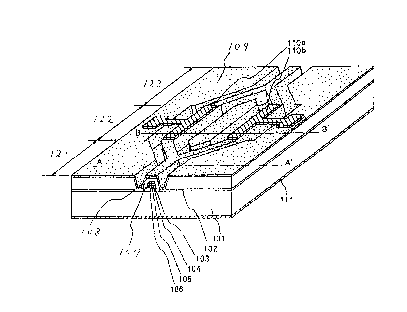
As illustrated in FIG. 1 a novel Mach-Zhender type optical
modulator is formed on an n-InP substrate 101 An n-InP cladding
layer 102 is formed on an entire surface of the top surface of
the substrate 101. The substrate 101 comprises two passive
regions 121 and 123 and an active region 1z2. The ridge
structure is selectively formed to comprise two Y-branch
portions on the passive regions 121 and 123 and two phase
modulation arms on the active region 122. The ridge structure
may comprise multiple layer structure comprising an n-InP buffer
layer 103 on the cladding layer 102, 25 periods of i-
InGaAs/InGaAsP multiple quantum well wave guide layers 104 on
the buffer layer 103, an i-InP cladding layer 105 on the wave
guide layer 104 and p-Ir_P cladding layer 106 on the i-InP
cladding layer 105. A p-InP cladding layer 107 is formed to
cover the layers 102, 103, 104, 105 and 106. A p-InGaAS cap
layer 108 is formed on a top portion of the p-InP cladding layer
107. A silicon oxide film protection layer 109 is formed to
cover an entire surface of the modulator. Two p-side electrodes
110a and IlOb are provided on the cap layer 108 through windows
of the silicon oxide protection layer 109 over the phase
modulation arm portions of the ridge structure in the active
region 122 so as to apply an electrical field on the phase
modulation arm portions. An n-side electrode 111 is provided on
an entire bottom surface of the substrate 101. The above
multiple quantum well wave guide layer 104 of the phase
modulation arm portions has a band gap wavelength that is almost
- 13 -
'~4~;?;~'78 l~k) ?3:0~ ~'iGC~1' 13~3e84w~~~ ~~ U IuT I ~ E R, S ~ L F A'E N T
0 C~ 1 PEE
_ _. __
2139193
the same as or near to the incidental light wavelength, while
the above multiple quantum well wave guide layer 104 of the
phase modulation arm portions has a smaller band gap wavelength
than the incidental light wavelength.
The novel Nach-Zehnder optical modulator may be fabricated
by the following steps. With reference to FIG. 2A, the r.-InP
cladding layer 102 is formed by a metal organic vapor phase
epitaxy on a (i00) face of the n-InP substrate 10i. The cladding
layer 102 has a thickness of 0.3 micrometers and an impurity
concentration of 2 X 10 1~ cm 3. A silicon oxide film is formed
on an entire surface of the n-1nP cladding layer 102 to
subsequently be patterned to form by a photo-lithography a
silicon oxide mask pattern 20I as illustrated in F'IVS. 2B and 3.
The silicon oxide mask pa ten 201 has apertures 202 with a
uniform distance Ww of Z micrometers over both the passive
regions 121 and 123 and the active region 122. The ridge
structure including the multiple quantum well wave guide layer
104 is formed on the aperture 202 cf the mask pattern 201. To
obtain a variation of the band gap wavelength of the multiple
quantum well wave guide layer) the silicon oxide mask patten 201
has difference in width between the passive regions 121 and 123
and the active region 122. Widths Wml and Wm3 of the mask
pattern in the passive regions 121 and 123 is 5 micrometers,
while an width of the mask pattern in the phase modulation
active region 122 is 12 micrometers. The mask pattern 201 has
electrode isolation portions 301 i.n the vicinity of the boundary
- 14 -
° ~4w~~,~L'~'tI~) X3:04 ~!r 9,alifi~323?fiY~ ~~ G.d I GER~~~.: p
~"FJT ~~ C 1 P?fi
_ - ~~,~9193
of the phase modulation active region 122 and the passive
regions 121 and 123 to obtain an isolation between the two p-
side electrodes 110a and 110b. A stripe of the aperture 202 of
the mask is almost directed along a direction (G11) of the
substrate 101.
As illustrated in FIG. 2C, a metal organic vapor phase
epitaxy is carried out by use of the mask pattern 201 to grow
the ridge structure including the multiple quantum well wave
guide layer 104 nn the apertures 2G2 of the mask pattern 201.
The n-InP buffer layer 103, the i-InGaAs/InGaAs multiple quantum
well layer i04, the i-InP cladding layer 105 and the p-InP
cladding layer 106 are sequentiall~° grown by the above metal
organic vapor prase epitaxy method using the mask pattern 202 to
thereby form a mesa structure on the aperture 202 of the mask
pattern 201. The mesa structure has side faces of a (I11)B face.
The n-InP buffer layer 103 has a thickness or 0.1 micrometers.
The i-InP cladding layer 105 has a thickness of 0.1 micrometers.
The p-InP cladding layer lOb has a thickness of 0.2 micrometers
and an impurity concentration of 5 X 101 cm 1. The i-
InGaAs/InGaASP multiple quantum well layer 104 in the active
phase modulation region 122 has 25 periods of inGaAs well layers
latticed matched to the InP layer and InGaAsP potential barrier
layers having a composition wavelength of 1.15 micrometers. In
the phase modulation region 122, the quantum well has a
thickness of 35 angstroms and the potential barrier has a
thickness of 65 angstroms so that in the phase modulation region
- 15 -
' 74~~2,~27~ i~"~) ~3 : G4 ~' ~c 0 u-'_1::6? 523284=~~~ ~ ~ U PI ~ E R S r L F
?~ ~' E Id T G C~ 1 P2
X139193
122 the multiple quantum well wave guide layer 104 has a band
gap wavelength of 1.45 micrometers wherein the incidental light
wavelength is 1.55 micrometers. The total thickness of the
multiple quantum well wave guide layer 104 is 0.25 micrometers.
As described above, the mask pattern 201 has a difference in
width between the passive regions 121 and 123 and the active
phase modulation region 122. The thickness of the quantum well
is proportional to the width of the mask pattern 201. Namely,
increase of she width of the mask patten 201 results in an
increase of the composition. wavelength or the increase of the
band gap wavelength so ti-jat the band gap wavelength of the
multiple quantum well wave guide layer 104 in the active phase
modulation region 122 is larger than the band gap wavelength
thereof in the passive regions 121 and 123. A relationship
between a photo-luminescence peak wavelength of the multiple
quantum well wave guide layer 104 and a mask pattern width is
illustrated in FIG. 4. The mask widths Wml and Wm2 in the active
phase modulation region 122 and the passive regions 121 and 12s
are 12 micrometers and 5 micrometers respectively. The photo-
luminescence peak wavelength is 1.45 micrometers in the active
phase modulation region 122 and 1.41 micrometers in the passive
regions 121 and 123_ From the above descriptions, it could be
understood that the multiple quantum well wave guide layer 104
having the difference in the band gap wavelength or the photo-
luminescence peak wavelength between the active phase modulation
region 122 and the passive regions 121 and 123.
- 16 -
~~~~i2,~? i~ (xi 23: C4 ~~ r~ Ou4_1615?3~8 ~40 ~ ~ G Td I ,' E k S r. ~ P ~ ~
E w T ~~ G 1 P~'S
X139193
With reference back to FIG. 2D. the mask pattern 201 is
selectively removed at opposite side portions with a width of 2
micrometers along the double mesa structure 203 to enlarge the
width of the aperture 202 of the mask pattern 201. A p-InP
cladding layer 107 and a p-TnGaAs cap layer 108 are sequentially
grown on the aperture 202 with the enlarged width of the mask
pattern 201 by the metal organic vapor phase epitaxy. The p-InP
cladding layer 107 and the p-InGaAs cap layer 108 have
thicknesses of 1 micrometer and 0.2 micrometers as well as
impurity concentrations of 5 X 101 cm 3 and 2 X 1018 cm-3
respectively.
with reference to FIG. 2E. a silicon oxide film protection
layer 108 is fo rued on an entire surface of the device. In the
active phase mo3ulation region 122 only, a pair of p-side
electrodes 110a and 110b MADE OF Cr and Au are selectively
formed on the cap layer 108 through windows of the silicon oxide
protection layer 109. The substrate 101 is polished to.have a
thickness of 100 micrometers. Thereafter, the n-side electrode
111 made of Cr and Au is formed on an entire bottom surface of
the substrate 101. Subsequently. the device is cleaved and
receives an anti-reflecting coating on input and output faces
thereof .
The following descriptions will focus on the operations of
the novel Mach-zehnder optical modulator with reference to FIGS.
1. 5 and 6. The incidental light inputted into the Mach-Zehnder
optical modulator is transmitted through the multiple quantum
- 17 -
~4~:;;~2?a(.~)S3:I~ ~!~ 40411c1~2o2S~4.~ ~~ UI4'I~jERSI~ Ffi"'E~IT wjt l ~'9
L:
X13919;
well wave guide layer 104 of the Y-branch portion in the passive
region 121 to be divided into two parts at a ratio of 1:1. The
divided lights in the active phase modulation region 122 are
subsequently transmitted through the phase modulation arm
portions that utilizes the quantum confinement Stark effect. One
of the paired p-side electrodes 110a and 110b is electrically
connected to the n-side electrode 111 being grounded, while
another one of the paired p-side electrodes 110a and 110b
receives a reverse bias. When the reverse bias is OV, then the
light in the phase modulation arm portion receives no phase
shift thereby resulting in no cancellation of the light combined
by the Y-branch portion in the passive region 123. As a result,
an optical output is obtained. In this case, the optical
modulator is placed in ON state. By contrast, the reverse bias
is 3V, then the light in the phase modulation arm portion
receives a phase shift of "pi" thereby resulting in a
cancellation of the lights combined by the Y-branch portion in
the passive region 123. As a result, no optical output is
obtained. In this case, the optical modulator is placed in OFF
state. A relationship of the light output and the reverse bias
voltage is illustrated in FIG. 5.
FIG. 6 illustrates relationships of absorption coefficient
and refractive index change versus the band gap wavelength. In
the active phase modulation region 122, the band gap wavelength
of the wave guide layer 104 is 1.95 micrometers and the
incidental light wavelength is 1.55 micrometers. It could be
- 18 -
rLy : Ly.1 ~v ~L. ~~ ~.~ ~4~~,,~.~., V~~tS~ L TT ~T n ~ ? ' ~!! ~V, F,
p ~ ~ 40 ~~ Utt I a ERar._ Fn. NT ~ , 1 3Q
~139~93
understood that in the active phase modulation region 122 s
light absorption appears but a large refractive index change is
obtained by an application with a small electrical field. This
may permit the driving of the optical modulator is achieved by a
small electrical field on the active phase modulation region
122. This may permit a low voltage driving of the optical
modulator. By contrast, the wave guide layer 104 of the Y-branch
portions in the passive regions 121 and 123 is almost free from
the light absorption or the wave guide loss.
The phase modulation arm portion and the Y-branch portions
are completely and smoothly coupled to each other at almost 100
coupling because the bath portions are grown by the single metal
organic vapor phase epitaxy method according to the present
invention.
The mesa structure by the above method of the novel optical
modulator has a very smooth side face to prevent a scattering
loss of the propagating light in the wave guide.
To reduce a parasitic capacitance of the electrades for a
high speed modulation, polyimide layers 701 are inserted under
pads of the p-side electrodes 110a and 110b as illustrated in
FIG. 7 thereby the optical modulator is available for a high
speed modulation of Gb/s order.
Whereas modifications of the present invention will no doubt
be apparent to a person having ordinary skill in the art, to
which the invention pertains, it is to be understood that
embodiments as shown and described by way of illus~rations are
- 19 -
., -
'94 i2~~7:; ik~ 23 ; cS ~G i~ Cu4ii Ei32S2344v ~ ~ ~ ~' I '~ ~ ~ S r.:: ~ r T
~ r~ i C 0 ' ~ ~1
X139193
by means intended to be considered in a limiting sense.
Accordingly) it is to be intended tc= cover by claims all
modifications of the invention which fall within the sprit and
scope of the invention.
- 20 -
0 I V 1 ' ,