Note : Les descriptions sont présentées dans la langue officielle dans laquelle elles ont été soumises.
-1- 21 ~ 5 7 0 7
Packet Data Receiver With Sampled
Data Output And Background Light Cancellation
Technical Field
This invention relates to digital data receivers and, more particularly, to a
receiver for detecting high-frequency burst-mode packet data superimposed on a
lower
frequency signal.
Background of the Invention
One form of optical communications with increasing commercial importance
utilizes passive sharing of an optical fiber among several optoelectronic
sources and detectors
(hereinafter referred to as "optical busing").
One specific example of optical busing is the "Passive Optical Network" (PON)
illustrated in FIG. 1. Here, several terminal units (Optical Network Units -
ONU) are linked
by one or more passive optical couplers (POC) and optical fibers to a service
provider Optical
Subscriber Unit (OSU) that may in turn be the gateway to an external network.
Data is
transmitted within the network by either or both of time division multiplexing
and wavelength
division multiplexing.
In one currently favoured implementation of a PON, the OSU is allocated a
transmit mode 110 of approximately half of each cycle to transmit information
while the
ONUS "listen" in a receive mode. In the second half of each cycle, the ONUS
are allocated
individual time slots in which to transmit data 120 while the OSU in turn
listens. The data
burst signals transmitted by each ONU during one of these time slots (T1-TN)
are referred to
as a "packet".
Our U.S. Patents 5,025,456, issued on June 18, 1991, 5,371,763, issued on
December 6, 1994, and 5,430,766, issued on July 4, 1995, resolve several
problems faced by
electronic receiver circuits operating in such "burst-mode" packet
communication systems.
Our U.S. Patent '456 describes a fundamental technique for dynamically
establishing a logic threshold voltage centered between the extremes of burst-
mode data
signals, thus solving one well-known problem. The U.S. Patent '763 introduces
a
precision peak detector reset technique for solving the problem of handling
closely spaced
data packets of widely varying amplitude. Our U.S. Patent '766 describes a
technique for
A
X14570'7 -2-
canceling out low-frequency signals due to background light on the optical
bus,
thus solving another problem.
In certain packet communication applications, it may be
advantageous to superimpose on the bus the combination of a low-frequency
signal channel along with the high-frequency packet data. For example, this
low
frequency signal channel might be used for distance ranging or for
communicating audio or terminal status information.
An additional difficulty is that the burst-mode packet data may
have spectral energy in the same frequency band as the low-frequency signal.
Yet, none of these communication channels is permitted to interfere with the
proper detection of any other channel.
Thus, there is a need for a burst-mode packet data receiver which
can properly detect the low-frequency signal channel along with the high-
frequency packet data.
~ummarv of the Invention
In accordance with the present invention, a digital burst-mode
packet data receiver receives high-speed burst-mode packet data signals
combined
with a lower frequency data signal. The receiver includes a first detector for
detecting the received high-speed burst-mode packet data which is reset during
the time period between consecutive bursts of the high-speed packet data
signal.
A second detector samples the lower frequency data signal during a
predetermined portion of the time period between consecutive bursts of the
high-
speed packet data.
More particularly, the present invention solves the prior art
receiver problems by providing:
I. Independent detection of both a high-speed
packet data signal and a low-frequency data signal
which are superimposed on an optical bus at the
same optical wavelength.
II. Low-frequency data detection means which is
insensitive to spectral components of the high-speed
packet data signal that may extend into the
frequency band of the low-frequency data.
III. High-speed packet data signal detection means
which is insensitive to the low-frequency data
21 X5747
-3-
signal and to any other background light on the optical bus.
IV. Low-frequency detection means which does not interfere
with the high-speed packet data path -- by, for example,
imposing special conditions on packet length, packet spacing,
or bit protocol within the packet.
In accordance with one aspect of the present invention there is provided a
digital burst-mode packet data receiver for simultaneously receiving a high-
speed
burst-mode packet data signal and a lower frequency data signal, comprising
first means
for detecting the high-speed burst-mode packet data signal, means for
receiving a reset
signal during a time period between consecutive packet data bursts of the high-
speed
packet data signal, means, responsive to said reset signal, for resetting the
first means for
detecting to a reference, and second means, responsive to said reset signal,
for detecting
the lower frequency data signal during a predetermined portion of the time
period
between consecutive packet data bursts of the high-speed packet data without
interference
from said high-speed burst-mode packet data signal.
In accordance with another aspect of the present invention there is provided
a digital packet data receiver for receiving bursts of digital packet data,
comprising: a
DC-coupled differential input amplifier circuit having first input means for
receiving said
digital packet bursts, second input means for receiving a reference signal,
and output
means for outputting a data output signal; first detector means for detecting
and storing
a peak amplitude of said data output signal and for generating said reference
signal at an
output port; second detector means for generating a sample data output signal
of said data
output signal in response to both an inter-packet reset signal and a sample
control input
signal; and selector means, responsive to said reset signal, for a)
disconnecting said first
detector means output port from said second input means of said input
amplifier circuit
and discharging said peak amplitude signal stored by said first detector
means, and b)
connecting a precision reference voltage as said reference signal to said
second input
means of said input amplifier circuit.
Brief Description of the Drawings
FIG. 1 illustrates an example of optical busing in a Passive Optical Network
(PON) in which the present invention may be utilized.
21 4 57 0 7
-3a-
FIG. 2 shows a block diagram of a packet receiver in accordance with the
present invention.
FIG. 3 shows an illustrative receiver burst-mode packet data signal
superimposed on a low-frequency signal and the signals detected therefrom by
our
receiver.
FIG. 4 shows a table describing the data and reset modes of the present
invention.
FIG. 5 depicts another receiver embodiment for performing packet data and
low-frequency data detection.
Detailed Description
With reference to FIG. 1, there is shown a Passive Optical Network (PON)
in which a receiver, in accordance with the present invention, may be
utilized. In
FIG. 1, each burst-mode data packet in time slots T1-TN would originate,
respectively,
from one of ONU-1 through ONU-N. The burst-mode data packet in time slots Tl
and
T2 are, illustratively, shown in FIG. 3 as each having the same number of data
bits and
different amplitudes P 1 and P2, respectively. These burst-mode data packets
are shown
superimposed on a low-frequency signal 305 which also has to be detected by
the packet
receiver of the present invention.
A packet receiver of the present invention must solve several problems to
be effective in the PON shown in FIG. 1. First, the receiver must dynamically
establish
an effective logic threshold voltage centered between the extremes of the data
signal
swing. Ideally, this data threshold will be substantially established during
the first bit of
an input data burst. Second, because the bus is time-shared by many different
ONU
transmitters which may
2145707 -4-
have widely varying power levels, the receiver electronics must be able to
handle
a wide range of packet amplitudes, separated by only a few bit periods in
time.
Third, because of various causes, there may be background optical signals on
the
bus at much lower frequencies than the data signal. These low-frequency
signals
can prevent proper detection of the high-speed data under certain conditions.
The
receiver must be able to prevent these low-frequency signals from interfering
with proper detection of the data signal.
With reference to FIG. 2, we describe the operation of the present
invention as illustratively implemented in a packet receiver of OSU of FIG. 1.
The packet receiver of the present invention may, illustratively, be used for
reception and resolution of burst-mode data in a packet format having a
predetermined number of bits per packet, as would be used in an Asynchronous
Transfer Mode (ATM) application, for example.
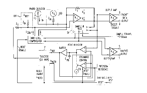
The core of our packet receiver circuit of FIG. 2 includes the
burst-mode receiver architecture of our U.S. patent 5,025,456, consisting of
differential I/O Transimpedance Amplifier A, , Peak Detector PD, and Output
Amplifier A~ .
With reference to FIG. 2, optical input signals representing the
data bits of the burst-mode packet data signal are received and converted by
Photodiode PD1 into Photocurrent Signal I,N. Transimpedance Amplifier A,
converts the currents into a differential output voltage.
The differential output voltage of Amplifier A, is Vo - Vo = I,NZT
where ZT is the transimpedance (feedback resistor) between the positive input
and negative output of A, . One of A, 's differential outputs, and therefore
one
half of the net output swing, is sampled by the Peak Detector and stored on
Capacitor CPD . This half-amplitude reference level, I~"Z~ , establishes the
"instantaneous logic threshold" VReF and is applied to the complementary
(negative) input of A, during normal "data mode" operation. The instantaneous
logic threshold VReF is determined at the beginning of each signal burst. The
logic threshold VREF is set equal to the half-amplitude point of the peak
input
signal, and subsequent signal amplification by A, is referenced to this level.
Threshold VReF determination is very rapid, and ideally is completed by the
conclusion of the first bit in the signal burst.
Variations of signal amplitude from packet to packet are
accommodated using an externally provided RESET input signal to identify the
2145'07
interval between packets, as in our previously referenced patent 5,371,763.
Resetting after receiving each packet data burst ensures that the packet
receiver
can detect a smaller amplitude P2 data packet (e.g., in T2) which immediately
follows a larger amplitude P 1 data packet (e.g., in T 1 ). This RESET input
signal
is an interpacket signal produced by an external circuit that keeps track of
timing
during a received packet and is able to predetermine the end of the packet.
The
RESET input signal causes a Threshold Reset circuit to generate a Reset Enable
signal which causes Reset Discharge circuit to discharge Capacitor CPO using
discharge current lo,s
The Reset Discharge circuit discharges the stored peak amplitude
signal on Capacitor CPO to a non-zero DC voltage , VREFO ~ that is
substantially
equal to the baseline DC voltage stored by the Peak Detector circuit during
the
absence of a received input signal. This DC voltage VREFO is established using
a
Precision Reference circuit. The Reset Discharge circuit may include both
coarse
I S and fine Reset circuits (not shown) which are enabled by the RESET signal.
A
coarse Reset circuit discharges the Detector circuit at a high rate until the
stored
voltage is within a predetermined voltage of the baseline DC voltage, after
which
it is shut off. A fine Reset circuit discharges the Detector circuit at a low
discharge rate until the baseline DC voltage is reached.
The Precision Reference circuit establishes a reference voltage
vREFO whlCh is equivalent to a baseline voltage VREF generated when no input
current I,N is received from Photodetector PD1. The Precision Reference
circuit
is implemented as a "clone" of A, and Peak Detector, except that no
Photodetector PD 1 is used.
The novel capabilities of our packet receiver, shown in FIG. 2,
stem from its incorporation of very high-speed Sampling and Hold circuit SH I
and Selector (analog multiplexer) circuitry S 1.
The Sample and Hold circuit SH 1 may be implemented in a well
known manner. For example, see the article entitled "Fully Bipolar, 120-M
Samples 10-b Track and Hold Circuit," written by Messrs. Vorenkamp and
Verdaasdank and published in IEEE Journal of Solid-State Circuits, Vol. 27,
No.
7, July 1992.
By means of the Sampling and Hold circuit SH1, enabled by a
sample control input signal (320 of FIG. 3) having timing information derived
from the RESET signal, our packet receiver has the capability of detecting the
amplitude of a low-frequency light signal (305 of FIG. 3) component of the
214 5 'T 0 7 -6-
receiver input (300 of FIG. 3) in the brief interval TQ between packets. This
amplitude information is provided at a special low-frequency data or "sampled"
output (340 of FIG. 3). Our packet receiver thus provisionally satisfies the
purpose of requirement I above, by producing both a high-speed packet data
output (330 of FIG. 3) and a low-frequency sampled data output (340 of FIG.
3).
By sampling the received input signal (300 of FIG. 3) during the
"quiet" interval (i.e., 320 occurs during TQ interludes) between packets, we
can
assure that there is no high-speed data signal present. This provisionally
resolves
requirement II above.
After the low-frequency signal has been sampled in the quiet
interval TQ between packets, this value is held by Sample and Hold circuit SH1
and converted to an equivalent differential current (ROMP of FIG. 2) which is
subtracted from the received input signal during the subsequent high-speed
data
packet intervals (e.g., TI, T2 of FIG. 3). Recall that amplifier A, has a
1 S transimpedance of ZT (i.e., 8Vo = I,N =~ ZT ). The background light
compensation
circuit has an equivalent transconductance that is approximately~ZT i.e., the
inverse characteristic of A, . This "dark level compensator" linearly converts
the
voltage stored in SHI to a differential output current, ROMP . according to
this
inverse characteristic. It thus effectively cancels the low-frequency signal
(305 of
FIG. 3) at all times (T1 - TN) as well as any other background light that may
be
present, except for the quiet interval TQ between packets, so that it does not
interfere with burst-mode detection of the high-speed packet data during times
TI
- TN. This resolves requirement III above.
Data packet protocols ensure that there must be a "quiet" interval
TQ between data packets. That is because ( 1 ) there must be a timing cushion
to
prevent adjacent packets (e.g., T1, T2) from interfering with one another, and
(2)
a RESET time is required to discharge the burst-mode Peak Detector, in
preparation for receipt of the next packet. Consequently, sampling during the
quiet interval TQ (using the sample signal) does not violate requirement IV
above
by interfering with the packet data protocols. However, during the RESET input
signal, the output Amplifier A3 should be disabled (by Reset Disable signal)
while the Peak Detector is being discharged. That is necessary because it
would
otherwise have undetermined outputs during the reset operation.
To ensure stable voltage levels within the circuit, we normally
must wait until the end of the Peak Detector RESET operation before we can
X145707 _,_
begin the interpacket sampling operation described above. That requires that
RESET signal and Sampling signal operations be performed sequentially, which
will necessarily increase the required time to complete these operations.
In accordance with the invention, an analog multiplexer (i.e.
Selector S 1 of FIG. 2) is used to isolate the Peak Detector from the input
Amplifier A, during the RESET/Sample operations, so that resetting of the Peak
Detector can proceed simultaneously with low-frequency sampling. This allows a
considerable reduction in the required total time.
The following paragraphs review the operation of our packet
receiver circuit of FIG. 2 during the DATA and RESET modes.
DATA Mode
With reference to the table shown in FIG. 4, during the DATA
mode, the RESET signal is in a negative state. Hence, the Dark Level
Compensator and Output Amplifier A3 are enabled, the Selector S 1 selects the
Peak Detector output uREF , the Discharge circuit is disabled, the Sample and
Hold circuit SH1 is in the hold mode and the sample output is constant.
At the beginning of a data burst, one-half of the peak value of
Amplifier A, 's positive differential output is stored on Peak Detector
Capacitor
CPO , and is routed through the high-speed Selector S 1 (an analog, unity gain
multiplexer) back to the negative input of Amplifier A, . This half-amplitude
signal becomes an effective logic threshold at Amplifier A, 's input, and
subsequent data signals are defined as either logic ONE or ZERO, depending on
whether they are above or below this threshold. The differential signal from
Amplifier A, is then further amplified by output Amplifier A3 and appears
across outputs Q and Q .
RESET Mode
With joint reference to FIGS. 2 and 4, at the conclusion of a data
packet during the quiet interval TQ, a RESET signal is delivered to the packet
receiver. The RESET signal causes several actions to occur: (a) the receiver's
high-speed packet data output Amplifier A3 is disabled, i.e., clamped to a low
(logic ZERO) state (this ensures that that output does not suffer spurious
logic
transitions during RESET); (b) the high-speed Selector S 1 is switched so that
it
provides a fixed DC reference VREFo to the negative input of A, ; (c) the Peak
Detector Capacitor CPO discharge control circuitry is activated; and (d) the
Dark
Level Compensator circuit is disabled or turned off.
214 5 '~ 0 '~ -g-
In the RESET mode, the Peak Detector Capacitor CPO is
discharged to prepare the circuit for the next packet. At about the same time,
a
pulse may be delivered to the Sample and Hold circuit SH 1. This activates the
Sample and Hold circuit SH1, which measures and stores the differential output
of Amplifier A, at this time. Amplifier A, 's output voltage during the
interval
between packets will be related to low-frequency information as well as
background light. This signal is delivered to the Sample Buffer/Amp A4 to
provide an external voltage (sampled outputs S and S ) proportional to the
light
present between packets.
At the conclusion of the RESET signal, the Dark Level
Compensator is again enabled and converts the Sample and Hold signal (from
SH 1 ) into a compensatory differential input current ROMP ~ This compensatory
differential current ROMP exactly cancels the photocurrent due to the low-
frequency signal and also that due to background light.
Note that although the implementation we have described utilizes a
current input, it does not preclude the use of a voltage input (e.g., VS of
190 in
FIG. 2) using well-known techniques in the art for converting current input
Transimpedance Amplifier A, into a voltage amplifier. One example of how this
could be implemented is shown in FIG. 2 using a voltage input source VS and
input impedance Z,N connected to the positive input of Amplifier A, and a
reference voltage VREF~ connected through an input impedance Z,N to the
negative input of Amplifier A, (see 191 ).
Also note that although the detailed implementation we have
described, in FIG. 2, uses an analog Selector S1 in the peak detector feedback
loop to reduce the required packet spacing, as described above, it would be a
straight forward proposition to utilize instead separate amplifier chains (for
the
Sampled output and Packet Data output) along with a voltage input burst-mode
amplifier to accomplish substantially the same purpose, as illustrated in FIG.
5.
There, the Packet Data output is generated via transimpedance
Amplifier Ao , voltage Amplifier A,A , and output Amplifier A3 . The Sampled
output is generated by transimpedance Amplifier Afl , Sample and Hold circuit
SH 1 A and Buffer Amplifier A4A . After the low-frequency signal has been
sampled in the quiet interval TQ between packets, this value is held by Sample
and Hold circuit SH 1 A and converted to an equivalent differential current
(I~OMPI
of FIG. 5) by the "dark level compensator" which is subtracted from the
received
input signal during the subsequent high-speed data packet intervals (e.g., T1,
T2
2~45~07
-9-
of FIG. 3). It thus effectively cancels the low-frequency signal (305 of FIG.
3) at
all times (T 1 - TN) as well as any other background light that may be
present,
except for the quiet interval TQ between packets, so that it does not
interfere with
burst-mode detection of the high-speed packet data during times T 1 - TN. By
subtracting compensation current I~OMPI from the input to Amplifier A,A , we
can
eliminate dark currents from the receiver. Optionally, compensation current
ICOMP2 (shown by dotted lines) can be used to eliminate dark currents at the
input to Amplifier Ao . The implementation and operation of the comparable
circuits of FIG. 5 are essentially the same as the similar circuits described
for
FIG. 2.
In the disclosed embodiment, the analog circuit blocks are actually
either well-known ECL gates, or simple modifications of ECL gates. The ECL
gate consists of a differential pair with current source load, followed by an
emitter follower stage. These circuits, while offering limited gain, are
inherently
very fast. The input Amplifier A, , output Amplifier A3 , Peak Detectors,
Buffer
Amplifier, and Precision Reference may be implemented using circuits which are
described in more detail in our article entitled "DC-1Gb/s Burst-Mode
Compatible Receiver for Optical Bus Applications," by Yusuke Ota, et al.,
Journal of Lightwave Technology, Vol. 10, No. 2, February 1992.
While the disclosed embodiment of the present invention is
implemented used bipolar integrated embodiment circuit technology, it should
be
noted that other circuit technologies could be utilized, including FET.
The circuit can be implemented using, for example, silicon,
gallium arsenide or other appropriate semiconductor materials. Moreover, it is
contemplated that other well-known circuits can be used to implement the
amplifier circuit functions shown in FIGS. 2 and 5 without departing from the
teaching of the present invention.
Although the present invention has been described for use with
optical signals, it should be understood that the present invention can be
utilized
in non-optical signals as well.